

Abstract
In this work, an ultra-fast all-optical plasmon induced transparency based on a metal–insulator–metal nanoplasmonic waveguide with two Kerr nonlinear ring resonators is studied. Two-dimensional simulations utilizing the finite-difference time-domain method are used to show an obvious optical bistability and significant switching mechanisms of the signal light by varying the pump-light intensity. The proposed all-optical switching based on plasmon induced transparency demonstrates femtosecond-scale feedback time (90 fs), meaning ultra-fast switching can be achieved. The presented all-optical switch may have potential significant applications in integrated optical circuits.
Export citation and abstract BibTeX RIS
1. Introduction
The diffraction limit of light is recognized as a prevailing challenge in miniaturization and high-density optical circuit integration. Plasmonic structures have the unique capability to manage and guide light at below the diffraction limit utilizing surface plasmon polariton (SPP) propagation at metal–dielectric interfaces. SPPs are dispersive electromagnetic waves coupled to the electrons of a plasma in a conductor and dielectric interface [1, 2]. Strong confinement of SPPs at metallic interfaces of plasmonic nanoscale devices leads to deep subwavelength optical mode confinement and this leads to the development of different applications of integrated optical devices in nanoplasmonics fields [3]. Recently, numerous structures and devices based on SPPs have been studied and investigated, such as modulators [4], demultiplexers [5, 6], filters [7], interferometers [8], nanosensors [9, 10], and optical switches [11–13]. Subwavelength metal–insulator–metal (MIM) waveguides coupled to cavities have been considered by researchers for a wide range of applications [14–16] due to their advantages of subwavelength mode confinement capability, easy integration, and fabrication. The MIM structures consist of two metallic claddings and a dielectric waveguide, which strongly confine the incident light in the dielectric area. The plasmonic excitation leads to very high electric field intensities which make it possible to utilize a nonlinear effect in plasmonic devices [17].
Lately, researchers have studied bistability utilizing plasmonic nanostructures. Optical bistability or multistability, occuring in a system that has two, or more than two, stable states, is mostly shown by the output intensity of the system as a function of the input intensity. In recent years, various optical bistability and switching methods have been theoretically and experimentally reported in plasmonic waveguide-cavity coupled structures. By using a gain medium within the plasmonic cavity switching mechanism, the optical bistability is accessible by adjusting the absorption coefficient in the plasmonic cavity [18, 19]. Various other plasmonic switches based on cavity-coupled waveguides have been illustrated by modifying the optical characteristics of a nonlinear material by a control beam [11, 20–22].
In this paper, an analytical and numerical study of all-optical switching based on plasmon induced transparency in an MIM waveguide side coupled with ring resonators containing Kerr material is presented. A switching mechanism is described analytically and findings considered by 2D finite-difference time-domain simulations.
2. Device description and analytical model
Figure 1 shows a schematic of an MIM waveguide coupled to ring nanocavities embedded within a metal substrate. The parameters of the structure are as follows: r1 and r2 are the radii of the ring resonators, rf is the filtering ring radius, dwc represents the distance between the rings and the straight waveguide, dwf is the distance between the filtering ring and the straight waveguide, t1 and t2 are the thicknesses of the rings, tf is the thickness of the filtering ring, Wwg is the width of the waveguide, l is the distance between the two rings and lf is the inter-center distance between the filtering ring and the resonator ring with radius r1. The metal used in our work is silver, where the dielectric function of the considered metal is expressed by the Drude model as follows:

where ε∞ = 9.5 is the dielectric constant at infinite angular frequency, ωp = 8.9488 eV is the bulk plasmon frequency, γ = 0.069 09 eV is the damping constant of the electrons, and j is the imaginary unit [23, 24].
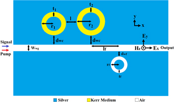
Figure 1. 2D schematic illustration of the proposed plasmonic device.
Download figure:
Standard image High-resolution imageThe nanocavities and the bus waveguide are in dimensions of a subwavelength range so the widths of Wwg ≪ λ. The subwavelength waveguide does not support a transverse electric mode however a transverse magnetic (TM) mode can propagate through the plasmonic waveguide [25–27] The TM SPP mode travels through the waveguide by the propagation constant βwg given by βwg = neff × 2π/λ, where neff is the effective refractive index of the MIM waveguide which can be described as [28, 29]:
Here, εd is the permittivity of dielectric material of the waveguide and εm is the metal permittivity. The Kerr medium permittivity can be written as  where the nonlinear term is dependent on the Kerr medium susceptibility,
  and the average electric field intensity,
  by relation of
The proposed structure switching wavelengths can easily have been manipulated by changing structural parameters. The main structural parameters affecting the resonance wavelength are studied. The structural parameters such as ring size govern the resonance condition and the effects of altering of these on the transmission spectra and resonance wavelengths are shown in figures 2–4. Figure 2 demonstrates the effect of varying ring radii on the transmission response of SPPs. We can obviously see that there are two dips appearing at the transmission spectra, and there is a transparency window between the two dips, with the transparency peak being nearly locating at the center of the two dips. The transmitted dips distance is increased by increasing the difference between the radii of the ring resonators. The other parameters of the structure are set to l = 460 nm, lf = 460 nm, dwc = 10 nm, dwf = 5 nm, rf = 100 nm, t1 = t2 = 40 nm, tf = 40 nm and Wwg = 50 nm. Figure 3 shows the effect of altering thickness on the transmission response of SPPs. The induced transparency profile is blue-shifted by increasing the thicknesses of the ring resonators. The other parameters of the structure are set to l = 460 nm, lf = 460 nm, dwc = 10 nm, dwf = 5 nm, r1 = 127 nm, r2 = 136 nm, rf = 100 nm, tf = 40 nm and Wwg = 50 nm. Notice that in our simulations, the thickness of two ring resonators is equal to each other. The last structural parameter that is investigated here is the distance between the ring resonator and waveguide. Figure 4 demonstrates the effect of varying dwc on the transmission response of SPPs. The induced transparency profile is red-shifted and peak and dips values decrease with a decrease of dwc. The other parameters of the structure are set to l = 460 nm, lf = 460 nm, r1 = 127 nm, r2 = 136 nm, rf = 100 nm, t1 = t2 = 40 nm, tf = 40 nm and Wwg = 50 nm.
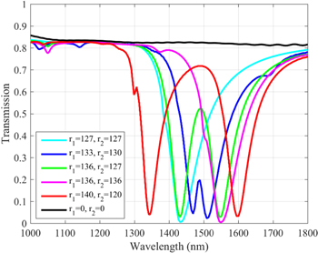
Figure 2. Transmission spectra for different radii of the ring resonators with l = 460 nm, lf = 460 nm, t1 = t2 = 40 nm, rf = 100 nm, tf = 40 nm, dwc = 10 nm, dwf = 5 nm and Wwg = 50 nm.
Download figure:
Standard image High-resolution image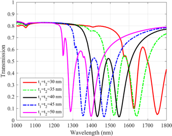
Figure 3. Transmission spectra for different ring resonator thicknesses with l = 460 nm, lf = 460 nm, r1 = 127 nm, r2 = 136 nm, rf = 100 nm, dwc = 10 nm, dwf = 5 nm, tf = 40 nm, and Wwg = 50 nm.
Download figure:
Standard image High-resolution image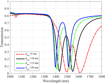
Figure 4. Transmission spectra for different distances between rings and waveguide or dwc with l = 460 nm, lf = 460 nm, r1 = 127 nm, r2 = 136 nm, rf = 100 nm, t1 = t2 = 40 nm, tf = 40 nm, dwf = 5 nm and Wwg = 50 nm.
Download figure:
Standard image High-resolution imageAfter studying the effects of structural parameters on transmission spectra, the parameters are chosen as r1 = 127, r2 = 136, l = 200, t1 = t2 = 40, tf = 40 nm, rf = 100, tf = 40 lf = 400, dwc = 10, and dwf = 50 nm in the following simulations.
When a TM-polarized beam is launched at the structure, the incident light is coupled into the waveguide and the SPPs are propagated at metal interfaces as illustrated in figure 1. At the same time, the incident light is coupled into the nanoring resonators. By satisfying the resonance condition, the traveling wave modes in the nanoring resonator will be excited [30]. It is obvious that the resonant mode depends on the dielectric constant [31, 32] which can be changed by pump light due to the nonlinear medium Kerr effect. Due to the high quality factors of cavities, the resonance field intensity in the cavity will be tremendously enhanced and then lead to a strong nonlinear effect [33, 34]. Near the resonant mode, for two traveling waves, cavities with direct coupling transmission of the waveguide can be expressed by the temporal coupled mode theory (TCMT), described as [34]:
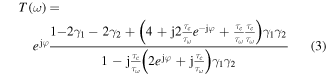
In equation (3) ![${\gamma }_{1}=-1/[2(1/{\tau }_{\omega })({\rm{j}}(\omega -{\omega }_{1})+{\tau }_{i}/2+{\tau }_{\omega }/2)]$](https://content.cld.iop.org/journals/2040-8986/20/5/055504/revision2/joptaab882ieqn5.gif) and
and ![${\gamma }_{2}=-1/[2(1/{\tau }_{\omega })({\rm{j}}(\omega -{\omega }_{2})+{\tau }_{i}/2+{\tau }_{\omega }/2)]$](https://content.cld.iop.org/journals/2040-8986/20/5/055504/revision2/joptaab882ieqn6.gif) where ω stands for the frequency of incident light, ω1 is the resonance frequency of cavity with r1, ω2 is the resonance frequency of cavity with r2, 1/τi represents the decay rate intrinsic loss, 1/τc is the two cavities coupling loss, 1/τω is the waveguide coupling loss and φ is the phase shift induced by the waveguide [34]. At the resonance frequencies ω1 and ω2 the transmission function has dips with minimal values.
where ω stands for the frequency of incident light, ω1 is the resonance frequency of cavity with r1, ω2 is the resonance frequency of cavity with r2, 1/τi represents the decay rate intrinsic loss, 1/τc is the two cavities coupling loss, 1/τω is the waveguide coupling loss and φ is the phase shift induced by the waveguide [34]. At the resonance frequencies ω1 and ω2 the transmission function has dips with minimal values.
3. Results and discussions
In figure 5(a) the blue line shows the transmission spectra of the proposed structure when the pump light is OFF. The dip at 820 nm corresponds to the filtering ring at the right side of the structure.
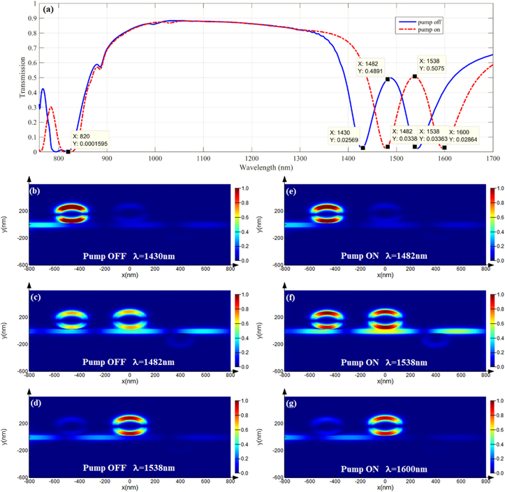
Figure 5. Transmission spectra in the presence of the filtering ring with r1 = 127, r2 = 136, rf = 100, dwc = 10, dwf = 5, l = 200, lf = 400 nm, and t1 = t2 = tf = 40 nm. (a) Blue line is when the pump light is OFF and red line is when the pump light is ON. The intensity of the pump light is 550 MW cm−2. The normalized contour profiles of (Hz) for signal light when the pump light is (b) OFF at λ = 1430 nm, (c) OFF at λ = 1482 nm, (d) OFF at λ = 1538 nm, (e) ON at λ = 1482 nm, (f) ON at λ = 1538 nm, (g) ON at λ = 1600 nm.
Download figure:
Standard image High-resolution imageFigures 5(b)–(d) show Hz distribution when the pump light does not exist. It is observed that the light at λ1 = 1430 nm and λ2 = 1538 nm resonates with the r1 and r2 rings, respectively. As considered from equation (3), figure 5(c) demonstrates a peak between ω1 and ω2 and this is happening at λ = 1482 nm. When the pump light exists, the dielectric constant of the Kerr material is increased by about 0.05 and the red line of figure 5(a) demonstrates that the transmitted dips and peak of the induced transparency profile face to red-shift. The pump light intensity is 550 MW cm−2. Figures 5(e)–(g) show Hz distribution in the presence of the pump light. In the pump light ON condition, the r1 and r2 resonance wavelengths are λ1 = 1482 and λ2 = 1600 nm, respectively. Also the peak of transmission between λ1 and λ1 takes place at λ = 1538 nm. The maximum value for transmission at the 820 nm wavelength is 0.0001 before and after the change of dielectric constant, therefore the pump light is filtered thoroughly. The right side air ring with rf = 100 nm, tf = 40 and dwf = 5 nm filters λ = 820 nm so the air ring causes a dip at λ = 820 nm, therefore it operates as pump light filter. Hence, the pump light cannot reach the output [35, 36]. Accordingly, the wavelength of 820 nm is appropriate for the pump light wavelength and corresponds to the test wavelength of the composite material, Ag-BaO, which is the Kerr nonlinear material chosen in our structure. The third-order nonlinear susceptibility of Ag-BaO at 820 nm is  esu [37, 38]. The transmission values of signal light when the pump light is OFF and ON at λ = 1482 nm and λ = 1538 nm are given in table 1.
Table 1. Transmission values of signal light when the pump light is OFF and ON at λ = 1482 and λ = 1538 nm.
| Description | λ = 1482 nm | λ = 1538 nm |
|---|---|---|
| Transmission of signal light when pump light is OFF | 0.4891 | 0.0336 |
| Transmission of signal light when pump light is ON | 0.0338 | 0.5075 |
Figures 5(c) and (d) show that the designed all-optical switch operates as an enabled-low and enabled-high tri-state switch at λ = 1482 nm and λ = 1538 nm, respectively. On the other hand, when the pump light does not exist the signal light at λ = 1482 nm is allowed to pass the waveguide and at λ = 1538 nm is not allowed to pass the waveguide. Figures 5(e) and (f) demonstrate that in the presence of the pump light, the signal light at λ = 1482 nm is not allowed to pass the waveguide and at λ = 1538 nm it is allowed to pass the waveguide. The transmission of ON state to OFF state T(ON/OFF) at λ = 1482 nm and λ = 1538 nm is 14.47 and 15.03, respectively.
Figure 6 shows the dependence of signal transmission with an increase and decrease of the intensity of the pump light in which an obvious bistability loop can be considered due to the enhanced third-order nonlinear effect of SPPs in the ring resonators that are filled with Kerr material. When the incident pump light intensity increases, the change of the refractive index of the nonlinear material in the ring resonators induced by spatial field intensity gives rise to different transmission effect of signal light. This can provide a mechanism for the bistable behavior of the signal light with the intensity of the pump light [39]. Figure 6(a) shows enabled-low switch at λ = 1482 nm. When the pump light intensity increases, the signal transmission decreases quickly and falls to a lower value at about 300 MW cm−2. However, when the pump light intensity decreases, the signal transmission will sustain lower values until the jumping point of about 250 MW cm−2. The all-optical circuits will be more miniaturized by using this novel type of optical bistability behavior and enabled-low switch. Figure 6(b) demonstrates an enabled-high switch at λ = 1538 nm. When the pump light intensity increases, the signal transmission increases rapidly and rises to a higher value at about 305 MW cm−2. However, when the pump light intensity decreases, the signal transmission will preserve higher values until the dropping point of about 246 MW cm−2. The bistability phenomena will be influenced by the structure geometry, hence a better bistability could be achieved by optimization of the geometrical parameters of the device. In comparison with previous works, the realization of optical bistability only requires a pump intensity of less than 550 MW cm−2 which is less than the results reported in [38].
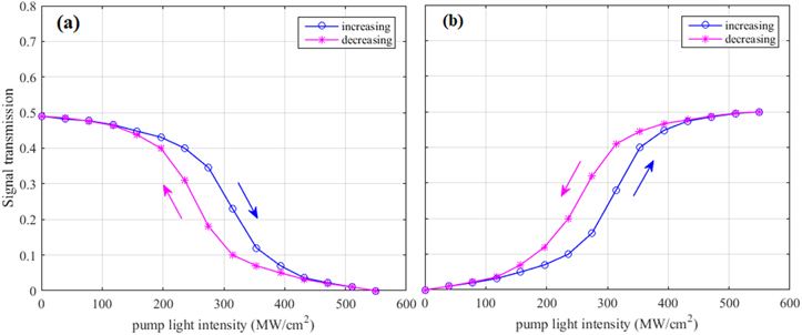
Figure 6. Transmission of signal light by increasing and decreasing the intensity of the pump light with (a) λ = 1482 nm (b) λ = 1538 nm.
Download figure:
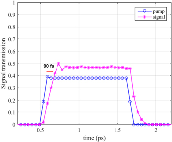
Standard image High-resolution imageFigure 7 demonstrates the time response of the proposed all-optical switch. In order to obtain the time of switching, a square pulse pump light (λ = 820 nm) is launched into the structure with a pulse duration of 1.2 ps and intensity of 550 MW cm−2. It is observed that the response time of the signal light switching up and down is about 90 fs which is remarked as ultra-fast value [39, 40]. Notice that the time of switching is obtained without considering the delay time of the Kerr nonlinear material, therefore it ends with the feedback of the structure [38, 40]. In the structure, the optical Kerr material is the metal–dielectric composite material Ag-BaO with an ultra-fast nonlinear response time of 210 fs [37]. Thus, the results show the femtosecond-level switching in the proposed structure.
Figure 7. The circle line denotes the temporal profile of the pump light with an input intensity of 550 MW cm−2. The starred line corresponds to the signal transmission versus time.
Download figure:
Standard image High-resolution image
4. Conclusions
In this paper, an ultra-fast all-optical plasmon induced transparency plasmonic switch based on a metal–insulator–metal nanoplasmonic waveguide with two Kerr nonlinear ring resonators is introduced and investigated. Two-dimensional simulations utilizing the finite-difference time-domain method are employed in order to show an obvious optical bistability and significant switching mechanisms of the signal light which arise by varying the pump-light intensity. The simulation results show in an enabled-low condition at λ = 1482 nm T(ON/OFF) = 14.45 and in an enabled-high condition at λ = 1538 nm T(ON/OFF) = 15.03, and three different wavelengths can be controlled and switched simultaneously. It is observed that the response time of the switch is about 90 fs, hence this femtosecond-scale feedback time makes possible ultra-fast switching. The proposed all-optical switch may recognize potential significant applications in nanoplasmonic integrated circuits and optical communications.