
Abstract
Lightwave communications is a necessity for the information age. Optical links provide enormous bandwidth, and the optical fiber is the only medium that can meet the modern society's needs for transporting massive amounts of data over long distances. Applications range from global high-capacity networks, which constitute the backbone of the internet, to the massively parallel interconnects that provide data connectivity inside datacenters and supercomputers. Optical communications is a diverse and rapidly changing field, where experts in photonics, communications, electronics, and signal processing work side by side to meet the ever-increasing demands for higher capacity, lower cost, and lower energy consumption, while adapting the system design to novel services and technologies. Due to the interdisciplinary nature of this rich research field, Journal of Optics has invited 16 researchers, each a world-leading expert in their respective subfields, to contribute a section to this invited review article, summarizing their views on state-of-the-art and future developments in optical communications.
Export citation and abstract BibTeX RIS

Original content from this work may be used under the terms of the Creative Commons Attribution 3.0 licence. Any further distribution of this work must maintain attribution to the author(s) and the title of the work, journal citation and DOI.
Table of acronyms
| ADC | analog-to-digital converter |
| ASIC | application-specific integrated circuit |
| AWGN | additive white Gaussian noise |
| CD | chromatic dispersion |
| CMOS | complementary metal-oxide semiconductor |
| DAC | digital-to-analog converter |
| DBP | digital backpropagation |
| DC | datacenter |
| DCF | dispersion compensating fiber |
| DCN | datacenter network |
| DD | direct detection |
| DSF | dispersion-shifted fiber |
| DSP | digital signal processing |
| EDFA | erbium-doped fiber amplifier |
| ENOB | effective number of bits |
| FDM | frequency-division multiplexing |
| FEC | forward error correction |
| FWM | four-wave mixing |
| FMF | few-mode fiber |
| FSO | free space optical |
| HPC | high-performance computing infrastructure |
| IM | intensity modulation |
| LED | light emitting diode |
| MCF | multicore fiber |
| MD | modal dispersion |
| MIMO | multiple-input, multiple-output |
| NFT | nonlinear Fourier transform |
| NLSE | nonlinear Schrödinger equation |
| OFDM | orthogonal frequency-division multiplexing |
| ONU | optical network unit |
| OWC | optical wireless communication |
| PAM | pulse amplitude modulation |
| PDM | polarization-division multiplexing |
| PMD | polarization-mode dispersion |
| PON | passive optical network |
| PSK | phase-shift keying |
| QAM | quadrature amplitude modulation |
| QC | quantum communication |
| QKD | quantum key distribution |
| RF | radio-frequency |
| ROADM | reconfigurable optical add drop multiplexer |
| RS | Reed–Solomon |
| SDM | space-division multiplexing |
| SNR | signal-to-noise ratio |
| SSMF | standard single-mode fiber |
| TDM | time-division multiplexing |
| ToR | top of rack |
| VCSEL | vertical-cavity surface emitting laser |
| VLC | visible light communication |
| WDM | wavelength-division multiplexing |
1. Introduction
Erik Agrell and Magnus Karlsson
Chalmers University of Technology
Today's society relies on fast and reliable exchange of information. Advanced communication systems support the operation of industries, businesses and banks; vehicles and transportation systems; household entertainment electronics and the global flow of news and knowledge. High-quality transmission of real-time video reduces the need for energy-consuming transportation of documents and people, thereby contributing to a sustainable environment. Numerous emerging services and applications, for example, medical diagnosis and treatment, traffic safety and guidance and the Internet of things, are waiting around the corner, stretching the needs for high-capacity communications even further. The long-term trend is illustrated in figure 1, which shows the dramatic growth of global Internet traffic, according to Cisco's statistics and predictions [1].

Figure 1. The past and predicted growth of the total Internet traffic [1].
Download figure:
Standard image High-resolution imageThe information highways that make these services possible consist almost exclusively of optical fibers. No other known medium can support the massive demands for data rate, reliability and energy efficiency. After pioneering experiments in the 1960s and 70s, optical fibers were laid down for commercial deployment in the 1980s and 90s, replacing the older copper wires and communication satellites for long-distance transmission. The race for ever better performance continues and the capacity of a single fiber has been boosted by several orders of magnitude, from a few Gb/s in 1990 to hundreds of Tb/s today, so far more or less keeping up with society's rapidly growing demands.
The tremendous progress in optical communications research is the fruit of the combined efforts of researchers from diverse disciplines. The expertise needed to design a high-performance optical communication system ranges from physics to photonics and electronics, from communication and signal processing algorithms to network technologies. The purpose of this roadmap article is to survey the state-of-the-art in optical communications from multiple viewpoints, and envision where this rapidly evolving field might progress in the future. Due to the broad, interdisciplinary character of the research field, the paper is a joint effort by many researchers, each one being a leading expert in a certain subfield of optical communications. Together we aim to provide a broad overview of optical communications as a whole.
The roadmap article can be coarsely divided in four blocks, covering the optical communications field: hardware, algorithms, networks and emerging technologies. After an initial historical overview, the first block covers the optical hardware needed for high-speed, low-loss lightwave transmission. This block consists of four sections, covering in turn optical fibers, optical amplification, spatial division multiplexing and coherent transceivers. Then follows the block on communication and signal processing algorithms, which describes how to efficiently encode digital data onto lightwaves and to recover the information reliably at the receiver. The five sections in this block cover, respectively, modulation formats, digital signal processing (DSP), optical signal processing, nonlinear channel modeling and mitigation and forward error correction (FEC). The third block lifts the perspective from point-to-point links to networks of many interconnected links, where the three sections cover the technologies needed in different kinds of networks: long-haul, access and data center networks. In the fourth and last block, finally, some emerging technologies are described, which are currently undergoing intense research and may potentially provide disruptively different solutions to future optical communication systems. These technologies are optical integration and silicon photonics, optical wireless communication (OWC) and quantum communication (QC).
Acknowledgments
We wish to sincerely thank all coauthors for their contributions and Jarlath McKenna at IOP Publishing for the coordination in putting this roadmap together.
2. History
A R Chraplyvy
Bell Labs, Nokia
The vision and predictions of Charles Kao and George Hockham in 1966 of ultra-low loss silica glass [2] and the first demonstration of <20–dB/km optical fiber loss in 1970 [3] gave birth to the age of optical fiber communications. In 1977 the first test signals were sent through a field test system in Chicago's Loop District. Within months the first live telephone traffic was transmitted through multimode fibers by GTE (at 6 Mb/s) and AT&T (at 45 Mb/s) and the first era in the age of fiber telecommunications began.
We are currently in the third major era in the age of fiber communications. The first era, the era of direct-detection, regenerated systems began in 1977 and lasted about 16 years. Some of the key milestones of that era follow (a complete early history circa 1983 can be found in a comprehensive review paper by Li [4]). In 1978 the first 'fiber-to-the-home' was demonstrated as part of Japan's Hi OVIS project. The use of multimode fibers and 850 nm wavelengths in trunk systems was short-lived because of ever increasing capacity demands. The first 1300-nm systems debuted in 1981 and the transition to single-mode fibers began with the British Telecom field trial in 1982. The first submarine fiber to carry telephone traffic was installed in 1984. The remainder of the decade witnessed ever increasing commercial bit rates, from 45 Mb/s, to 90, 180, 417, and finally AT&T's FT-G system operating at 1.7 Gb/s. (As an aside, the FT-G system 'anticipated' the wavelength-division-multiplexing (WDM) revolution by implementing two wavelengths around 1550 nm to double the capacity to 3.4 Gb/s.) The synchronous optical network rate of 2.5 Gb/s was first introduced in 1991. Of course, results from research laboratories around the world far exceeded the performance of commercial systems. 2, 4, and 8 Gb/s time-division multiplexing (TDM) rates were demonstrated between 1984 and 1986. The first 10 Gb/s experiments occurred in 1988 and 16 Gb/s and 20 Gb/s systems experiments were demonstrated in 1989 and 1991, respectively. But by that time it was becoming obvious that the days of the first era of optical communications were numbered.
The development of practical erbium-doped fiber amplifiers (EDFA) in the late 1980s [5, 6] (section 4) held out the promise of completely unregenerated long-haul systems and heralded WDM, the next era of optical communications. Unfortunately the existence of optical amplifiers was not sufficient for introduction of large scale WDM at high bit rates. The two existing fiber types in the early 1990s could not support large-channel-count WDM at bit rates above 2.5 Gb/s. Standard single-mode fiber (SSMF, ITU G.652) had large chromatic dispersion (∼17 ps/nm/km) in the 1550 nm wavelength region. Consequently, the reach of 10 Gb/s signals was only 60 km (figure 2). Recall that in 1993 there were no practical broadband dispersion compensators. Dispersion-shifted fiber (DSF, ITU G.653) was developed specifically to eliminate chromatic dispersion issues at 1550 nm. Indeed, DSF can support 10 Gb/s over many thousands of kilometers (figure 2). Because of this, in the early to mid 1990s large-scale deployments of DSF in Japan and by some carriers in North America were undertaken. This proved to be a major mistake for future WDM applications, because DSF is vulnerable to a particularly insidious optical nonlinear effect called four-wave mixing (FWM). FWM mixes neighboring wavelengths and generates new wavelengths that interfere (coherently when channels are spaced equally) with the propagating signals. FWM requires phase matching, in other words low chromatic dispersion, which was the key 'selling feature' of DSF. In amplified systems using DSF, FWM can be a problem even for individual signal powers below 1 mW and can couple wavelengths many nanometers apart. These shortcomings in existing fiber types led to the invention of TrueWave fiber (now generically known as non-zero dispersion shifted fiber [ITU G.655]) at Bell Labs around 1993. This fiber had low enough dispersion to support 10 Gb/s signals over several hundred kilometers (figure 2), which was the required reach for terrestrial systems in those days, but sufficient chromatic dispersion to destroy the phase matching necessary for efficient FWM generation. The immediate obstacle to 10 Gb/s WDM was eliminated. However it was already clear that 40 Gb/s bit rates were on the horizon and even TrueWave fiber would be dispersion limited. Fortunately the researchers realized that two different 'flavors' of TrueWave were possible, one with positive 2 ps/nm/km dispersion and the other with negative 2 ps/nm/km dispersion. This directly led to the invention of dispersion management in 1993 [7] in which fibers of opposite signs of dispersion are concatenated so that locally there was always enough dispersion to suppress FWM but the overall dispersion at the end of the link was near zero. The first demonstration of dispersion management [7] was a primitive interleaving of short SSMF spans with 'negative (dispersion)' non-zero dispersion shifted fiber spans. Shortly thereafter dispersion compensating fiber (DCF, large negative dispersion and, later, also negative dispersion slope) was invented [8] and the concept of dispersion precompensation was demonstrated. Dispersion management proved to be such a powerful technique in systems design that it evolved into a very active field of research. Ever more clever and complex dispersion mapping techniques were introduced (some examples in figure 3 [9]) and dispersion management became an integral part of all high-speed, high-capacity systems. In terrestrial systems the DCF modules are typically housed at amplifier locations but in submarine systems the dispersion management is typically done 'in-line' with a mixture of SSMF and negative NZDSF transmission fibers [10], ironically quite similar to the first crude dispersion map in 1993. Since dispersion management became requisite for all high-speed, high-capacity systems until 2009 we can arguably identify 1993–2009 as the era of dispersion-managed WDM and the second major 16-year era in the age of fiber communications. By the end of this era commercial systems could support over 80 wavelengths each operating at 40 Gb/s. In research laboratories the first 1 Tb/s experiments were demonstrated in 1996 and by the end of the era 25 Tb/s capacity was demonstrated.

Figure 2. Transmission distance versus bit rate for chirp-free sources at 1550 nm for three standard fibers.
Download figure:
Standard image High-resolution image
Figure 3. Various examples of dispersion maps. (a) uniform fiber; (b) singly-periodic map; (c) doubly-periodic map; (d) aperiodic map. Reprinted with permission from [9], copyright 2007 Springer.
Download figure:
Standard image High-resolution imageEven with the most sophisticated dispersion maps enabling very close channel spacing, eventually the EDFAs ran out of optical amplification bandwidth. The only way to increase system capacity was to adopt more advanced modulation formats [11] (section 7). The ability to transmit multiple bits of information for every symbol period allowed increased capacity without the need for increased amplifier bandwidths. The most primitive advanced modulation formats, binary and quadrature phase-shift keying (PSK), could be detected using existing direct-detection technology by differentially encoding and decoding the data (differential PSK and differential quadrature PSK). But for more complex modulation formats as well as for polarization multiplexing (yielding a doubling in capacity) coherent detection is the preferred detection technique. Being forced by spectral efficiency requirements to revive coherent detection work from the 1980s (but now using new digital techniques) actually accrued many systems benefits. The ability to process the electric field with sophisticated digital-signal-processing application-specific integrated circuits (ASICs) rather than merely manipulating the power envelope of a signal precipitated a wide variety of impairment mitigation. In particular arbitrary amounts of chromatic dispersion could be compensated, in principle, in the electronic domain thereby obviating the need for dispersion mapping and consequently signaling the eventual demise of the era of dispersion management.
Concluding remarks
The age of optical fiber communications is comprised of three distinct (technological) eras: the regenerated direct-detection systems era, the dispersion-managed WDM era, and currently the era of coherent WDM communications [12, 13]. Interestingly, the first two eras each lasted about 16 years. Although regeneration and dispersion management will long be part of the communications landscape, the reason the first two eras have identifiable end points is that, in principle (with no consideration for costs), the technology of the subsequent era could completely supplant the previous technology. The former technologies no longer provided unique solutions to existing fiber communications systems need.
Acknowledgments
I thank Bob Tkach and Peter Winzer for valuable input and Jeff Hecht, whose 'A Fiber-Optic Chronology' provided the timeline of the early days of fiber communications.
3. Optical fibers for next generation optical networks
David J Richardson
University of Southampton
Status
Little more than 13 years after Kao and Hockham identified silica as the material of choice for optical fibers [2] single mode optical fibers with losses as low as ∼0.2 dB/km, approaching the minimum theoretical loss of bulk silica, were demonstrated [14]. Soon after the use of SSMF to construct long haul optical networks became firmly established. Despite various detours along the way to develop fibers with different dispersion profiles, (see section 2 for a brief historical overview and discussion of the associated technical motivations), SSMF in conjunction with the EDFA has become the bed-rock on which the global internet has been built.
Significant improvements in SSMF performance have been made over the years including the development of fibers with relatively large effective area (to minimize the optical nonlinearities responsible for constraining fiber capacity), reduced water content and the realization of loss values down below 0.15 dB/km at 1550 nm. In addition, huge advances have been made in developing methods to manufacture such fibers at low cost and in huge volumes (currently at global rates in excess of 200 million kilometers a year). Despite these improvements SSMF designs have not changed substantially for many years, and in reality there remains only limited scope for further performance optimization [15].
Fortunately, until recently, the intrinsic capacity of SSMF has always been far in excess of what has been needed to address traffic demands and there have always been much more cost-effective ways of upgrading link capacity to accommodate growth than trying to develop a fundamentally new fiber platform (e.g. by simply upgrading the terminal equipment to better exploit the available bandwidth). However, laboratory based SSMF transmission experiments are now edging ever closer to fundamental, information theory based capacity limits, estimated at ∼100–200 Tbit/s due to inter-channel nonlinear effects. This fact has sparked concerns of a future 'capacity crunch' [16], where the ability to deliver data at an acceptable level of cost-per-bit to the customer is increasingly outpaced by demand.
Current and future challenges
As a consequence of the fear of a possible capacity crunch, significant global effort has been mobilized in recent years to explore radically new fiber types capable of supporting much higher capacities by defining multiple transmission paths through the same glass strand, thereby better exploiting the spatial dimension. The hope is that the higher information flow per unit area will enable cost/power saving benefits through the improved device integration and interconnectivity opportunities made possible. This approach to realizing better/more cost-effective network capacity scaling is generically referred to as space-division multiplexing (SDM) [17] (see section 5 for a more detailed discussion).
Advances in science and technology to meet challenges
The range of potential technological SDM approaches is ultimately defined by fiber design and a summary of the leading contenders is shown in figure 4 and described below.

Figure 4. Cartoon illustration of the various primary fiber approaches beyond SSMF currently under investigation for use in next generation optical networks. (Adapted from reference [18].)
Download figure:
Standard image High-resolution imageThe first, and arguably most obvious approach to SDM, is to use an array of thin single-core fibers (fiber bundle), possibly in some form of common coating (multi element fiber) to aid rigidity and handling. These approaches offer significant merits in term of practical implementation; however, the scope for associated device integration is somewhat limited.
A second option is to incorporate the cores into the cross-section of a single glass strand—referred to as multicore fiber (MCF). The fundamental challenge here is to increase the number of independent cores in the fiber cross-section, with the core design and spacing chosen to minimize inter-core cross-talk for a suitably bounded range of cable operating conditions and external dimensions. In this instance, each core provides a distinct independent parallel information channel that can be loaded up to close to the theoretical SSMF capacity with advanced modulation format, dense-WDM data channels. Rapid progress has been made and the results seem to indicate that the maximum number of independent cores one can practically envisage using for long-haul transmission lies somewhere in the range 12–32, although for shorter distance applications higher core counts may be possible. It is to be noted that the first SDM experiments at the Petabit/s capacity level were achieved using a 12-core MCF [18], and the first experiment at the Exabit km/s level (over 7326 km) was achieved in a 7-core MCF [19].
A further SDM approach is to try and establish separate distinguishable information channels within a single multimode core that supports a suitably restricted number of modes. Such fibers are referred to as few-mode fibers (FMFs). Early proof-of-principle work focussed on fibers that support two mode groups (LP01 and LP11) which guide 3 distinct spatial modes allowing for modal degeneracy. Due to the strong likelihood of significant mode-coupling in such fibers, further complicated by modal dispersion (MD), it is generally necessary to exploit electronic DSP techniques to unravel and retrieve the otherwise scrambled data—in much the same way as is done to remove the effects of polarization-mode dispersion (PMD) within current digitally-coherent SSMF systems. To minimize the DSP requirements requires fibers with low MD, and/or the development of MD compensation techniques, with excellent progress now made on both fronts. The current challenge is to scale the basic approach to a greater number of modes. Just recently results on 9 LP-mode group fibers have been reported supporting a total of 15 distinct spatial modes, with transmission over 23.8 km successfully achieved [20]. FMF-data transmission over much longer distances has also been reported, with >1000 km transmission already demonstrated for three mode systems [21].
It is worth mentioning that the FMF concept can be extended to the case of MCFs in which the cores are packed more closely together, such that they become coupled (coupled core fibers) [22]. In this case it is possible to excite super-modes of the composite structure which can then be exploited as a practical orthogonal modal basis-set for FMF-data transmission. This approach offers the merit of providing increased flexibility in terms of engineering the MD and also provides certain advantages when it comes to multiplexing/demultiplexing signals into the individual spatial channels.
So far we have described the basic approaches to SDM as independent, however the most recent research is looking to combine multiple approaches to achieve much higher levels of spatial channel count. In particular combining the FMF and MCF approaches with N modes and M cores respectively, it is possible to realize few-mode MCFs (FM-MCFs) supporting a total of M × N spatial channels. For example, just recently data transmission with a record spectral efficiency of 345 bit/s/Hz was reported through a 9.8 km FM-MCF containing 19 cores, with each core supporting 6 modes, providing a total of 19 × 6 = 114 distinguishable spatial channels [23]. Longer distance data transmission in FM-MCFs has also been reported—the best result to date being 20 WDM channel 40 Gbit/s polarization-division multiplexing (PDM)-quadrature PSK transmission over 527 km of FM-MCF supporting 12 cores, each guiding 3 modes (i.e. 36 SDM channels) [24].
In all of the fibers previously discussed the signals have been confined and propagate within a glass core through the principle of total internal reflection. However, in more recent years the possibility of transmitting light in an air-core within hollow core fibers has been demonstrated. These fibers guide light based on either photonic band gap or anti-resonance effects [25]. This offers the prospect of fibers with ultralow nonlinearity (<0.1% that of SSMF) and potentially ultimately lower losses than SSMF (<0.1 dB/km). Such fibers can in principle be operated in either the single mode or multimode regimes, and provide intriguing opportunities for the development of ultrahigh capacity, ultralow latency networks. The challenges in turning hollow core fibers into a mainstream technology are however onerous, not least from a manufacturing perspective given the complex microstructure (with feature sizes of a few 10's of nm extending over 100 km length scales) and the fact that the minimum loss window lies at longer wavelengths around 2000 nm. This results from the intrinsically different nature of the dominant loss mechanisms at shorter wavelength in these fibers (surface scattering at the hollow core air:glass interface rather than bulk Rayleigh scattering as in SSMF).
Concluding remarks
SSMF has reached a very high level of maturity and as such it is hard to envisage significant further improvement in performance, or indeed that it will ever be easily displaced as the fiber of choice in future optical networks. Nevertheless, an array of potential new fiber types, some more speculative and ambitious than others, are currently being explored in terms of technical feasibility and potential to offer substantial performance and/or cost reduction benefits. Each presents its own technological challenges (including amplification, channel Mux/Demux, DSP etc) that will need to be overcome in a practical and cost effective manner if any of them are ever to become a commercial reality.
4. Amplification and regeneration
Peter M Krummrich
Technische Universität Dortmund
Status
Optical amplifiers are a key element of long haul optical transmission systems [26] and have contributed to the success of optical data transport together with low loss transmission fibers (section 3), compact laser diodes, and high speed photo diodes. The capability to leverage WDM for transmitting multiple channels in a single fiber over distances of several thousand kilometers has enabled a much faster capacity growth than the increase of the channel bitrate achievable by enhancing optoelectronic components. However, this success would not have been possible without the reduction of the cost as well as the energy per transported bit which could be realized together with the capacity increase.
The EDFA is the most widely deployed optical amplifier type due to its excellent compatibility with transmission fibers, energy efficiency and low cost [27]. It provides low noise amplification in a wavelength band from approximately 1530 to 1565 nm with a total bandwidth around 35 nm, the so-called C-band. Another amplifier type, distributed Raman amplification, is used very successfully in laboratory hero experiments to increase capacity or reach [28], but its deployment in commercial systems in the field is by far outnumbered by EDFA only systems.
Phase sensitive parametric amplifiers potentially provide lower noise lumped amplification than phase insensitive EDFAs and even signal shape regeneration (2R) capabilities [29], but they cannot easily replace EDFAs in WDM applications. In order to leverage their advantages, several challenges with chromatic dispersion (CD) and PMD management for the alignment of pump and signal phases as well as handling of high signal powers and halved spectral efficiency had to be solved.
Due to the high cost and power consumption of optoelectronic regenerators, these network elements are only used in large scale continental networks, if a limited number of traffic demands require transmission lengths which exceed the maximum transparent reach of individual channels.
In recent years, capacity increase of new system generations has no longer been realized by increasing the maximum number of WDM channels, but by using the bandwidth of channels in the C-band more efficiently. Coherent detection combined with DSP has facilitated the realization of higher order modulation formats and PDM (sections 6 and 7). These technologies have helped to enhance the spectral efficiency by increasing the number of transported bits per symbol.
Current and future challenges
Optical amplifier research is facing two major challenges: capacity increase and dynamic network operation. The data traffic has grown exponentially in the past and foreseeable increased usage of data transport in combination with new types of applications will most likely stimulate an interest in more capacity (see figure 1). However, installation of new systems can only be justified from an economical perspective, if new solutions provide not only more capacity, but also reduced cost per bit and increased energy efficiency.
In addition, the level of flexibility and dynamic adaptability has to be increased. Since their first deployment in the late 1970s, optical core networks are operated in a rather static mode. After installation of a transponder pair, the channel is usually operating on a given wavelength for many years without being touched. The available capacity is neither adapted to traffic variations during the course of the day nor the seasonal ones, resulting in a waste of energy in periods with lower traffic.
In order to leverage the full potential of software defined networking, the option of flexible rerouting of wavelength channels has to be provided in WDM networks. EDFAs are usually operated in saturation in order to realize decent energy efficiency. Hence, a change in the number of active channels results in power transients of surviving channels. The widely deployed electronic gain control alone is not sufficient to provide full flexibility of wavelength channel rerouting in dynamic networks, as EDFAs are not the only source of power transients [30].
Advances in science and technology to meet challenges
From an amplifier perspective, an increase of the capacity per fiber can be supported by several different approaches. The first one is the least disruptive and enables an extension of the current path of enhancing spectral efficiency. Higher order modulation formats need higher optical SNRs for the increase of the number of bits per symbol.
Hybrid amplification approaches, i.e. a combination of EDFAs with distributed Raman amplification, can help to avoid unacceptable short span lengths or reaches with the new more spectrally efficient modulation formats. Technologies such as bidirectional pumping or higher order Raman pumping, which are already deployed successfully in unrepeatered submarine links, can also be applied to terrestrial links. However, many practical issues, such as laser safety or power handling capabilities of optical connectors have to be solved together with the need for cost and energy efficient pump sources.
Phase sensitive parametric amplifiers also provide potential to lower the optical SNR at the output of a link. However, challenges with reduced spectral efficiency due to the need to transmit the idler and the control of the pump and signal phases at the amplifier input indicate that replacing EDFAs in WDM networks may not be the most attractive application of this amplifier type.
The capacity increase potential of commercial systems for core networks realizable by enhancing spectral efficiency is restricted to a factor of approximately four by the so-called nonlinear Shannon limit (when assuming 2 bit/symbol for current systems, see discussions in section 10). Further capacity increase can be realized by additional wavelength bands. Systems for the L-band, the wavelength region from approximately 1575 to 1610 nm, based on EDFAs are commercially available.
Amplifiers for additional wavelength bands around the spectral loss minimum of silica fibers are realizable by using active fibers doped with other rare earth elements than erbium, for example thulium. These amplifiers support a split band approach—each individual amplifier provides gain in a wavelength band with a width of approximately 35 nm. This approach provides flexibility and options for capacity upgrade on demand, but the operation of several amplifiers in parallel may not result in the most cost and energy efficient solution.
For systems with more than 200 channels or a used bandwidth of more than 70 nm, continuous band amplifiers potentially enable the realization of more efficient solutions. Such amplifiers could be based on lumped Raman amplification, other dopants such as bismuth or quantum dots in semiconductor amplifiers.
The attractivity of other wavelength bands than the C-band could also be increased by the availability of new fiber types with lower loss coefficients than silica fiber (section 3). The spectral loss minimum of these fibers will most likely be located around 2000 nm. Rare earth doped amplifiers suitable for this wavelength region have already been demonstrated [31].
Capacity increase by additional wavelength bands in silica fiber is limited to a factor of approximately five compared to C-band systems. The increasing fiber loss at wavelengths further away from the spectral loss minimum limits the reach. Space division multiplexing offers another approach for capacity increase with a potential for capacities per fiber beyond 1 Pbps in the C-band (section 5). Approaches based on multiple cores in a single cladding, multiple modes in a single core, and a combination of both have been demonstrated. From an amplifier perspective, a single multi mode core provides the most energy efficient solution due to the highest spatial density of channels [32].
In recent years, considerable research effort has been spent to equalize the gain of signals propagating in different modes of a multi-mode fiber. An analogy can be found in the early years of research on EDFAs for WDM operation, where efforts were focusing on a reduction of gain differences of channels at different wavelengths in the active fiber, for example, by using different glass compositions. These activities were stopped rather fast after the demonstration of efficient spectral gain flattening by passive filters. Inspired by this observation, the author proposes to shift the focus of multi-mode amplifier research towards spatial gain flattening by passive filters and low noise amplification of each mode. However, the major challenge should be seen in the realization of amplifiers which enable capacity increase together with a reduction of the cost and energy per transported bit.
An efficient implementation of software defined networking in transcontinental networks will require flexible OEO regeneration. Transponders with variable modulation formats may provide sufficient reach even for the longest paths, but not necessarily at the desired spectral efficiency. Approaches such as regenerator pools [33] can increase flexibility and help to find a better compromise between reach, spectral efficiency and power consumption.
Research on avoiding power transients in optically amplified networks has slowed down significantly in recent years. This should not be interpreted in a way that all relevant questions have been answered. Available solutions are somehow sufficient for the currently used rather static operation of networks. Software defined networking has a large potential to change this situation by stimulating a need for the flexible rerouting of wavelength channels. Strategies to cope with power transients should be revisited and further research on transient suppression is highly desirable.
Concluding remarks
Optical amplifier research has led to very powerful and efficient solutions for current high capacity long haul networks. Research efforts seem to have slowed down due to the availability of sophisticated products. However, the challenges resulting from the predicted ongoing growth of capacity demand and increased network flexibility requirements should motivate the research community to re-intensify efforts. Advances in optical amplifier research can have a very beneficial impact on data transport cost and energy efficiency.
Acknowledgments
The author would like to thank the optical amplifier research community for inspiring discussions during several conferences.
5. Spatial multiplexing
Peter Winzer
Bell Labs, Nokia
Status
Over the past decades, network traffic has been growing consistently between 30% and 90% per year, the exact growth rates varying among traffic types and application areas, transmission distances, and operator specificities [34]. While packet router capacities, rooted in Moore's Law, have been matching the above traffic growth numbers for decades, high-speed optical interface rates have only exhibited a 20% annual growth rate, and the capacities of fiber-optic WDM transmission systems have slowed down from 100% of annual growth in the 1990s to a mere 20% per year (see table 1). The disparity between supply and demand of communication rates in core networks has become known as the optical networks capacity crunch [16].
Table 1. Compound annual growth rates (CAGRs) of communication technologies within the given trend periods.
| Technology scaling | Trend period | CAGR |
|---|---|---|
| Supercomputers | 1995–2015 | 85% |
| Microprocessors | 1980–2015 | 40%–70% |
| Router capacity | 1985–2015 | 45% |
| Router interfaces | 1980–2005 | 70% |
| 2005–2015 | 20% | |
| Transport interfaces | 1985–2015 | 20% |
| Per-fiber WDM capacity | 1995–2000 | 100% |
| 2000–2015 | 20% | |
| Fixed access interfaces | 1983–2015 | 55% |
| Wireless access interfaces | 1995–2015 | 60% |
Commercially deployed WDM systems in 2010 supported ∼100 wavelength channels at 100 Gbit/s each, for ∼10 Tbit/s of aggregate per-fiber WDM capacity. With a 40% traffic growth rate, we should expect the need for commercial systems supporting 10 Tbit/s (super)channels with per-fiber capacities of 1 Pbit/s around 2024. (Note that this does not mean that such systems will be fully populated by that time, which was not the case for the systems available in 2010 either, but the commercial need to start installing systems capable of such capacities will likely be there.) Both interface and capacity targets require optical communication technologies to overcome huge engineering and fundamental [35] obstacles.
Of the five physical dimensions that can be used for modulation and multiplexing in communication systems based on electro-magnetic waves (see figure 5), optical core networking technologies commercially deployed today already make full use of time, quadrature, and polarization, employing complex quadrature modulation formats, polarization multiplexing, digital pulse shaping, and coherent detection (e.g. see sections 6 and 7). To further scale interface rates and fiber capacities, it has thus become mandatory to employ parallelism in the only two remaining physical dimensions that are left for capacity scaling: Frequency and Space. In shorter-reach client interfaces, such parallelism has long been commonplace and has been introduced in the system-specifically most cost-effective order. For example, spatial parallelism using fiber bundles (e.g., 10 × 10 Gbit/s, 4 × 25 Gbit/s) or frequency-parallelism (4 × 25 Gbit/s) are being used to implement 100 Gbit/s commercial optical client interfaces. Examples for the use of frequency to scale optical transport interfaces and WDM capacities are (i) optical superchannels [36], which as of today are used in all commercially deployed optical transport systems with interface rates beyond 200 Gbit/s, and (ii) a clear trend towards multi-band (e.g., C + L-band) optical transport solutions that make more efficient use of the valuable deployed fiber infrastructure. However, even when exploiting the entire low-loss window of optical fiber (see figure 5), multi-band WDM long-haul systems will be practically limited to about five times the capacity of today's C-band systems (i.e., to ∼100 Tbit/s), falling an order of magnitude short of the extrapolated need for 1 Pbit/s system capacity within the coming decade. Therefore, the space dimension will necessarily have to be exploited in transport systems, making SDM a critical area of research and development.

Figure 5. Five physical dimensions for capacity scaling in communication systems using electro-magnetic waves. Adapted from [34, 42].
Download figure:
Standard image High-resolution imageCurrent and future challenges
Parallel systems, whether they use parallelism in frequency or space, must reduce both cost (including capital and operational expenditures [37]) and energy consumption [38] per transmitted information bit in order to provide a long-term sustainable solution. Simply deploying N conventional systems in parallel will not be enough to achieve this goal. Thus, array integration is a critical aspect of parallelism, and the amortization of dominant energy and cost overheads [38] across parallel components is key [34]. Array integration, though, must not come at the expense of a performance penalty that reduces system capacity or reach to a point where the need for more spatial paths or more in-line regenerators negates the cost savings of integration on a systems level. As shown in figure 6, integration may take place across a variety of system components, leading to arrayed transponders, arrayed optical amplifiers, arrayed optical networking elements such as add/drop multiplexers, arrayed splices and connectors, as well as SDM-specific fiber (see section 3), including compact fiber bundles, multi-core fiber, or FMF, where each spatial fiber mode acts as an independent spatial channel provided that each spatial mode can be individually addressed and crosstalk can be digitally compensated [39]; the latter class of systems is also referred to as mode-division multiplexing. It is likely that SDM-specific fiber will first enter systems to achieve a reduction in interface costs (between fibers at connectors and splices, or between fibers and multi-path arrayed transponders and other optical networking elements) rather than to reduce the cost of the transmission fiber itself [40]. While it is unclear at present whether significant capital cost savings will be achieved from multi-core fiber, it is clear that FMF, at least in the large-mode count regime, can yield significant cost savings: a conventional multi-mode fiber, supporting hundreds of modes, is not 100× more expensive than a single-mode fiber today.

Figure 6. Successful SDM systems must be able to re-use deployed fiber and leverage standard telecom components (ROADM—reconfigurable optical add drop multiplexer). Adapted from [42].
Download figure:
Standard image High-resolution imageIn order to meet the requirement of cost and energy reduction per bit from the outset, all SDM-specific system upgrades must be made with a strict view on re-using the deployed fiber infrastructure as much as possible, and making use of conventional telecom wavelength bands that offer mature, reliable, and cost-effective components. Any system that integrates at least one system component across multiple spatial paths qualifies as an 'SDM system'; the use of SDM-specific fiber is not a strict requirement for the integrated spatial parallelism characteristic of SDM.
If array integration of any of the above system components leads to crosstalk beyond the tolerance of the underlying modulation format, multiple-input, multiple-output (MIMO) DSP techniques must be employed. While such techniques have been amply studied and successfully deployed in wireless communications and digital subscriber lines, they feature different sets of boundary conditions for optical SDM applications [39] such as distributed noise, unitary channel matrices perturbed by mode-dependent loss, per-mode optical power limitations due to fiber nonlinearities that prevent unconstrained water-filling across modes, large round-trip delays relative to the channel dynamics that prevent the use of extensive channel state information at the transmitter, and carrier-grade reliability (∼10−5 outage probabilities). Importantly, MIMO should not be done for MIMO's sake in optical SDM systems. Rather, the associated DSP complexity must be carefully weighed against the cost or energy savings from allowing crosstalk in certain array components to minimize cost and energy consumption on a systems and network level.
Advances in science and technology to meet challenges
Topics that need to be addressed in SDM research include:
- Array integration of transmitter and receiver components for higher-order complex modulation and coherent detection, including the techno-economics of the role of transponder-induced crosstalk.
- Arrayed optical amplifiers that amortize overhead cost and energy consumption among parallel spatial paths without sacrificing the performance of today's gain-flattened, transient-controlled, and low-noise single-mode optical amplifiers.
- Wavelength-selective switches and optical cross-connects inherently suited for multi-path systems.
- SDM-specific fiber as a cost-effective transmission medium and as a means for cost-efficient interfacing at splices, connectors, and array system components.
- Nonlinear propagation physics of SDM waveguides with coupled spatial paths, including per-mode power constraints, capacity analyses, and advantageous SDM waveguide designs.
- Computationally efficient MIMO-DSP techniques for linear and nonlinear impairments in SDM systems.
- Networking aspects, including the question whether space should be used as an additional networking dimension with and without spatial crosstalk.
- Security aspects of SDM specific fiber, targeting both wire-tapping and means to prevent wire-tapping in SDM systems [41].
- As operational expenditures play a more significant role in SDM systems than in conventional single-lane systems, a better understanding of capex and opex is needed to identify the optimum SDM system.
Concluding remarks
Solving the optical networks capacity crunch is of enormous societal importance, and the associated challenges are huge. While the path of going to integrated parallel systems is evident, building SDM systems at continually reduced cost and energy per bit remains a challenge for the coming decade.
Acknowledgments
I would like to acknowledge valuable discussions with S Chandrasekhar, A Chraplyvy, N Fontaine, R-J Essiambre, G Foschini, A Gnauck, K Guan, S Korotky, X Liu, S Randel, R Ryf, and R Tkach.
6. Coherent transceivers
Kim Roberts
Ciena Corporation
Status
Transmission demand continues to exceed installed system capacity and higher capacity WDM systems are required to economically meet this ever increasing demand for communication services. There are a number of considerations that influence technology selection for network operators building modern optical networks: fiber capacity, network cost, network engineering simplicity, port density, power consumption, optical layer (also known as layer-0) restoration [43], etc.
Current state of the art optical coherent transceivers use phase and amplitude modulation, and polarization multiplexing on the transmitter side; and coherent detection, DSP, and high performance FEC at the receiver. Coherent detection of amplitude and phase enables multipoint modulations to be applied digitally. The main commercial ones are binary PSK, quadrature PSK, and 16-quadrature amplitude modulation (QAM), allowing 50 Gb/s, 100 Gb/s, and 200 Gb/s, respectively. The application for each of these, in order, is: submarine links, terrestrial long haul systems, and metro/regional networks. Coherent transceivers are very successful as they have lowered the network cost per bit, as the number of transported bits increases.
Current and future challenges
The major system design challenge is to further increase the bit rate. Figure 7 shows the three main dimensions of this capacity increase. For lowest cost, one first chooses the highest symbol rate that can presently be achieved. Then, one uses the largest constellation multiplicity that can tolerate the noise present in the application. This also provides spectral efficiency. Finally, subcarrier multiplicity is used, if necessary, to achieve the desired service rate. Super-channels [44] containing multiple carriers that are optically switched together with wavelength selective switches, do not require spectrum to be allocated between those carriers for switching guard-bands. This design method minimizes the number of expensive optical components and delivers the greatest network capacity.

Figure 7. The three main dimensions of capacity evolution.
Download figure:
Standard image High-resolution imageThe detailed challenges are: bandwidth and linearity of electronic and electro-optic components, nonlinearities in the fiber, transceiver power consumption, and agility.
Linearity of the transmitter chain is important when large constellations are transmitted onto low-noise optical lines. This chain includes digital-to-analog converters (DACs), high-speed drivers, and optical modulators. The transmitted signal is then distorted by fiber nonlinearities at the high launch powers chosen to reduce the proportion of additive optical noise. Together, the noise and distortion limit the achievable capacity of the fiber link, especially for long-haul and submarine applications. However, fiber nonlinearities are deterministic processes and can potentially be compensated in the digital domain, if one can gather together all of the required information.
Intra-channel information is available within one DSP chip, but the very large volume of inter-channel information is challenging to share between chips. The current nonlinear compensation algorithms require an implementation which, in present complementary metal-oxide semiconductor (CMOS), is prohibitively complex. Moreover, the efficiency of intra-channel nonlinearity compensation is low since the inter-channel nonlinearity dominates in the current systems.
In metro and regional applications, cost and physical density are vital metrics, in contrast to system reach. Tolerance to nonlinear interference from high power intensity modulated wavelengths and tolerance to polarization effects are important. Only moderate amounts of CD need to be compensated. Optimization for metro applications merges into a single chip the functions that previously required multiple chips. Figure 8 shows an example of such an ASIC in 28 nm CMOS technology, developed by Ciena in 2014, which includes both the transmitter and receiver DSP functions with DACs and analog-to-digital converters (ADCs).

Figure 8. Example of transmitter and receiver functions combined into a single ASIC layout in 28 nm CMOS for metro optimized coherent applications.
Download figure:
Standard image High-resolution imageThe system margins of different links vary dramatically in a geographically diverse optical network. With flexible transceivers, these margins can be converted into capacity by choosing appropriate data rates for each link. Furthermore, in the 'bandwidth on demand' scenario, tunable data rates and tunable bandwidth transceivers enhance the agility of a dynamically provisioned optical connection.
Advances in science and technology to meet challenges
Important parameters for high-speed DAC and ADC designs are: bit resolution, sample rate, bandwidth, signal-to-noise-plus-distortion ratio, clock speed, jitter, and power dissipation [45]. The fastest electronic DAC and ADC reported to date are 92 GSa/s [46] and 90 GSa/s [47], respectively, with 8-bit resolution. High sample rates in data converters require tight control of clock jitter since aperture jitter, which is the inability of data converters to sample at precisely defined times, limits sample rate and the effective number of bits (ENOB). Better techniques to control jitter will be required at very high sample rates.
Depending on the material used for optical modulators, LiNbO3, GaAs, InP, or Si, different nonlinear device effects will be present. Semiconductor-based optical modulators achieve large bandwidth and can be integrated more easily with other electro-optic components, but also have large nonlinear effects. Better understanding of optical modulator nonlinearities will be required to maximize performance of the transmitter and the whole system. Novel modulator designs and architectures will help simplify transceivers without sacrificing performance. Some of the optical modulator nonlinearities can be compensated in the DSP.
Moving forward to the next generation systems, implementable nonlinear compensation algorithms will be designed as the understanding of fiber nonlinearities is deeper. Moreover, a single channel will occupy a larger bandwidth to transmit 400 Gb/s and 1 Tb/s data rates, which leads to an increased efficiency of intra-channel nonlinear compensation. To mitigate inter-channel nonlinearities, advanced signal generation and modulation formats will be effective.
The current state of the art soft FEC schemes for optical coherent transceivers have a performance gap to the Gaussian Shannon Bound in the range of 1.3–2 dB. In the future, FEC designs will need to squeeze this performance gap (with expected performance gap as low as 0.5 dB to Shannon limit), while respecting the complexity, heat, and latency design constraints. The currently used soft-decision FEC methods are either turbo product codes or low density parity codes with the latter usually needing an outer code to clean up the error floor (section 11).
Enhanced DSP methods will better compensate for channel imperfections and better extract bits out of the noise. The advances in nonlinear compensation, FEC and DSP will be supported by the next generations of CMOS technology, which will provide increases in speed, and reductions in power dissipation per Gb/s.
The number of optical inputs/outputs (I/O) per faceplate is a key metric for switching and line-side transport applications with metro to regional reaches. This can be enhanced for line-side optical transport by placing coherent DSP engines on the host board and the E/O conversion functions within analog coherent optics modules that plug into that board. This architecture for multiple I/O cards broadly separates optical and electronic DSP functions. The hot-swappable plug allows the individual field installation and replacement of the expensive and relatively failure-prone optical components [48].
Concluding remarks
Transport capacity can be improved through increases in symbol rate, spectral efficiency and the application of super-channels. The next generations of optical coherent transceivers will squeeze as many bits as feasible through the expensive optical components by exploiting the capabilities that available in CMOS. Mitigation of nonlinear propagation effects with the DSP capabilities of coherent systems is an important topic of investigation and will allow significant increases in capacity. DSP innovations will bring performance closer to the Shannon Bound. Pluggable optics modules will allow flexible installation and replacement of the optical components of coherent modems. Continued reduction in network cost per bit will be required in order to satisfy the, so-far, endless demands by consumers for inexpensive bandwidth.
7. Modulation formats
Johannes Karl Fischer
Fraunhofer Institute for Telecommunications Heinrich-Hertz-Institute
Status
In the past decade the development of advanced modulation formats and multiplexing schemes has led to a tremendous increase of the available capacity in single-mode optical fibers. Ten years ago commercial systems were mostly based on the simple binary on–off keying modulation format with a bit rate of 10 Gb/s per wavelength channel with a frequency spacing of 50 GHz or 100 GHz between wavelength channels (cf. section 2). Today, commercial products offer bit rates of up to 200 Gb/s per wavelength channel occupying a bandwidth of 37.5 GHz (see section 6). Such high spectral efficiency is enabled by applying PDM, advanced multilevel modulation formats such as M-ary QAM, digital spectral shaping at the transmitter, coherent detection and advanced FEC [49]. In effect, the spectral efficiency of commercial systems has increased by a factor of 27 from 0.2 to 5.3 bit/s/Hz.
Figure 9(a) shows experimentally achieved line rates per wavelength channel for systems employing digital coherent detection. The current record of 864 Gb/s on a single optical carrier was achieved by employing the PDM-64QAM format at a symbol rate of 72 GBd [50].

Figure 9. Achieved line rates per wavelength channel for systems using (a) coherent detection and (b) IM/DD.
Download figure:
Standard image High-resolution imageWith the emergence of data centers and the tremendous growth of the required capacity both inside and between data centers, came a strong demand for high-capacity, cost- and energy-efficient short reach solutions [51]. This has led to a revival of research into systems employing intensity modulation (IM) with direct detection (DD). Figure 9(b) shows experimentally achieved line rates per wavelength channel for IM/DD systems. The first IM/DD system which was entirely based on electronic TDM and operated at a bit rate of 100 Gb/s was reported in 2006 [52]. In the following years, research shifted to coherent systems until new solutions for data center communications at 100 Gb/s and beyond were required. There are currently many competing IM/DD solutions. Most notably among them are on–off keying, M-ary pulse amplitude modulation (PAM), orthogonal frequency-division multiplexing (OFDM)/discrete multitone modulation, carrierless amplitude/phase modulation [51] and electrical subcarrier modulation [53]. Apart from these IM/DD solutions, there are many hybrid solutions which either employ complex vector modulation at the transmitter or coherent detection at the receiver. The current IM/DD record of 224 Gb/s was achieved by employing the PDM-4PAM format at a symbol rate of 56 GBd and a digital Stokes space receiver [54].
Current and future challenges
For submarine and long-haul systems, maximization of the spectral efficiency × distance product is of importance, while cost and power consumption are not as critical as in metro and access markets. Research into power efficient multi-dimensional coded modulation addresses this challenge [55, 56]. Increasing the symbol rate while maintaining cost-efficiency and achieving low implementation penalty is another big challenge, in particular for modulation formats with high cardinality [57]. By supporting several modulation formats, todays flexible transponders are able to adapt bit rate, spectral efficiency and reach within certain limits. The trend towards more flexibility will continue by supporting more modulation formats and/or time-domain hybrid modulation, rate-adaptive codes (see section 11), variable symbol rate and/or several optical flows [58, 59]. Finally, nonlinear impairments pose a major challenge which can be partly overcome by intelligent design of modulation formats [56].
Major research efforts will be required in order to enable future intra- and inter-data center communications using 400G Ethernet and beyond (see section 14). The bit rate transmitted per optical carrier needs to be increased while power consumption is limited due to small form factor pluggable modules. Furthermore, the cost per transmitted bit needs to further decrease. Thus, the challenge is to support high bit rates per optical carrier while using low-cost components and low-power electronics. Hence, there is very limited power consumption budget for eventual DSP to clean-up distorted signals (see section 8).
Similar challenges are found in access networks, where the optical network unit (ONU) is extremely cost sensitive and needs to operate at very low power consumption (see section 13). The desired bit rate per residential user is currently in the order of 100 Mb/s to 1 Gb/s. However, for next-generation heterogeneous access networks supporting optical 5G mobile fronthaul, the required bit rate per ONU is expected to increase tremendously (target: thousand times higher mobile data volume per area) [60]. Support of such data rates in passive optical networks (PONs) will also require completely new approaches for optical modulation. The major challenge will be the design of modulation formats with simple generation and detection as well as excellent spectral efficiency, sensitivity and chromatic dispersion tolerance.
Advances in science and technology to meet challenges
In order to enable high-fidelity generation and detection of advanced modulation formats with increased cardinality and spectral efficiency, progress in DAC and ADC technology with regard to the ENOB is required. Improved sample rate and electrical bandwidth enable operation at higher symbol rate. Currently achieved symbol rates and spectral efficiencies are summarized in figure 10. For short reach applications, low-power DACs and ADCs are required in order to support high-spectral efficiency modulation formats in such an environment. Furthermore, improved schemes for digital pre-distortion in the transmitter enable reduced implementation penalty by linearization of transmitter components such as modulator driver amplifiers and electro-optic modulators as well as compensation of the frequency transfer functions of the components.

Figure 10. Experimentally achieved DAC-generated symbol rates as a function of spectral efficiency in bits per symbol per polarization for IM/DD systems (circles) and coherent systems (squares). Solid lines indicate constant single-polarization bit rate.
Download figure:
Standard image High-resolution imageNovel coded modulation schemes address nonlinear impairment mitigation as well as mitigation of other detrimental effects such as polarization dependent loss and cycle slips due to excessive phase noise. Joint optimization of channel equalization and decoding for the nonlinear optical fiber channel could further improve performance. For space-division multiplexed transmission over multi-core and multi-mode fiber, multidimensional coded modulation over several cores/modes could enable mitigation of impairments such as mode dependent loss and offer additional degrees of freedom for flexibility.
For short reach applications, advanced modulation formats need to be designed specifically to match the properties of IM/DD systems. Polarization multiplexing and Stokes space detection could improve achievable bit rate per wavelength channel. Novel integrated components enabling complex vector modulation at the transmitter or optical field detection at the receiver without significantly increasing the footprint, cost and power consumption could enable higher spectral efficiency and thus reduced symbol rates.
Concluding remarks
Introduction of advanced modulation formats into optical communications has enabled tremendous capacity growth in the past decade. Current experimental demonstrations operate at capacity×distance products in excess of 500 Pb/s/km. Further improvement will be possible with respect to truly flexible and agile modulation as well as robustness against diverse impairments such as e.g. fiber nonlinearity, polarization dependent loss and mode dependent loss. Additionally, the symbol rate per optical carrier is likely to further increase.
New and interesting challenges are posed by soaring data center traffic as well as the expected optics-supported 5G mobile systems. In these areas, major research effort is still required to develop the commercially successful solutions of tomorrow.
8. Digital signal progressing
Seb J Savory
University of Cambridge
Status
Historically optical fiber communication systems operated at the very limits of electronic technology with line rates far in excess of that which could be generated or sampled digitally. In the last decade, however, this changed as data converters commensurate with the optical line rate emerged, permitting the use of DSP for optical fiber communication systems.
The first application of full rate DSP to optical communication systems employed maximum likelihood sequence estimation to mitigate the impact of chromatic dispersion in direct detection systems [61]. Rather than equalising the distortion, maximum likelihood sequence estimation determines the most likely transmitted sequence given the distorted received signal, overcoming the previous limitations associated with the lack of phase information. Nevertheless, the exponential scaling of complexity with distance for maximum likelihood sequence estimation was prohibitive for long-haul systems, prompting research into DSP that acted linearly on the optical field either at the transmitter or the receiver.
The first commercial deployment of optical field based DSP was at the transmitter [62]. Pre-equalization of chromatic dispersion and nonlinearities was applied permitting the use of a conventional direct detection receiver. While removing chromatic dispersion from the line had advantages, PMD was the more critical impairment, however, this required dynamic receiver based compensation [63]. This stimulated research into digital coherent receivers where the optical frontend included phase and polarization diversity. This allowed the phase and polarization tracking to be realized in the digital domain [13] with the phase and polarization diverse receiver now being standard for long-haul transmission systems. Current transceivers now merge the previous two generations such that both transmitter and receiver utilize DSP with the transmitter being responsible for modulation, pulse shaping and pre-equalization and the receiver responsible for equalization, synchronisation and demodulation [64].
For long-haul systems DSP research tackles the challenges of utilizing dense modulation formats with increasingly complex algorithms, to increase the data rate per transceiver without sacrificing reach, performance, power consumption or cost. As DSP becomes accepted as a key technology for core and metropolitan networks, it is stimulating research into DSP for new areas, including access and data center networks for which the cost and power consumption of the transceivers are critical.
Current and future challenges
As illustrated in figure 11, DSP is partitioned according to its location. At the transmitter, DSP, in conjunction with the DACs and FEC, converts the incoming data bits into a set of analogue signals. The primary function of transmitter DSP is filtering. Pulse shaping controls the spectrum to increase the spectral efficiency or reduce the nonlinear impairments. In contrast pre-equalization corrects for the overall response of the digital to analogue transmitter as well as providing pre-distortion for the optical transmission impairments, such as chromatic dispersion or self-phase modulation [64].

Figure 11. Exemplar DSP functions in current optical transmitters and receivers (OFDM—orthogonal FDM; SD-FEC—soft decision FEC).
Download figure:
Standard image High-resolution imageIn mirroring the operation of the transmitter at the receiver, DSP, in conjunction with the ADCs and the FEC, recovers the data from the set of analogue electrical signals. Receiver based DSP can be broadly separated into equalization and synchronisation [65]. Synchronisation is responsible for matching the frequency and phase of the transmitter and receiver oscillators, both electrical and optical. This includes digital clock and timing recovery but also tracking the combined optical phase noise and correcting the local oscillator frequency offset. In contrast, equalization is responsible for tracking polarization rotations and compensating chromatic dispersion and PMD. While nonlinear compensation using algorithms such as digital back-propagation [66] or the inverse scattering transform have been studied [67], at present it is prohibitive to implement due to the DSP complexity and the associated power consumption.
A key challenge is to co-design DSP and photonics in optical transceivers to trade performance against complexity, cost and power consumption. In cost sensitive applications, such as access networks, DSP can relax the requirements on the photonic components to reduce the overall cost. In contrast for performance critical applications such as submarine systems, the challenge becomes to design DSP that can maximize the point-to-point capacity, including near optimal detection incorporating nonlinear compensation that can be realized in CMOS technology.
Another area of future research is intelligent transceivers for dynamic elastic optical networking (see section 12). DSP allows the transceivers to become intelligent agents that can dynamically utilize the available network resources, varying rate and bandwidth utilization in response to dynamical network demands.
Advances in science and technology to meet challenges
Key to advancing the use of DSP in optical communications is the consistent improvement in CMOS technology. As shown in figure 12, not only is the feature size in a coherent ASIC decreasing exponentially but the sampling rates of CMOS data converters are also exponentially increasing to support higher symbol rates and hence bit rates.

Figure 12. Recent technological trends in CMOS optical DSP ASIC developments and data converters.
Download figure:
Standard image High-resolution imageIn terms of the challenges identified the co-design of photonics and DSP in optical transceivers needs algorithms and transceiver architectures that allow the information theoretic capacity of the optical channel to be approached. This includes the design of robust algorithms for equalization and synchronisation that can recover the data from noisy, dispersed and nonlinearly distorted signals while integrating the DSP with the FEC so as to approach optimal detection. In applications where cost is the critical issue and optimal detection is not required, the DSP can be employed to relax the requirements on the photonics, for example, in an access network, DSP can allow the use of non-ideal components [68] or can simplify the subscriber side receiver [69]. As more complex and sophisticated algorithms are considered, such as those for nonlinear mitigation, reducing the power consumption for a given CMOS technology presents a number of challenges. This includes optimization of the algorithm, machine precision and degree of parallelism to minimize power consumption, with a natural evolution being to dynamically varying power consumption versus performance. A key area for the co-design of DSP and photonics is that of SDM where both the optical channel and the DSP can be designed to maximize the available capacity per fiber.
Intelligent dynamic elastic transceivers present a multitude of challenges. To embed cognition within the transceivers requires elements of machine learning to be incorporated into the DSP, informed by the underlying physics, for example, that which underpins nonlinear optical transmission. Dynamic elastic operation requires research into rate adaptive DSP, capable of operating with different symbol rates and modulation formats DSP and FEC. Ultimately transceivers able to rapidly acquire and track incoming optical signals are required to provide virtualised protection or facilitate wavelength on demand services.
Concluding remarks
In the last decade DSP has emerged as a key enabling technology for optical fiber communication systems. As optical networking becomes both elastic and intelligent, research into the underpinning DSP will be essential. Nevertheless, the key benefit of DSP over analogue alternatives may be to improve the overall cost of optical transmission with the co-design of the DSP and photonics technology being particularly fruitful. With this in mind it can be expected that within the next decade DSP will become standard for access and data center networks, just has it has done for long-haul systems over the last decade.
Acknowledgment
Funding from The Leverhulme Trust/Royal Academy of Engineering through a Senior Research Fellowship is gratefully acknowledged.
9. Optical signal processing
Benjamin J Eggleton
University of Sydney
Status
Optical signal processing generally refers to using optical techniques and principles, including linear and nonlinear optical techniques, to manipulate and process information where 'information' refers to digital, analogue or even quantum information [70]. Optical signal processing has always held great promise for increasing the processing speed of devices and therefore the capacity and reach of optical links. More recently it offers the potential to reduce the energy consumption and latency of communication systems. Optical signal processing can provide an alternative to electronic techniques for manipulating and processing information but the real advantage is when it is used to enhance the processing capabilities of electronics.
Optical signal processing is a broad concept but should not be confused with optical computing which attempts to replace computer components with optical equivalents; although optical transistors have been extensively researched they are not currently regarded as a viable replacement of electronic transistors [71].
An optical signal processor might be as simple as an optical filter, an optical amplifier, a delay line or a pulse shaper; these are all linear optical devices. All-optical signal processing is realized by harnessing the optical nonlinearity of an optical waveguide, such as the Kerr effect in silica optical fibers. Optical nonlinearities can be ultrafast providing a massive speed advantage over electronic techniques for simple logic: switching, regeneration, wavelength conversion, performance monitoring or A-D conversion [72]. Landmark experiments have reported all-optical switching at well over Terabaud rates [72].
Although optical signal processing holds great promise for processing speed improvements, in contemporary communications systems optics remains largely confined to the signal transport layer (e.g. transmission, amplification, filtering, dispersion compensation and de-multiplexing), as electronics currently provide a clear advantage in DSP. The emergence of the so-called 'nonlinear Shannon limit' as a major theme and the importance of nonlinearity in transmission (see section 10) [73–75], energy efficiency (section 11) and latency (see section 11), provides new impetus for all-optical approaches that can compensate for nonlinear distortions [76] in the fiber link more efficiently and with lower latency [77].
The emergence of integrated optics (see section 15) and highly nonlinear nanophotonic devices (photonic crystals and ring-resonators), particularly silicon photonics is providing massive optical nonlinearities that can perform ultrafast processing on length scales of millimeters [78]. Different highly nonlinear material platforms, including silicon but also silicon nitride [79], chalcogenide [80] and others can also be designed to have appropriate dispersion for phase-matched optical nonlinearities. Nonlinear photonic chips can therefore offer advanced signal processing functionalities in compact and easily manufactured platforms that can be integrated and interfaced with high-speed digital electronics, providing cost-effective solutions for next generation ultra-high bandwidth networks. The optical techniques, principles and platforms developed over the last decade, are now being applied to address emerging challenges in analogue communication links and underpin new approaches to QCs (see section 17) [70].
Current and future challenges
As optical fiber communication links evolved to higher bit-rates (beyond 2.5 Gb/s per-channel) dispersion induced pulse broadening emerged as the grand challenge. A variety of approaches were introduced, ranging from chirped fiber gratings to DCFs [81]. The DCF approach, which is broadband, was highly successful and is deployed ubiquitously in optical networks. The emergence of coherent communications and advanced DSP techniques has meant that DCF approaches are being displaced (see section 8).
Electronic regenerators are used routinely in networks. In the late 90s these regenerators started to approach the limits of the existing electronic processing as networks evolved to 40 Gb/s per-channel. Optical regeneration based on nonlinear optics was seen as an attractive replacement as it is only limited by the intrinsic timescale of the electronic nonlinearity (tens of femtoseconds). Numerous optical regeneration schemes were demonstrated in various platforms based on second or third order nonlinearities. Possibly the most promising and elegant approach was the so-called Mamyshev regenerator [82], which exploits self-phase modulation and a simple optical filter, such as an optical fiber grating; it was used effectively in many systems hero experiments. Figure 13 illustrates the principle of the Mamyshev optical regenerator embodiment based on a chalcogenide chip [72, 82].

Figure 13. The photonic chip-2R optical regenerator scheme based on chalcogenide photonic chip. NLWG is a nonlinear waveguide; BPF is the band-pass filter based on the Bragg grating. Adapted from [86].
Download figure:
Standard image High-resolution imageAlthough elegant and simple, this approach had limitations; the signal wavelength is shifted, it requires an optical amplifier, circulator and other components, it cannot be directly applied to phase encoded signals and it operates on only a single-channel. The complexity and limited performance of this approach meant that it did not displace the incumbent electronic approaches. Various schemes have been introduced for phase sensitive regeneration for coherent communication systems, including using so-called pump non-degenerate FWM to achieve phase sensitive parametric gain [83]. The challenge still remains to fully integrate this functionality on a chip platform and achieve multi-channel performance.
The shift in carrier wavelength introduced by the optical regenerator is a nuisance but it can also be used to deliberately shift channels in reconfigurable WDM networks. So-called wavelength conversion has been explored for decades as a way of providing network flexibility and maximizing spectral utilization. Wavelength conversion is a very natural consequence of optical nonlinearities, either second order or third order. Periodically poled lithium niobate has been extensively developed for broadband wavelength conversion in networks. Third order nonlinearities in optical fibers and photonic circuits provide an ideal platform for wavelength conversion based on cross-phase modulation or phase matched processes such as FWM. Recent demonstrations of broadband wavelength conversion using FWM in silicon photonic devices highlight the potential, see for example [84].
Nonlinear propagation effects can actually compensate for distortions accumulated in the communication link. The exemplar of this is the so-called spectral inversion which is produced by the conjugate of a signal, for example via FWM in a dispersion engineered optical fiber or photonic circuit. By placing a spectral invertor in the middle of a fiber link the system can be engineered so the dispersion accumulated in the first half of the link is perfectly canceled in the second (in the absence of nonlinearities). This approach has had limited impact due to the complexity associated with accessing the exact middle of the link and the emergence of DSP removing the requirement for compensating 'linear' dispersion.
The Shannon limit represents the ultimate limit to capacity and reach but capacities are constrained by optical nonlinearities, particularly cross-phase modulation and FWM, which introduce distortions and limit the capacity. Spectral inversion and phase conjugation techniques have some proven capability to compensate for such optical nonlinearities. Recent techniques show that the conjugator can be placed at the beginning of the link, making it more practical [76].
The approaches developed to address bottlenecks in digital communication systems are now being applied to analogue communication systems. Integrated microwave photonic systems harness optical nonlinearities for microwave functionalities, including filters and phase shifters (see section 16) [68]. Nonlinear effects are also exploited in the context of QCs for the generation of photon qubits and entanglement (see section 17) [72].
Advances in science and technology to meet challenges
Although electronics continues to advance and address the increasing requirements of communication systems, it is clear that optical signal processing and all-optical signal processing will play an essential role as the hard limits of electronic processing are reached. Rather than competing with electronic solutions, optical signal processing techniques will work with electronics, and DSP techniques, exploiting their capabilities. Electronics is ultimately our interface with the digital world, hence optics will always serve the electronic domain and is unlikely to replace it completely. The emergence of coherent communication systems and high speed DSP removes the requirement for more traditional optical signal processing approaches such as dispersion compensation in most links. Optical links are still constrained by the optical nonlinearities; not all optical nonlinearities can be compensated using digital electronics. Full-DSP has been limited to mitigating the nonlinear effects due to single-channel propagation, encompassing self-phase modulation, which is only a minor part of the overall nonlinear impairment.
Optical signal processing techniques that can compensate for optical nonlinearities, for example by optical phase conjugation or phase sensitive amplification, will play an essential role in these networks. Understanding optical nonlinear pulse propagation in these systems is still fundamentally important. This is exemplified by the recent demonstration that WDM systems generated by frequency combs (frequency mutually locked sources) are easier to compensate for in digital electronics as the nonlinear distortions are more deterministic [85].
Concluding remarks
The future of optical signal processing is very bright. Enormous progress has been made in the last decade and we are now in a new era of on-chip all-optical signal processing. Although it is envisaged that electronic signal processing will adaptively improve transmission performance in optical networks, it will never completely displace the need for all-optical approaches which offer ultra-high speed, efficiency, low latency and parallelism (WDM amplification, multi-casting, and laser comb generation). All-optical techniques will need to interface with advanced DSP and will enhance electronic processing capabilities. Applications of all-optical signal processing in other areas is keeping the scientific discipline alive with important advances in nanophotonic and quantum technologies [72].
Acknowledgments
I acknowledge the support of the Australian Research Council (ARC) through its Centre of Excellence CUDOS (Grant Number CE110001018), and Laureate Fellowship (FL120100029).
10. Nonlinear channel modeling and mitigation
Marco Secondini
Scuola Superiore Sant'Anna
Status
Were the optical fiber linear, our life as fiber-optic engineers would be much simpler. Yet, it would be far less exciting. We would stand in the shadows of giants, borrowing methods and algorithms from our colleagues in wireless communications, and speeding up the hardware to feed the insatiable appetite of the telecom market. But we have been blessed with good fortune: the propagation of signal and noise in optical fibers is governed by the nonlinear Schrödinger equation (NLSE) and, despite many attempts, an exact and explicit input–output relationship for such a channel has not yet been found. Apparently, we have a good knowledge of the optical fiber channel: we do know how to design systems that operate close to channel capacity at low powers by exploiting coherent detection (section 6), DSP (section 8), advanced modulation formats (section 7), and FEC (section 11); we do know that, in the linear regime, capacity increases with power as in additive white Gaussian noise (AWGN) channels (according to the AWGN Shannon limit shown in section 11); and we do know that conventional systems stop working when, at high powers, nonlinear effects are excited. This sets an apparent limit to the achievable information rate (AIR) [87,37] and scares telecom operators with the threat of a looming capacity crunch. However, we do not know if and how such a limit—usually but improperly referred to as the nonlinear Shannon limit—can be overcome. In fact, neither Shannon nor anyone else has ever proved that such a limit exists. The situation is summarized in figure 14. When employing conventional detection strategies optimized for a linear channel, the AIR with Gaussian input symbols increases with power, reaches a maximum, and then decreases to zero. The AIR can be slightly increased by means of improved detection strategies [88,89]; and its maximum can be used to derive a non-decreasing capacity lower bound [90]. However, while such a lower bound saturates to a finite value, the tighter known upper bound increases indefinitely with power as the capacity of the AWGN channel [91], which leaves open the question of whether and when we will experience a capacity crunch due to fiber nonlinearity.

Figure 14. AIR and capacity bounds for a wavelength-division multiplexing system over 1000 km of standard single-mode fiber with ideal distributed amplification.
Download figure:
Standard image High-resolution imageCurrent and future challenges
The propagation of single-polarization signals in single-mode fibers is governed by the NLSE [92]. Though very accurate in practical propagation regimes, the NLSE is not an explicit discrete-time model of the optical fiber channel, as it does not provide an explicit way to compute the distribution of the output samples given the input symbols. In order to obtain such a model—a key element to devise proper modulation and detection strategies, evaluate system performance, and determine channel capacity—some approximations need to be introduced. But how accurate must the approximate model be? It depends. For instance, the simple and quite popular Gaussian noise model [93]—which basically states that nonlinearity generates an additional white Gaussian noise, whose variance depends on the power spectral density of the input signal—is accurate enough to evaluate the performance of a conventional system and to correctly predict the lower AIR curve of figure 14, but it is not accurate enough for nonlinearity mitigation or capacity evaluation. In fact, it predicts that nonlinear effects cannot be mitigated and that the lower AIR curve equals the actual capacity of the channel. Thus, if nonlinearity mitigation or capacity analysis are of concern, a more accurate model is needed, including deterministic effects originated within the allotted signal bandwidth (intra-channel nonlinearity), interaction with signals outside the allotted bandwidth (inter-channel nonlinearity), spectral broadening (which makes the concept of bandwidth fuzzy and inconstant along the channel), and signal-noise interaction. As polarization multiplexing is usually employed to nearly double the AIR per fiber, and SDM (sections 3 and 5) is being considered as a possible way to further increase it, the analysis has to be extended to the Manakov equation—a vector form of the NLSE that, under some assumptions, holds for polarization-multiplexed signals and multi-mode fibers—to understand how the impact of nonlinear effects scales with the number of propagation modes.
Since nonlinear effects are not truly equivalent to Gaussian noise, conventional detection strategies are not optimal. For instance, the AIR improvement in figure 14 is obtained by using digital backpropagation (DBP) to compensate for deterministic intra-channel nonlinearity through channel inversion [66], and Kalman equalization to mitigate the time-varying inter-symbol interference induced by inter-channel nonlinearity [89]. Improved detection strategies have been proposed also to account for signal-noise interaction, e.g., by using proper metrics for maximum likelihood sequence detection [94] or by including the effect of noise into DBP [95]. Optimal detection is not, however, the only direction that is worth exploring. In fact, also conventional modulation formats need not be optimal in the presence of nonlinear effects. Further AIR improvements are expected by optimizing the modulation [90] and by accounting for the dependence of nonlinear effects on the transmitted signal.
All the proposed nonlinearity mitigation techniques usually provide a moderate AIR improvement at the expense of a significant increase of complexity. Attaining better improvements with lower complexity is one of the big challenges to bring nonlinearity mitigation from the lab to the field. However, research in this direction is often frustrated by the absence of reasonably tight lower and upper capacity bounds, which leaves open the question of whether any further improvement can be actually achieved.
Advances in science and technology to meet challenges
Quite surprisingly, more than forty years after their introduction, the split-step Fourier method and the nonlinear Fourier transform (NFT) are still considered as two of the most promising mathematical tools to address the big challenges discussed in the previous part of this section. The split-step Fourier method is an efficient numerical method to solve the NLSE [92] and is the best candidate for the implementation of DBP according to the scheme of figure 15(a). On the other hand, the NFT (also known as inverse scattering transform) is a mathematical tool for the solution of a certain class of nonlinear partial differential equations (including the NLSE and Manakov equation) and can be regarded as the generalization of the ordinary Fourier transform to nonlinear systems (see [67, 92] and references therein). The NFT is the basis for the implementation of the transmission scheme shown in figure 15(b), in which nonlinear interference is avoided by encoding information on the nonlinear spectrum of the signal, which evolves linearly and trivially along the fiber. This approach, with its many names and flavors (eigenvalue communication, nonlinear frequency division multiplexing, nonlinear inverse synthesis), has recently attracted renewed interest [67, 96] due to the impressive progress in DSP technology (see section 8), which makes conceivable, if not yet feasible, a real time implementation of the NFT. Both systems in figure 15 rely on a similar principle and share similar limitations: they operate on a (digitally) linearized and diagonalized version of the channel and are, therefore, immune to deterministic intra-channel nonlinearity; however, they are still prone to signal-noise interaction and inter-channel nonlinearity. In principle, the two linearized channels have the same capacity, as both DBP and NFT are reversible operations. However, the AIR with practical modulation and detection schemes could be different. Moreover, there could be relevant differences in terms of computational complexity, ease of modeling, and practical feasibility. We expect that, in the next few years, all those aspects will be deeply investigated. In particular, though NFT is more computationally expensive than DBP at the present stage, it is also less mature from a numerical point of view, which leaves room for a significant complexity reduction.

Figure 15. Transmission schemes employing channel linearization and diagonalization based on: (a) DBP and (b) inverse and direct NFT.
Download figure:
Standard image High-resolution imageEventually, perturbation methods are another important and versatile tool to address the open problems posed by nonlinear effects. They can be used to model almost any deterministic or stochastic perturbation effect that makes the system deviate from a known ideal behavior and have a long history of application to the NLSE. Thus, they are likely to play an important role to address signal-noise interaction and inter-channel nonlinearity in both systems of figure 15 [97–99].
Concluding remarks
A capacity crunch due to fiber nonlinearity is looming on the future of fiber-optic networks. Whether or not we will be able to avoid it or postpone it depends on our ability to leave the secure path of linear systems to venture into the almost unexplored land of communications over nonlinear channels. The actual knowledge and available mathematical tools are probably not yet adequate to face all the theoretical issues that may arise. This is an obstacle, but also an important stimulus that is attracting a strong research effort and fresh forces from many different disciplines. We will certainly see some important advances in this field. We cannot be sure that they will provide a practical solution to the capacity crunch problem, but we shall not be surprised if, as often happens in science, they will pave the way to other interesting and unforeseen applications.
Acknowledgments
The author would like to thank E Forestieri and D Marsella for many valuable and inspiring discussions.
11. Forward error correction
Frank R Kschischang
University of Toronto
Status
Error control coding, the technique of adding redundancy in controlled fashion to transmitted data so as to enable the correction of errors introduced by noise or other channel impairments, is a key component of modern optical communication systems. Called forward error correction or FEC (since decoding is performed at the receiver without the need for retransmissions of corrupted data signaled via a reverse channel), coding allows for reliable recovery of transmitted messages at the expense of sending a fixed proportion of redundant symbols. Decoding algorithms operate in the receiver in concert with DSP algorithms (see section 8); however, whereas DSP is typically aimed at overcoming deterministic signal distortions, FEC is aimed at overcoming stochastic impairments caused by noise or interference.
The theoretical concept underlying FEC was established by Shannon [100]. In his celebrated channel coding theorem, Shannon proved that an arbitrarily low probability of decoding error can be achieved when transmitting over a noisy channel, using a fixed proportion of redundant symbols to information symbols, with the proportion depending on the channel conditions. Roughly speaking, the 'noisier' is the channel, the greater is the proportion of redundant symbols needed (or the lower is the communication rate). For a fixed channel, the maximum rate of reliable communication is called the channel capacity. For a fixed communication rate, the channel parameter (SNR, say) corresponding to the 'noisiest' channel supporting that rate is called the Shannon limit. Operation near the Shannon limit requires codes having long block lengths, i.e., comprising many symbols, which allows the decoder to exploit the long-run statistical regularity of the channel noise.
Encoding (at the transmitter) generally has low complexity, whereas decoding (at the receiver) entails a search for a likely valid codeword given a vector of noise-corrupted received symbols, an often quite complicated task. FEC implementation complexity is therefore dominated by the cost of the decoder. Designers must balance theoretical efficiency (rate-efficiency relative to the channel capacity, or distance from the Shannon limit) with constraints on power consumption, heat, area, and latency of the decoding circuit.
Early practical FEC experiments in the late 1980s used only the simplest possible codes (Hamming codes) [101] combined with binary modulation and hard-decision decoding. With hard-decision decoding, the demodulator outputs are quantized to the modulation level (0 or 1 for binary modulation) prior to decoding. Coding schemes based on Reed–Solomon (RS) codes appeared in experiments in the mid-1990s, and a RS(255,239) code (with codewords having 255 8-bit bytes, comprising 239 information bytes and 16 redundant bytes, achieving a rate of 239/255 or overhead of 16/239 = 6.69%) was standardized in ITU-T G.975 [102]. For binary modulation schemes with hard decisions and AWGN, the RS(255,239) code operates approximately 4.4 dB from the (hard-decision) Shannon limit at a bit error rate of 10−15 (i.e., the code requires an SNR that is 175% greater than the theoretical minimum).
More sophisticated proposals (also designed to have an overhead of 6.69%) appear in Recommendation ITU-T-G.975.1 [103]. These so-called 'super-FEC' schemes involve longer block lengths than the RS(255,239) code and often combine more than one code (in concatenation or as a so-called 'product code'), typically operating between 1.3 and 2 dB from the (hard-decision) Shannon limit. Recent proposals [104,105] involve spatially-coupled product codes and iterative decoding, achieving a performance within 0.5 dB of the Shannon limit (requiring an SNR that is just 12% greater than the theoretical minimum).
Current and future challenges
Coherent demodulation (see section 6) and improvements in high-speed high-resolution ADCs have enabled the use of higher-order modulation schemes combining amplitude and phase modulation in two polarizations (see section 7). Modern error-correcting decoders employ soft-decision decoding, in which the demodulator outputs are finely quantized, giving the decoding algorithm access not only to hard decisions from the demodulator, but also to a measure of the reliability of these decisions. Depending on the rate, the availability of such soft information improves the corresponding Shannon limit by 1–2 dB; see figure 16 (inset).

Figure 16. Transmission rates theoretically achievable (in AWGN under soft-decision decoding) by combining FEC with M-ary modulation. (For 2PSK, the hard-decision limit is also indicated.) Each square, 2 dB to the right of the corresponding theoretical curve, represents a rate practically achievable with moderate complexity. Effects of interference noise caused by fiber nonlinearities (manifested at moderate to high SNRs) are not indicated (but see section 10, figure 15).
Download figure:
Standard image High-resolution imageExploiting soft information does, however, entail an increase in decoding complexity. Proposed soft-decision decoding schemes for optical communications are typically based on product codes or low-density parity-check codes [106], decoded by iterative message-passing in a graphical code model [107]. Performance within 1.5–2.5 dB of the Shannon limit (of the AWGN channel) can be achieved in practical implementations operating at 100–200 Gb/s. The discrete points in figure 16 are hypothetical practical operating points corresponding to a 2 dB loss relative to the Shannon limit associated with each particular modulation scheme.
Figure 16 shows an approximately 1.5 dB gap, at high SNR, between the AWGN Shannon limit and the best that can be achieved by selecting the points of an M-QAM constellation with uniform probability. This gap can be closed by shaping [108], whereby a non-uniform distribution is induced by choosing points uniformly in a high-dimensional spherical or nearly spherical shaping region, optimizing the energy required to achieve a given transmission rate. In AWGN channels, practical shaping schemes can achieve gains exceeding 1 dB, and some combination of shaping and coding typically achieves better performance than implementations based on coding alone.
The design of turbo product codes, low-density parity-check codes, or similar codes, which can achieve near-Shannon-limit performance at large block lengths, becomes challenging at moderate block lengths due to the presence of small graph structures (trapping sets) in the code's graphical model which can cause error floors (i.e., significant decreases in the rate of change of error-probability with SNR). Verifying that a given design achieves a decoded bit error rate of 10−15 or smaller (the typical industry requirement) at a specified SNR can be difficult, usually requiring an actual hardware decoder implementation.
As transmitter power increases, the effects of fiber nonlinearities become increasingly important (see section 10). Although the cumulative effect of nonlinearity-induced inter- and intra-channel disturbances can, in some scenarios be modeled as Gaussian [96], the strength of these disturbances depends in a complicated way on the channel spacing, signal constellation, and probability distribution employed. Efficient coding and shaping schemes combined with intelligently selected modulation formats that are jointly optimized to minimize nonlinear distortions are therefore needed.
Advances in science and technology to meet challenges
To achieve the high decoding throughputs required in optical communications, FEC has typically been implemented in CMOS hardware; therefore, the capabilities of decoders will continue to be influenced by improvements resulting from increases in transistor integration densities (à la Moore's law).
To achieve a flexible and agile system design able to work efficiently over transmission links with varying characteristics, transceiver solutions will need to be able to adapt to various combinations of FEC and higher-order modulation. Flexible digital synthesis techniques for waveforms, combined with a flexible rate-compatible decoder architecture for the FEC, will be important to achieve cost-effectiveness. Should new fiber types (e.g., few-mode or multi-core fibers; see section 3) become commercially important, new coded modulation schemes similar to the space-time codes of multi-antenna wireless communication will need to be developed (see also section 5).
It is likely that a closer integration of DSP and FEC functionalities (in the spirit of code-aided turbo equalization, channel estimation, and nonlinearity compensation) will result in enhanced system performance. However, the resulting data-flow requirements and latency implications will continue to be challenging.
Probably the most important challenge facing the implementation of FEC in future systems, particularly as data rates reach or exceed 400 Gb/s per wavelength, is the large power consumption and corresponding heat generated by the decoding circuit. Soft-decision decoding algorithms consume one or two orders of magnitude more power than their hard-decision counterparts at comparable throughputs. It is therefore of significant interest to investigate the possibility of low-power soft-decision decoding algorithms and architectures obtained, perhaps, as hybrids of currently known soft- and hard-decision decoders.
When power consumption of the decoder is included (in addition to transmitter power) as a measure of system cost, Shannon's analysis of optimal operating points must be modified. For example, the recent analysis of [109] shows a tradeoff between transmit power and decoding power, implying that to maximize rate (for a fixed total power) an optimized encoder should, in some regimes, transmit at a power larger than that predicted by the Shannon limit in order to decrease the decoding power.
Concluding remarks
Error control coding will continue to be a critical technology enabling tomorrow's efficient high-speed optical communication systems. The design challenges of the future will be aimed not only at achieving near-Shannon-limit performance, but doing so with power-efficient decoding algorithms that are tightly integrated with other DSP functions in the receiver.
12. Long-haul networks
Andrew Lord
British Telecom
Status
Core networks carry vast amounts of disparate internet, data services and video content across national geographies. There have been enormous developments in core network transport (see section 2), and the key areas are indicated in the generalized node architecture schematic shown in figure 17. The figure shows a typical node, with links, comprising fiber and amplifiers, to other nodes. The node itself comprises optical switching, transponder resources and interfaces to higher layer client services such as Ethernet and IP/MPLS.

Figure 17. Generalized core node architecture.
Download figure:
Standard image High-resolution imageThe dense WDM era, beginning around the turn of the century initially made use of around 80 or 90, 50 GHz spaced C-band channels of 2.5 Gb/s and then 10 Gb/s, employing an intensity modulation and direct detection scheme. This technology was sufficient for a decade or so of exponential traffic growth.
However continuing increases to consumer bandwidth demand, fueled by video, gaming and cloud applications, as well as the growth in fast fixed and mobile access, have led to the emergence of 40 Gb/s and latterly 100 Gb/s transport. This current dense WDM generation is employing coherent transmission technology using two polarizations, a QPSK modulation format and DSP to equalize for fiber impairments such as chromatic dispersion (see section 7).
Optical switching has largely focused on wavelength selective switch based ROADMs. Increased wavelength flexibility and need for faster provisioning has led to recent ROADM architecture developments, adding features on the add/drop side such as colorless (any wavelength can be dropped to any port), directionless (any transponder can connect to any direction) and contentionless (no blocking in the wavelengths that can be simultaneously dropped to a node).
Traffic growth requires increases in network capacity beyond that described above and the optical switches will need to handle the optical spectrum more flexibly than the 50 GHz rigid slots used to date. More orchestrated coordination between the transport and client layers will also be required to enable dynamic service deployment and multi-layer traffic management and protection.
Optical network resources will become available for direct use by SDN applications orchestrating complex functions involving datacenter storage and compute, as well as network function virtualisation (NFV).
Current and future challenges
In order to increase network capacity and flexibility, research is required in all aspects of figure 17. Firstly the transponders need to be capable of higher transmission rates than 100 Gb/s. However, if this increase does not come with spectral efficiency improvements then the fiber capacity will be used up more quickly. Higher order QAM modulation improves the spectral efficiency but at the price of higher optical SNR limit and hence shorter distance. Therefore we will need bit rate variable transponders with flexible modulation formats, tuned dynamically to the transmission distance required [110].
The optical spectrum will be a scarce resource and so should be used more carefully. A more flexible transmission 'flexgrid' based on (say) 12.5 GHz [111] will aid this and optical switches are ready for this paradigm shift. Although flexgrid techniques will help improve network spectral utilization, multiple parallel fibers or SDM will be an inevitable consequence of this plateau in spectral efficiency determined by the Shannon limit.
So the future core network challenge [112] will comprise how to bring together highly flexible bit rate variable transponders, a more flexible way of using the optical spectral resources and the new spatial dimension arising from multiple fibers or SDM (see section 5). The big research questions arising include how to dynamically organize a network which has progressed from no flexibility to one with multiple dynamically adjustable degrees of freedom.
One critical factor stems from the potential requirement for the optical layer to be more dynamic. If short timescale bandwidth demands (such as from data centers of high bandwidth video networks) are of the order of multiple Gb/s then a dynamic optical network will be the most economical way to service this. But currently the optical layer is static, only growing steadily with traffic demands or changing according to pre-planned protection/restoration schemes.
Software control of networks is also now a significant research [113] and standardization topic. As the network evolves, it will require an 'operating system' as shown in figure 18 to allow accurate, real time representation, abstraction, orchestration and control.

Figure 18. Network 'operating system' (SNMP—simple network management protocol; NfV—network function virtualisation).
Download figure:
Standard image High-resolution imageAdvances in science and technology to meet challenges
Referring to figure 17, transponders will evolve into a resource bank, with additional capacity plugged in as required. New component technologies will emerge including optical comb spectrum generation and integrated arrays for modulation and coherent reception. Flexibly sliceable transponders [114] will allow dynamic redeployment of these new spectrum resources. Increased flexibility in directing client inputs onto the line will also need advances in high speed electronic cross connects to economically take advantage of the new flexibility.
The optical switch architectures will evolve too as they have to handle large numbers of fiber inputs, each with dynamically varying spectral payloads. Current wavelength selective switch dimensions will be insufficient to handle this and these components cannot scale economically. One radical alternative would involve the introduction of fiber switching into the architecture [115]. The tradeoff between economics, scalability and flexibility will determine optimal solutions here.
Further, in order to take advantage of higher modulation formats (potentially 64QAM and beyond), lower noise line systems will be required and this will involve lower loss transmission fibers, increased use of Raman gain and improved ROADM loss, taking advantage of low gain EDFAs and fiber bypass [116].
Allocation of routing and spectrum resources to dynamically changing lightpaths will become a significantly more complex and computationally hungry real-time process [117], requiring judicious application of operational research methods to give optimal results.
For many-node core networks to fully capitalize on these data plane technologies, the software control will need to develop to become more dynamic, on shorter timescales, with optical circuits being capable of adjustment in seconds. Figure 18 illustrates the need for standardized ways to represent (or 'abstract') the enormous range of optical and other components using OpenFlow and other agents. Information models will then be provided to a network operating system, responsible for controlling and managing multiple demands on the underlying network resources. Much work is required before figure 18 becomes a reality for network operators, and early strides can be seen in the progress made by the ONF [118] and opensource developments such as OpenDaylight. The Application Based Network Operations architecture [119] shows one pragmatic path towards the standardization of network operating systems.
Concluding remarks
Core networks are heading towards finer, more flexible spectral grids, flexible rate transponder banks and multiple parallel fibers between nodes, with radically new optical switching architectures to handle the increased capacity and scalability requirements.
Enabling technologies will include integrated transponder resource banks, fiber and spectrum switched ultra-high degree ROADMs and lower noise line components.
There will be an equivalent paradigm shift in the control, including dynamic routing and spectrum assignment computation, designed to maximize capacity and minimize energy consumption.
Optical and other network equipment, such as Ethernet switches and routers, will present open interfaces to a new abstraction layer, leading to an overall network operating system. This will be capable of scheduling network resource requests from multiple applications, giving a wide range of benefits, including orchestrated multilayer (optics + IP layer) optimization and virtualized network services for clients such as datacenter clusters or high speed video networks. This stepping stone will enable future core networks to become dynamic resources, capable of meeting the rapidly evolving network demands of the future.
13. Access networks
Josep Prat
Universitat Politecnica de Catalunya
Status
Access networks are becoming optical everywhere around the globe, with 128 million accesses worldwide in 2013 with an impressive growth rate over 30%, substituting the declining copper lines, all the way from the central office up to the home/building or radio antenna. Fiber-to-the-home increases the user bandwidth to tenths/hundreds of Mbit/s bidirectionally; it does it at a similar cost than copper access since the external plant is highly simplified by deploying common PONs, that avoid powering and maintenance, and even makes local offices redundant. This transition started with the standardization of ITU gigabit-capable PON and IEEE ethernet PON systems one decade ago, and even previously in cable-TV networks with hybrid fiber-coaxial systems, that are being upgraded with new data over cable service interface specification protocols or with G/E-PONs.
With the fiber reaching the user premises, and the bandwidth demands exponentially increasing even beyond 100 Mbit/s per user that today PON systems can hardly offer, telecom operators require an unconstrained upgrade path and set the next generation PON systems. They will benefit from the huge potential bandwidth of the installed fiber. Different upgrading technologies are being proposed by industry, standard bodies and research institutions, mostly defined by their point-to-multi-point multiplexing form. Architectures are typically based on tree topology, with one or two splitting stages, sharing the maximum length of feeder fiber and optical line terminal ports; ring and bus topologies have also been demonstrated for protection and load balancing [120, 121].
Current and future challenges
The key requirements that are set for the future generation system are the following: substantial increase of bidirectional capacity, towards 1 Gbit/s per user and beyond; low cost user ONU, affordable at comparable cost as current ONU; low cost and small form factor transceivers generally imply to avoid external modulators, optical amplifiers and any high power consuming element. also, all ONUs have to be identical, for effective high volume scale production and user provisioning; keeping the backwards compatibility and reusing the common infrastructure has become a must, as operators have largely invested in the optical distribution network based on power splitters (figure 19); higher distance reach, beyond 20 km, passively or with active optical reach extenders; higher number of connected users (split ratio) sharing the infrastructure; effective integration with the new generation wireless networks, using fiber as back- and front- hauling; with the increased power budget of the fiber access links, the long spans cover wide urban and rural areas, thus devising and smoothly converging with the metro and core networks; other desirable features relate to incorporating enhanced resilience, security, scalability. In order to fulfill these requirements, device technology, signal processing and network levels are highly challenged, having to exploit the different domains:
- Electrical bandwidth:
- oIncreasing the transceiver bit rate up to 10 Gbit/s, shared by up to 64 users dynamically, as defined in ITU XG-PON and IEEE 10G ethernet PON standards. They incorporate FEC to reach the same power budget, typically around 28 dB. To reduce the power consumption, silent mode operation and bit-interleaving, where users data are multiplexed at a granularity of bit instead of burst thus enabling lower speed processing electronics, have been demonstrated.
- oFrequency-division multiplexing (FDM) and OFDM for finer bandwidth granularity.
- Code multiplexing (optical code division multiplexing), with electrical or optical correlation coding in time or spectral domain; these techniques have been limited to few splits because of practical issues as the accumulated insertion losses and phase errors of the optical elements.
- Optical bandwidth: WDM, by overlaying wavelengths channels; very different versions are proposed:
- oCoarse WDM, with service spacing of tens/hundreds of nanometers: the several PON generations (gigabit ethernet PON, 10G-PON, overlaid video broadcast, etc) use it to guarantee backwards compatibility in the optical spectrum by defining separated bands with wide-enough guard bands for low cost ONU optical filters. These are leading to a full, although inefficient, occupation of the fiber spectrum, from 1300 to 1600 nm.
- oDense WDM, where the upstream wavelengths have to be precisely generated and managed, in two versions:
- ▪With wavelength multiplexer as the optical distribution network split element, with lower loss, and ONU with tunable laser [122] or reflective ONU with reflective semiconductor optical amplifier or injection locked Fabry-Perot laser.
- ▪With splitter or with cyclic AWG at the optical distribution network, and ONU with thermally tuned distributed feed-back (DFB) laser and tunable filter.
- oUltra-dense WDM, with coherent detection, in single channel or optical OFDM.
- oHybrid WDM and TDM, i.e. TWDM, by combining dense WDM and burst mode operation, is being developed by standard bodies and industry as the selected solution for the second next generation PON. Four wavelengths at 10 Gbit/s, spaced by 100 GHz, serve the PON users dynamically, with narrowly tunable ONUs.

Figure 19. General passive optical network scheme (OLT—optical line termination).
Download figure:
Standard image High-resolution imageFigure 20 positions every PON technique in terms of bit rate, and number of wavelength channels, providing some typical example goal values.

Figure 20. Positioning of PON techniques in terms of bit rate and number of wavelength channels.
Download figure:
Standard image High-resolution imageAdvances in science and technology to meet challenges
After the second next generation PON, several techniques have been proposed to fulfill all the requirements and provide a higher aggregate capacity. Multiplexing in the electrical domain appears limited around 10 GHz because of power consumption and cost of high speed electronics in relation with the per user bandwidth. Consequently most of the new proposals make intensive use of WDM, alone or in combination with other domains as indicated, searching for an advanced trade-off between performances and cost. Some of those with practical network demonstration or with full prototypes are the following:
A self-seeded PON with reflective semiconductor optical amplifier ONUs has validated a simple WDM-PON operation without wavelength-specific lasers [123], in a ring-tree architecture [121] for access-metro optical convergence.
The OFDM format reuses the robustness and the bandwidth efficiency concepts of modern wireless communications for optical access with dynamic bandwidth allocation with straightforward subcarrier mapping to users and services, wired and wireless. Their future success appears related to the cost decrease of fast digital signal processors [124, 125].
Advanced modulation formats with simple fast electronics and colorless optics have been demonstrated, like duobinary coding to reach 40 Gbit/s with 10 Gbit/s electronics.
Ultra-dense WDM is a new technique that efficiently exploits the optical fiber bandwidth to distribute hundreds of individual channels, minimizing the wavelength spacing and making use of coherent detection. The main challenge is to scale down the typical high cost of this technology, explained in section 6, by means of integrated optics, new signal processing, and statistical wavelength multiplexing [126–128]; 50 dB of power budget and 6.25 GHz channel spacing have recently been demonstrated without significant increase of the transceiver complexity.
Because of the huge bandwidth, low latency and stability, optics are specially suited also as back-haul and front-haul of wireless networks, in point-to-point or PON architecture, thus reusing the fiber-to-the-home technology, for example, in macro cells with MIMO antennas or in high-density in-door pico-cell networks to deliver Gbits/s to the mobile users [129, 130].
In parallel, intensive research is done in new devices like tunable vertical-cavity surface emitting lasers (VCSELs), fast directly modulated DFB, and monolithic integration of transceivers.
Concluding remarks
Delivering hundreds of Gbit/s to/from many users sharing an optical infrastructure, as new real-time multimedia applications are expected to demand, continues to constitute an unsolved challenge that will require a combination of photonic and signal processing techniques to be developed ready for mass deployment worldwide.
14. Optical communications for datacenters
Ioannis Tomkos
Athens Information Technology Center
Status
As described in the Introduction, section 1, new applications generate enormous amounts of data traffic, e.g. [131] and the time-sensitive analysis and processing of these big data at high-performance computing infrastructures (HPCs), as well as the storage/transport of all associated traffic by huge inter/intra data exchanges in datacenters (DCs), becomes crucial.
In the era of cloud-computing services, warehouse-scale computers are needed to process user data that do not reside anymore at a local PC but are stored 'in the cloud'. The hardware for such a warehouse-scale computer platform consists of thousands of individual computing nodes with their corresponding networking and storage subsystems, power distribution and conditioning equipment, and extensive cooling systems, housed in a building structure, that is often indistinguishable from a large warehouse, and therefore is called 'warehouse-scale datacenter'. In the past, conventional CMOS-based electronic circuits were used to implement the memories, processors, servers and switches that are the essential computing/networking infrastructure elements housed within the datacenters, while electrical wires were used to interconnect them.
To keep up with the requirements, warehouse-scale datacenter operators have resorted in utilizing more powerful servers based on higher performance processors. In the distant past, the improvement in the processor performance relied exclusively on Moore's law through packing of an increasing number of transistors on chip, which were operating at higher and higher clock frequencies. However, since about 2005, on-chip clock frequencies were unable to follow this upward trend, due to strict power-budget and heat dissipation constraints [132]. Thus, a paradigm shift to multi-core processors, each operating at lower clock frequencies, was adopted as an alternative solution for overcoming the performance scaling problem. The most critical element in such multi-core processor architecture became the interconnection network that links the cores together [134].
Of course another way to scale up the performance of a DC is to increase the number of servers that it encompasses. In today's operational mega-DCs, the total number of servers scales to several hundreds of thousands! The main limiting factor of the size of such DCs is the electrical power they consume due to the high energy consumption of electronic circuits/systems [133]. To interconnect the resulting huge number of servers, DC operators need to improve the performance of their intra-datacenter networks ('intra-DCNs'). The increase of the required bandwidth of the processors has also a direct impact on the total I/O bandwidth in the server's board (wherein many processor chips are interconnected), in the datacenter rack and in the cluster of interconnected racks/point-of-delivery (inter-rack interconnection). Typically the servers in each rack are connected using a 'Top of Rack (ToR) switch', while several ToRs are connected through 'aggregate switches' (and several aggregate switches may be connected using 'core switches') [133].
Finally, a third possible way to scale up the capabilities of datacenter operators is to deploy many (perhaps smaller-size) datacenters, so that they will be located closer to the end-users [135]. However, in order for the overall performance to keep scaling with such architecture, there is a need for significant increase of the capacity to interconnect these distributed datacenters together. Multi-Tbps capacity is required for such inter-datacenter networks ('inter-DCNs').
Optical communication technologies offer potential for abundant quantities of bandwidth to be processed at the speed of light and therefore are considered as the best solutions to keep growing the performance of HPCs and DCNs by improving the interconnect performance across all different levels of the interconnect hierarchy (i.e. from core-to-core, chip-to-chip, module-to-module, board-to-board, rack-to-rack, DC-to-DC). Besides the aforementioned advantages, an additional compelling reason for moving towards the use of optics in HPCs/DCs, is their superior energy per bit performance compared to electronics [132–137].
Current and future challenges
In today's DCNs, a key challenge is the scalability to higher capacities per interconnection link and to higher switching throughput. In both intra- and inter-DC environments, there is a steady progression towards >100G line rates, following the new 100G standards [135]. Therefore a big focus of the industry is to identify technologies for cost-effective, power-efficient and high capacity interconnect transceivers. Of course the push to higher rate interfaces will push also the requirements for the switches' throughput. Assuming that each rack today accommodates up to 48 servers connected with 1G Ethernet ports to the ToRs and each aggregate switch connects to about 32 ToRs (with 0.25 oversubscription ratio), then the ToRs need to handle 48 Gbps and the aggregate switches 384 Gbps. Obviously future intra-DCNs utilizing servers with 10GE (or higher) interfaces, will further push the switch requirements (e.g. to 480 Gbps per ToR and 3.9 Tbps per aggregate switch, as a first step) [135].
The new interconnection technologies that will support the required performance improvement need to prove first their power and cost efficiency and meet the targets. For measuring the performance of a warehouse-scale computer or a HPC system, the most critical parameter is the energy efficiency (measured in pJ/bit or mWatt/Gbps) for a given floating point operations per second performance [136,137]. A second, perhaps equally important for business purposes, critical parameter is the cost per bit ($/Gbit). The target values for these main two parameters are summarized in table 2, covering the whole range of interconnect hierarchy [135–137].
Table 2. Distance, energy and cost targets for interconnects.
| Distance | Energy per bit | Target Co | |
|---|---|---|---|
| Inter-DCN | 1–100 km | <10 pJ/b | <$1000 |
| Rack-to-rack | 1 m–2 km | <1 pJ/b | <$100 |
| Board-to-board | 0.3–1 m | <1 pJ/b | <$10 |
| Module-to-module | 5–30 cm | <0.5 pJ/b | <$5 |
| Chip-to-chip | 1–5 cm | <0.1 pJ/b | <$1 |
| Core-to-core | <1 cm | <0.01 pJ/b | <$0.01 |
Advances in science and technology to meet challenges
To overcome the fundamental limitations of electronic transmission via copper wires, optical interconnects based on VCSEL and multimode fibers implemented with simple NRZ OOK formats and direct-detection receivers without any special electronic processing are utilized in short-reach intra-DC communications, due to their technical simplicity, low cost and low power consumption. However, the reach of these early optical systems is limited, especially when higher data rates (>10 Gbit/s) are required. As the footprint of exa-scale DCs increases, this reach is not any more sufficient, even for intra-DC connections, and as a result single-mode fibers will gradually replace multimode fibers (a trend that has already started).
In order to scale further the interface speeds for intra-DCNs, the first approach is to increase the baud rate and use higher-order modulation formats (e.g. PAM4) in order to increase the number of bits per symbol. Subsequently, future DCNs will utilize transceivers that will implement WDM. The requirement of keeping the costs down prevents the use of cooled operation and the utilization of wavelength lockers, and as a result the applicability of dense WDM is questionable. However, the use of coarse WDM has been already initiated to support 100 G (i.e. 4 × 25G) for short reach interconnects. In a parallel effort to support further capacity scaling, without increasing proportionally the costs, the use of SDM, initially for intra-DCNs, over ribbon cables (or MCFs) has been investigated. To achieve the low-cost targets, monolithically integrated WDM/SDM transceivers are considered, alongside relevant photonic integrated circuits. The long-discussed silicon photonics platform is theoretically perfectly suited for large-scale monolithic photonic-electronic integration using mature high-yield CMOS processing, but optical laser sources are still technically challenging to be realized [138]. There is hence a need for novel alternative concepts that can combine best-in-class components from various material systems, in a hybrid or multi-chip integration approach, without incurring the prohibitive costs that are associated with today's packaging technologies. For inter-DCNs further capacity scaling demands the use of advanced modulation formats and electronic processing (i.e. like DSP and FEC).
Such new higher-speed interfaces will further push the bandwidth requirements, both for the ToRs and the aggregate switches. Eventually current electronic switches will not be able to keep up with this required growth of switching capacity, at reasonable power consumption. It is expected that by the end of this decade, new power-efficient optical switching solutions will be introduced to gradually replace core and aggregate switches (initially) and ToR switches (subsequently) [133, 135, 137, 139]. There are several intra- and inter- DCNs architectures based on optical switching schemes that have been proposed in the last years and can be broadly categorized as 'hybrid electronic/optical' and 'all-optical' ones [133, 139]. The first approach (i.e. hybrid electronic/optical) considers the separation of high-volume, high-capacity flows (so-called 'elephant flows') from the smaller, low-capacity flows ('mouse flows') and switch them using two separate, dedicated networks running in parallel (e.g. C-Through, Helios, DOS schemes). Elephant flows are switched by an optical circuit switched network (with reconfiguration time of 10 μs to a fraction of a second); while the mouse flows are switched in the electronic domain using legacy Ethernet-based electronic switches. The second approach (i.e. all-optical) consists of switching all data at the packet or near-packet (i.e. burst) granularity in the optical domain (e.g. Proteus, Petabit, CAWG-MIMO), without resorting to either electronic switching or optical circuit switching (although hybrid approaches are possible). However such approaches are still immature for commercial deployments and require the development of new photonic devices (e.g. ultra-fast optical packet switch, ultra-fast wavelength selective switch, etc).
Concluding remarks
It is inevitable that optics will further penetrate in DCs and will dominate gradually the different levels of interconnect hierarchy. Only with such novel optical technologies, it will be possible to maintain the capacity scaling of DCs, at reasonable power consumption and costs.
Acknowledgments
The author is grateful to his colleagues Dr Ch Kachris and Dr Th Lallas for their contributions.
15. Optical integration and silicon photonics
John E Bowers and Sudha Srinivasan
University of California, Santa Barbara
Status
The second element of group IV, silicon (Si), forms the backbone of the semiconductor industry, just as carbon is the backbone of the living world. Si is an extensively studied element and has enabled a commercial electronics infrastructure with mature processes for creating defect-free, ultra-pure monocrystalline silicon of varying dimensions, so perfect as to be considered for the future definition of the kilogram [140]. Wafer-scale manufacturing of micro and nano scale devices on Si has facilitated the abundance of many present day electronic consumer products because of lower cost and high performance. The high yield and good quality control on feature sizes were essential for the industry to keep track with Moore's law for the past five decades. In the past decade, the increasing bandwidth requirement for short distance interconnects has sparked interest in integrating optics closer to the electronic chips to increase communications capacity and reduce transmission losses. Silicon photonics is a growing field comprising of technologies that can resolve the bandwidth bottleneck in short reach interconnects, initially using Si interposers and ultimately by heterogeneous integration of 3D stacked photonic integrated circuits and electronic integrated circuits. The promise of low manufacturing cost has also focused interest towards these technologies in other areas such as sensors and microwave photonics. The market penetration of silicon photonics based products is just beginning, and we believe future advances will make them ubiquitous.
The problem with laser integration on silicon is that silicon has an indirect bandgap and hence is a very inefficient light emitter. A variety of solutions have been investigated [141]. The most successful solutions fall into two categories. In one approach, the III–V laser die is butt-coupled to the silicon photonic chip using active alignment, and in another, III–V materials are wafer bonded to the silicon photonic chip to co-fabricate lasers that are lithographically aligned to the silicon waveguide circuit (see figure 21) [143]. The latter approach is a more energy efficient and cost effective solution. We will highlight here three broad cutting edge research areas that are based on heterogeneous integration, viz. high efficiency lasers on silicon for telecom/datacom and other wavelengths from UV to 4.5 μm, integrated transceivers for next generation optical links beyond 100 Gbps, and lastly low cost miniature sensors for detecting rotation rate, magnetic field and in other LIDAR applications.

Figure 21. InP dies bonded on a Si CMOS processed substrate showing a form of back-end integration for optics [142].
Download figure:
Standard image High-resolution imageCurrent and future challenges
Lasers on silicon
Many research groups have demonstrated heterogeneously integrated CW lasers using different bonding procedures, at or near 1300 and 1550 nm wavelengths, with good yield and reliability. The common bonding techniques used are hydrophilic direct wafer bonding, oxygen plasma assisted wafer bonding, oxide mediated wafer bonding and benzocyclobutene based adhesive bonding. More recently, the lasing wavelength was extended to 2 μm [144]. We are likely to see this extended to longer wavelengths, for chemical sensing and spectroscopic applications, by bonding a quantum cascade laser or interband cascade laser material on silicon. One key advantage of silicon photonics is lower optical loss, resulting in higher Q resonators and narrow linewidth lasers (1 kHz). Two key features of the integrated lasers that require improvement are power efficiency and high temperature operation. Better heat dissipation and lowering optical losses in the laser cavity are necessary to take advantage of heterogeneous integration.
Integrated transceivers
Silicon Photonics technologies will provide great strides in advancing optical link speeds by scaling up the data rate, via multiplexing in wavelength, polarization, amplitude and phase domains. Modulators >25 Gb/s and detectors with integrated drivers are available on both InP and silicon today and will support data rates beyond 100–400 Gb/s and 1.6 Tbps. There are several proposed roadmaps to higher data rates, each following particular design philosophies. These translate down to the physical layer to different chip design and a complete analysis with measurements is required in each case. However, common to all scenarios, there are certain basic demonstrations that need extensive testing on the heterogeneous platform. First, a single chip with lasers, modulators and detectors requires integration of different epitaxial materials in close proximity, without increasing the passive waveguide transition losses. Second, a polarization multiplexed transmitter/receiver with low crosstalk needs integrated broadband polarization rotator and splitter/combiner while maintaining good power balance. Lastly, higher order modulation formats will be necessary for even higher data rates of 1.6 Tb/s, which require stable narrow linewidth lasers and efficient modulators.
Sensors
A new class of heterogeneously integrated devices on silicon allows fabrication of silicon nitride waveguides with very low losses alongside active devices such as lasers or detectors [145]. This has enabled the conceptualization of novel sensors that can be miniaturized to a volume <1 cm3 [146, 147]. Current research is focused on getting a deep understanding on the material properties and fabrication processes to identify the limits in sensitivity.
Advances in science and technology to meet challenges
Lasers on silicon
Future research study in this area can be broadly classified into two paths. III–V epitaxial material optimization is one and laser cavity design is the other. The former involves designing an appropriate number of quantum wells with necessary strain to optimize threshold current. The active region design also involves bandgap engineering for reduced carrier leakage at higher temperatures and doping control to optimize between device series resistance and free carrier absorption loss. The latter deals with maximizing the optical mode overlap with carriers in the active region, designing an efficient tapered mode converter that transforms the hybrid mode in the laser gain region to the silicon waveguide mode and reducing the radiation loss at the laser mirrors. Sophisticated software tools and improved lithography are required to characterize and build high efficiency lasers with good repeatability. Heat dissipation from the active region through thermal shunts to the silicon substrate is needed to allow for high temperature operation.
Integrated transceivers
On the previous page, we mentioned some of the immediate challenges that need to be addressed. In order to take this technology to the market, there are certain additional studies that are required, chief among them being optical mode management and reflection sensitivity. A photonic integrated circuit consisting of integrated lasers, modulators, multiplexers, filters and detectors has many junctions where the optical mode shape is transformed, e.g. at waveguide bends, active to passive section transitions, star couplers, multi-mode interference couplers etc. Each of these junctions can excite higher order modes or cause reflections, if not designed carefully, and can degrade system performance. Integrated optical isolators could reduce the influence of reflections at the expense of fabrication complexity. New models to calculate the impact of these impairments on the optical link are required. Novel designs for passive and active devices that have low reflection should be investigated and waveguide layout techniques to reduce the influence of reflections from known interfaces should be developed. Single-mode lasers with intentional feedback can be used to make them resilient to certain levels of reflection.

Figure 22. Development of chip complexity measured as the number of components per chip for InP based photonic integrated circuits (blue) and Si based integration distinguishing photonic integrated circuits with no laser (red) or with heterogeneously integrated lasers (green), which fit to exponential growth curves (dashed) [143].
Download figure:
Standard image High-resolution imageSensors
Optical sensors are advantageous as they have no moving parts and can in theory have better sensitivity than existing sensors. Further advances in material studies and growth techniques to realize waveguide core/cladding material with lower optical absorption losses can improve the sensitivity in both rotation and magnetic field sensors. Additionally, integration of the feedback and read out electronics to correct for spurious offset and sensor calibration will be pivotal in the success of the proposed sensors.
Concluding remarks
Figure 22 shows the progress in photonic chip complexity in the last three decades and indicates that the growth of number of components per photonic integrated circuits in heterogeneous platform has been, on average, doubling every year. This progress will continue and increasing adaptation of silicon photonic technologies in various data centers and telecom systems is anticipated. Other novel integration schemes on Si are expected to mature and will find their own niche product space in diverse fields from sensors to analog photonics.
16. Optical wireless communications
Maïté Brandt-Pearce
University of Virginia
Status
While the emphasis in optical communications over the last 50 years has been on fiber optics, huge advances have also been made in so-called optical wireless communication (OWC), a broad term used to describe any untethered optical communication system [148]. OWC had been a topic of only modest research interest from the 1970s until a decade ago, with the TV remote control (which uses infrared light) as the only commercially successful innovation from the early days remaining today. As radio spectral resources have become increasingly scarce, the field has seen a resurgence of interest due to the potential for immense wireless (and potentially mobile) bandwidth resources. Additional advantages of OWC include immunity to electromagnetic interference, small components compared with radio-frequency (RF), and the potential for additional security from using highly directed beams.
OWCs have been used in a number of vastly different environments. The three most active development efforts have been in terrestrial free space optical (FSO) communications, visible light communications (VLCs), and deep space systems—we focus here on these three broadest incarnations of OWC. A number of smaller, niche applications have also been explored, such as chip-to-chip communications, underwater systems (using blue-green lasers), and short-range non-line-of-sight links (using ultraviolet wavelengths).
Laser-based FSO systems provide line-of-sight infrared connectivity over a 2–3 km range and at data rates up to several Gbps. Commercial systems currently offer this level of service for urban building-to-building systems where trenching for new fiber would be costly, or to span rivers and gulches, as illustrated in figure 23. Private networks can be easily formed since each link is point-to-point and relatively secure and interference-free. FSO systems have the potential to support as much throughput for short distances as fiber systems, and have been proposed for use in data backhauling from RF base-stations. Experiments have been conducted with data rates up to 100 Gbps over several km of clear weather.

Figure 23. Illustration of a terrestrial FSO application and its impairments.
Download figure:
Standard image High-resolution imageVLC, on the other hand, uses visible light emitting diodes (LEDs) as transmitters to construct dual-use systems providing both illumination and communications over short distances. With the widespread move to replace lighting systems with LEDs comes the potential to use these devices as OWC transmitters. Indoors the VLC system could replace or augment Wi-Fi technology [149, 156]. Outdoors, vehicle-to-vehicle systems can connect via head and taillights. One advantage is in energy savings for environments where lighting is anyway required. Commercially available indoor VLC systems can currently deliver about 10 Mbps and support several users.
Using optical signals to provide high-speed communications for space applications is compelling because optical devices have a significant weight/size advantage over RF systems for equivalent transmitted power gains [157]. In late 2013, NASA launched the Lunar Laser Communication Demonstration and achieved 622 Mbps optical communications between a satellite in lunar orbit and a ground station [158]. For these very long distances, there is no viable alternative to OWC.
Current and future challenges
As in any communication system, the major challenges in OWC are power, bandwidth, and convergence.
OWC systems that operate outdoors are power limited by eye-safety constraints at the transmitter and channel losses due to weather and scintillation at the receiver. Indoors the usable signal to noise ratio tends to be high, limited only by the peak device power and the inherently nonlinear response of optical sources. System designs that are robust to channel effects and transmitter nonlinearities are sorely needed and present a significant challenge. Deep-space systems are all fundamentally power-limited, and for laser-based communications from space-borne platforms, to obtain the necessary SNR for reliable transmission remains the main challenge.
The data throughput can be constrained by both the devices and the channel. The LEDs used by VLC systems have low modulation bandwidths, on the order of tens of MHz. Transmitting diffuse light in an indoor space creates multipath problems that further limit the system bandwidth. On the other hand, narrow-beam FSO systems using laser diodes experience neither device nor channel throughput limits. The major system limitation comes from the use of direct detection, which prohibits quadrature modulations from being exploited, and therefore limits capacity.
Convergence with existing and/or emerging technologies is also problematic. Individual optical links must be connected to each other, or to other systems, to form integrated networks. One difficulty lies in the data-rate and reliability mismatch between optical and electrical/RF systems. FSO systems can support multi-Gbps rates, but suffer from long outages due to bad weather. How indoor VLC downlink systems combine with RF or infrared technology (and possibly power-line-communication or passive optical distribution systems) to form robust and ubiquitously available networks, as shown in figure 24, remains an open area of study. If the per-link throughput of VLC is similar to current Wi-Fi technology, a few hundred Mbps, then the potential gain comes from using spatial multiplexing to exploit the density of optical 'access points'. Solving this problem is one of the main challenges that needs to be addressed in VLC.

Figure 24. Typical configuration and usage of an indoor visible-light communication system.
Download figure:
Standard image High-resolution imageAdvances in science and technology to meet challenges
OWC stands at the crossroads between two established technologies, fiber optics and wireless communications, and has benefitted tremendously from innovations in these two disciplines. It will certainly continue to leverage those resources, especially optical device development from fiber optics (EDFAs, modulators, etc) and communication theory and signal processing from wireless RF (MIMO, equalization, error control coding, etc). This opportune position offers the potential for great gains with relatively low investment cost, as evidenced by the recent large influx of research in the OWC area transferred by established scientists from other disciplines.
Nevertheless, for OWC to be seriously considered as a commercially competitive technology, it has to prove advantages unachievable by conventional technologies. To accomplish this, breakthroughs are especially needed to increase the reliability and throughput of current OWC systems. Efforts to date have focused on advances in modulation, channel modeling, and multiple access techniques.
In terrestrial FSO, great strides have been made in combating atmospheric and weather effects. Through accurate statistical channel modeling and MIMO processing, especially with optimized relaying, link robustness has notably increased [153, 154]. Current efforts to combine RF and optical technologies to create hybrid systems have also seen promising results [152]. Better and less expensive techniques in rapid pointing and tracking are needed to allow for the formation of adaptive, and perhaps eventually mobile, FSO networks [159]. These solutions will be necessary for FSO to be commercially useful as, for instance, a backhaul technology for 5G wireless systems or a last-mile solution for access networks. Future advances might also see the more common use of coherent detection and/or employ optical amplifiers to boost performance.
Methods of overcoming the throughput limits of OWC systems through the use of higher-order modulation have also seen huge advances. Innovative approaches of using OFDM for intensity modulated systems have been devised, allowing much of the body of work in OFDM for RF wireless to become applicable to optical systems [151]. New pulsed modulation methods specifically designed for OWC have also emerged [150]. More research on multiple-access approaches and their integration with better modulation methods is needed for technologies, such as VLC, to compete with established and widely-deployed systems.
The main challenges for space-borne optical systems are receiver sensitivity and system maturity [155]. These systems are severely power limited and require specialized modulation, sophisticated coding, powerful optics, coherent detection, or optical amplification to compensate for the high link losses. For the optical technology to become cost efficient in space, novel solutions are required in these areas. The question of the system maturity requires years of experience with system deployments to ensure the technology is sufficiently robust for space use, which cannot be accelerated by mere research.
Concluding remarks
The next decade will undoubtedly see the widespread deployment of OWC systems. Hottest prospects include using FSO for short-range 5G backhauling and VLC for indoor data communications and positioning. Developments in optics, communication theory, and signal processing are needed to push the technology limits and achieve data rates of several Gbps and five-nines reliability levels.
Acknowledgments
The author gratefully acknowledges fruitful discussions with Dr Mohammad Noshad on the future of OWC. MB-P was supported in part by the US National Science Foundation.
17. Quantum communication
Nicolas Gisin
University of Geneva
Status
QC is the art of transferring an unknown quantum state from one location, Alice, to a distant one, Bob [160]. This is a non-trivial task because of the quantum no-cloning theorem which prevents one from merely using only classical means [161]. On the one hand, QC is fascinating because it allows one to distribute entanglement over large distances and to thus establish so-called non-local correlations as witnessed by violations of Bell inequalities, i.e. correlations that can not be explained with only local variables that propagate contiguously through space [161]. On the other side, QC has enormous potential applications. The best known one is quantum key distribution (QKD), the use of entanglement to guarantee the secrecy of keys ready to use in cryptographic applications. Other examples of possible applications are processes whose randomness is guaranteed by the violation of some Bell inequality [161]. Indeed, it is impossible to prove that a given sequence of bits is random, but it is possible to prove that some processes are random and it is known that random processes produce random sequences of bits. Hence, randomness moves from mathematics to physics.
In QC one needs to master the photon sources, the encoding of some quantum information (quantum bits, or in short qubits—i.e. two-dimensional quantum systems), the propagation of the photons while preserving the quantum information encoded in the photons (e.g. polarization or time-bin qubits—i.e. two time-modes that closely follow each other), possibly teleport that information and/or store it in a quantum memory, and eventually detect the photon after an analyzer that allows one to recover the quantum information. Additionally, QC evolves from the mere point-to-point configuration to complex networks, as sketched in figure 25. The latter require, on the fundamental side, better understanding of multi-partite entanglement and non-locality and, on the experimental side, a global system approach with good synchronization (hence the need for quantum memories), network control, and recovery processes.

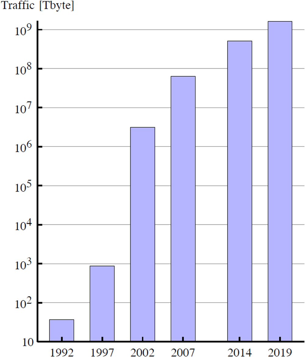
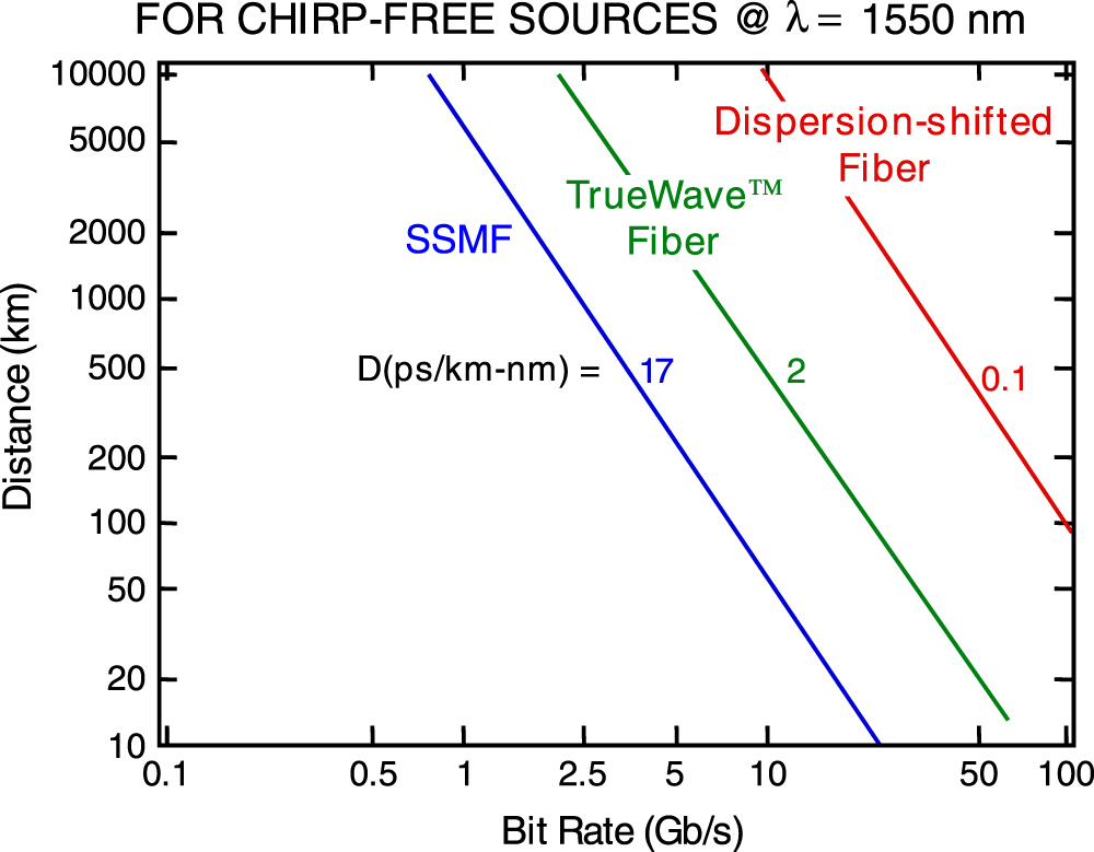
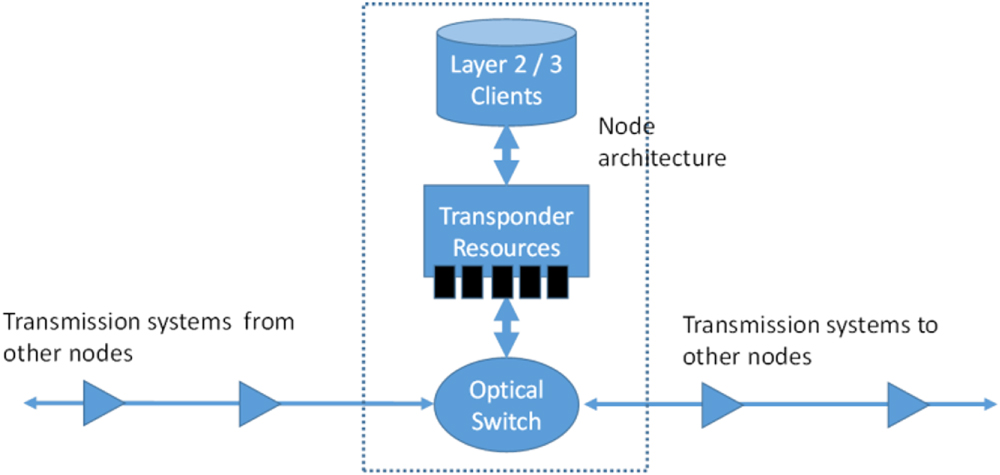
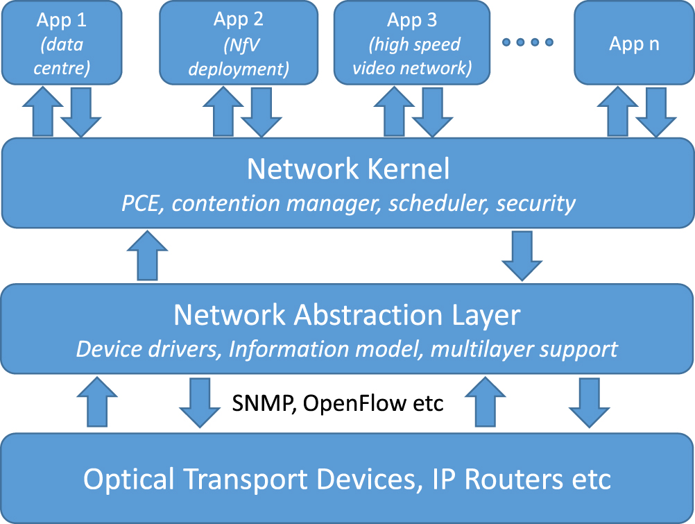
Figure 25. Schematic of a small quantum communication network with three parties labeled A, B and C. The quantum memories allows for synchronization of the quantum network, and the qubit amplifier allows one to overcome losses (only necessary for so-called device-independent applications).
Download figure:
Standard image High-resolution image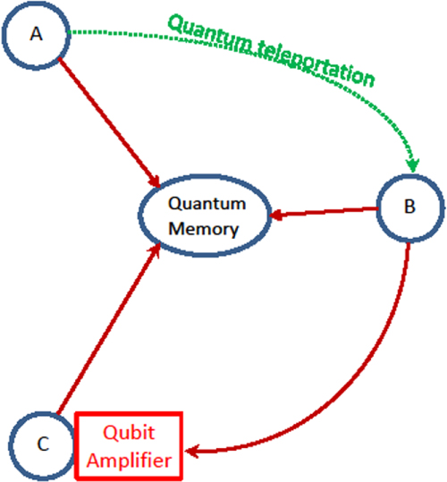
Current and future challenges
QC faces many challenges that range from industrializing quantum technologies to conceptual questions in theoretical physics, spanning various fields of physics, from optics to material science.
Sources: Besides the relatively simple case of point-to-point QKD all QC tasks require sources of entangled photons. Today such sources are based on spontaneous parametric down-conversion, hence are probabilistic. Consequently, in order to avoid multiple pairs of photons, the probability of a single pair is maintained quite low, typically 1% to 0.1%. Moreover, coupling losses between the nonlinear crystals in which the photons are created and the optical fiber are critical. A grand challenge is thus to develop handy and deterministic sources of entangled photons.
The quantum channels could be either free space or an optical fiber. The former is mostly convenient for earth-to-satellite and satellite-to-satellite QC; there, the main challenges are the size and weight of the telescopes [162]. For the fibers, the main challenge is losses. Today's best fibers have losses as low as 0.16 dB/km, i.e. after 20 km almost half the photons are still present, see section 3 [163].
Quantum teleportation: This fascinating process allows one to transfer quantum states (i.e. quantum information) using pre-established entanglement as a channel [161]. The quantum state does not follow any trajectory in space, but is 'teleported' from here to there. In addition to the distribution of entanglement, teleportation requires joint measurements, another quantum feature non-existing in classical physics. Joint measurements allow one to measure relative properties between two systems, like 'are your polarization states anti-parallel?', without gaining any information about the individual properties [164]. Hence, the individual properties don't get disturbed, but the correlations between the properties of the two systems get 'quantum correlated', i.e. entangled. In practice, two photons get mixed on a beam-splitter. This works, but requires high stability as the two photons must be indistinguishable in all parameters. In particular timing issues are serious, especially when the photons travel long distances before meeting on the beam-splitter. Moreover, the process is probabilistic and works at best half the time (but one knows when it worked) [165]. A grand challenge is to greatly improve joint measurements. This requires, probably, to transfer of the photonic quantum states in solids and that the joint measurement is carried out on the degrees of freedom that code the quantum state in the solid, e.g. between two spins. Also, from a purely theoretical standpoint, better understanding of joint measurements, like the abstract formulation of non-local correlations, is much in demand.
Heralded probabilistic qubit amplifier should also be mentioned. This process, inspired by teleportation, allows one to increase the probability of the presence of a photon without perturbing the qubit it encodes [166]. The challenge is to demonstrate such an amplifier over a long distance (>10 km).
Detectors: QC is mostly done using individual photons, hence the requirement of excellent single-photon detectors. Though it should be said that one can also use so-called continuous variables, e.g. squeezed light pulses and homodyne detection systems [167]. Recently, single-photon detectors have made huge progress, with efficiencies increasing in a couple of years from 10%–20% to 80%–90%, thanks to superconducting detection systems [168]. At the same time, the time-jitter reduced to below 100 ps. Still, there are several grand challenges:
- −simpler/cheaper (in particular higher temperatures, at least 3 K, possibly high-temperature superconductors)
- −photon-number resolving detectors, up to a few tens of photons. This fascinating perspective makes sense, however, only if the detection efficiency is at least 95%
- −and 99%–100% efficiency. This seems feasible.
Quantum memories allow one to convert reversibly and on demand photonic quantum states into and out of some atomic system with long coherence times [169]. They are needed to synchronize complex quantum networks by temporarily stopping photons. They could also turn probabilistic photon sources into a quasi-deterministic one, provided their efficiency is high enough. Today, quantum memories are still in the labs. Although all parameters like storage time, efficiency, fidelity, bandwidth and muti-mode capacity have been satisfactorily demonstrated, each demonstration used a different system. Hence, the grand challenge is to develop one system capable of storing 100 photonic qubits (e.g. in 100 time modes) for one second with an efficiency of 90% and fidelity around 95%. This is an enormous challenge. It is unclear whether the best solution will turn out to use single natural or artificial atoms in a cavity or use ensembles of atoms (gas or doped optical crystals). It requires a mix of material science and chemistry (for the crystals), cryogenics (low temperatures seem necessary for long storage times), spectroscopy and radiowave spin echo techniques, optics and electronics.
Multi-partite entanglement and non-locality: future complex quantum networks will routinely produce multi-partite entangled states whose full power remains to be discovered. Already when only two parties are involved, non-local correlations turned out to be the resource for several remarkable processes, called device independent quantum information processes [170]. Likewise, one can expect quantum correlations in complex networks to open new possibilities that remain to be explored.
QKD: Quantum key distribution is the most advanced application of QC. It is already in commercial use in some nich markets since almost ten years, sometimes running continuously since then [171]. The remaining challenges are mostly industrial and commercial. On the industry side, QKD should become cheaper and much faster (one Gb/s is not unthinkable). On the commercial side, the classical security and crypto communities should be educated, they should understand the potential of quantum physics and that it does not render their know-how obsolete, but complements it: quantum does not solve all problems, but offers guaranteed randomness and secrecy. Hence, it will always have to be combined with classical security and cryptographic systems.
Advances in science and technology to meet challenges
The most significant challenges mentioned above require a combination of photonics and solid-state devices, be it for the deterministic sources, the detectors and the quantum memories, and probably also improved joint measurements. The basic grand challenge lays thus in integrated hybrid systems. Ideally, all these solid-state devices will be pigtailed to standard telecom optical fibers, hence easy to combine in large networks.
Concluding remarks
Future quantum networks will look similar to today's internet. One will merely buy components and plug them together via optical fibers, all driven and synchronized by a higher order control software. Randomness and secrecy will come for free. Entanglement, non-locality and teleportation will be common and children will get used to them. Applications unthinkable today will proliferate. Such a dream is possible thanks to QC.