


Abstract
Helicon current drive (CD), also called fast wave CD in the lower hybrid range of frequencies, has long been regarded as a promising CD tool for reactor grade plasmas. A newly installed MW-level system at DIII-D will be the first test of this technology in reactor-relevant plasmas, in the sense that full single-pass absorption is expected. A 30-module traveling wave antenna has been installed and optimized in-vessel in early 2020. The linear electromagnetic characteristics of the unloaded module array have been extensively tested both on the bench and in the vessel at instrumentation power levels. Excellent performance has been achieved, ∼2% reflected power and ∼1.5% dissipated power per module in air, in a 10 MHz band around 476 MHz. Stripline feeds on both ends of the antenna allow either co or counter CD. The installation of a 1.2 MW klystron and associated high-power electronics was completed in Fall 2020. Commissioning of the antenna is ongoing. An important goal of this experiment is to validate the helicon CD physics basis using an extensive set of new and upgraded diagnostics.
Export citation and abstract BibTeX RIS
1. Introduction
Helicon current drive (CD), also called fast wave CD in the lower hybrid range of frequencies, has long been regarded as a promising CD tool for reactor grade plasmas [1–4]. Steady-state advanced tokamak reactors require non-inductive CD in the mid-radius region, near  ρ ∼ 0.6. DIII-D is currently investigating several methods for off-axis CD [5], i.e. top-launch electron cyclotron CD in 2019–2020 [6], helicon CD planned for 2021–2022, and high-field-side launch lower hybrid current drive (LHCD) [7, 8] to be installed in 2022. In the past, fast waves in the frequency range of 4–10
  ΩD, have been used in DIII-D for core heating and CD (FW H&CD) [9–11]. The term 'helicon waves' refers here to fast waves in the lower hybrid range of frequencies, approximately 4–5 times higher frequency than previous FWCD experiments in DIII-D. At these high frequencies, fast waves have propagation characteristics similar to whistlers, i.e. the group velocity is directed mainly along the background magnetic field. The waves slowly spiral radially inwards, gradually depositing their energy. The slow radial propagation allows strong off-axis absorption. Helicon waves have been suggested for CD in reactor plasmas [1–3], as they are thought to be able to propagate into the core without a density limit [12] from which LHCD suffers. The weaker damping than lower hybrid waves also ensures helicon waves can reach deeper into the plasma and avoid full absorption at the plasma edge. Helicon CD is therefore predicted to be effective at high densities and high electron temperatures. The installation of the new MW-level helicon system at DIII-D enables the first tests of this technology in reactor-relevant plasmas, in the sense that full first-pass absorption is expected. A similar helicon system is also being pursued at KSTAR [13].
The net efficiency of a CD system is of utmost importance for a power plant, as high efficiency translates into less recirculated power, and also drives down the cost of the heating and CD systems required for a reactor. Two important factors in the efficiency are the fraction of the coupled RF power that is absorbed in the core plasma, and the current driven per absorbed unit of power. Wave absorption for helicon and LHCD occurs through electron Landau damping as the subset of electrons with velocity parallel to the static B-field equal to the parallel phase velocity of the wave gain energy from the wave [14]. Parallel Landau damping scales as  (see [4, 15]), where k⊥ is the perpendicular wave number,
  ,
,  , where v∥ is the parallel phase velocity,
  is the electron thermal speed, n∥ is the parallel index of refraction, and c is the speed of light. The factor G(ω, n∥, ξe) is given in [4, 15], with approximations listed in [15]. The amount of current driven by the absorbed power is described by the Ehst–Karney approximate formula [16]
  , defined as the ratio of the driven current density to the absorbed RF power density. The dimensionless factor
  is a strongly increasing function of ξe for ξe ≿ 2. A key parameter for the wave propagation, absorption and CD efficiency therefore is ξe, or n∥ = ck∥/ω for a target plasma with a specified electron temperature. An optimum value of ξe exists since two competing effects are at play: higher ξe leads to better CD efficiency per absorbed power, but on the other hand power absorption decreases exponentially as
  . Scoping studies for helicon waves by Prater et al [4] showed n∥ = 3 at 500 MHz to be optimal for the normalized wavenumber launched by the antenna for the high performance high-beta target plasma. As the wave penetrates the plasma core, n∥ undergoes an upshift to 4–5 at which point the wave is absorbed in plasmas with electron temperature in the ∼4 keV range. GENRAY predictions for the total driven current are in the range of 60 kA at ρ ∼ 0.6 per MW of absorbed RF power. This driven current corresponds to a figure of merit
  (for comparison, LHCD for ITER is predicted to have a figure of merit ηLHCD ≃ 0.17 × 10²⁰ AW−1 m−2 [17]).
The helicon system at DIII-D combines the physics of helicon waves with the technological advances in traveling wave antennas (TWA). The TWA has many advantages, such as load resilience, lower operating voltages on the straps, narrow n∥ spectra, and fewer feed transmission lines than traditional strap antennas. The helicon antenna at DIII-D consists of a TWA of the comb-line type [18–20], pioneered at DIII-D. A similar TWA has been explored at JFT-2M [21, 22], and is being tested at KSTAR [13, 23]. Traveling wave strap antennas are also being envisioned for ICRH on DEMO [24–26] with proof of principle tests coming up on WEST [27].
The present paper describes the concept, design, installation and the first results at low to moderate power of the helicon system at DIII-D. The paper is organized as follows. Section 2 gives an overview of the design and testing of the antenna and in-vessel transmission lines. Section 3 discusses the high-power RF source and ex-vessel transmission line network. Section 4 introduces the diagnostics embedded in the antenna and neighboring plasma facing tiles, as well as diagnostics to be installed in the near-future. Section 5 gives initial results of the system at moderate power. Section 6 discusses the initial experiments planned at high power, followed by the conclusions in section 7.
2. Traveling wave antenna
2.1. Concept and design
The design of the antenna structure needs to satisfy several requirements, most driven by physics, some driven by practical considerations. The requirement for the helicon high-power antenna is to efficiently launch a high-power unidirectional fast wave in the lower hybrid range of frequencies using a low-loss structure. For typical DIII-D parameters, the operating frequency in this regime is in the hundreds of MHz range. The choice of 476 MHz was determined by the availability of a decommissioned B-factory klystron (BFK) from the SLAC National Accelerator Laboratory (see section 3), with a maximum RF output power of 1.2 MW. A picture of the installed antenna in-vessel is shown in figure 1. It is designed to have a narrow parallel normalized wave number spectrum peaked at n∥ = 3. It consists of 30 modules, spanning along the outer wall approximately 1.5 m toroidally and 20 cm poloidally. The modules are tilted to align with the background magnetic field in the high-beta target scenario which uses off-axis NBI heating, requiring 'reversed' BT and 'standard' IP to optimize the CD by the off-axis tilted beam line. Note that the four-strap ICRH antenna has the opposite Faraday screen tilt, as it was optimized for the 'standard' BT and IP direction in DIII-D. Each module has current straps, capacitor plates/rods and is designed to be resonant at 476 MHz. The antenna can be fed from either side to allow either co- or counter-CD. Power is transferred toroidally along the antenna through mutual reactive coupling from one module to the next with low losses.

Figure 1. The DIII-D helicon antenna (center of picture) consisting of 30 individual modules, spanning approximately 40 degrees toroidally along the outer wall. The modules are tilted to align with the direction of the magnetic field for the target plasma scenario (reversed toroidal magnetic field Bt, forward plasma current IP).
Download figure:
Standard image High-resolution imageThe main characteristics of the comb-line type TWA can be illustrated with a simple lumped element circuit model [13, 20], as shown in figure 2. Each module is represented by a resonant circuit with inductance  L, capacitance C and resistance
  Rt. The modules are coupled to their neighbors through their mutual inductance
  M. The total dissipated power in each module is the sum of the power radiated to the plasma and the power dissipated in the form of ohmic heating. The losses are represented in the model by the resistance
 Rt = RC + RP, with RC representing the conductors' resistance and ohmic losses in the modules, and the loading resistance, RP, indicating the power coupled to the plasma. The circuit equations can be written as follows,


where S is given by

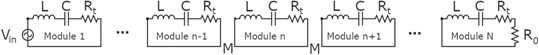
Figure 2. Lumped element circuit model of TWA, consisting of N individual modules. Each module is a tuned LRC circuit. Power is transferred down the array through the mutual inductance M.
Download figure:
Standard image High-resolution imageThe resonant frequency of the system is given by  . As a consequence, near the resonant frequency the term S reduces to the purely resistive terms
  Rt. In the normal operation of the antenna, the condition Rt ≪ ω0
M applies such that most of the power is transferred from one module to the next, with only a small fraction being radiated to the plasma or lost as ohmic heating at
Rt. In the normal operation of the antenna, the condition Rt ≪ ω0
M applies such that most of the power is transferred from one module to the next, with only a small fraction being radiated to the plasma or lost as ohmic heating at  ω ≃ ω0. Even though the RF power coupled to the plasma per module may be small, the large number of elements in the array ensures most of the input power incident on the first module is coupled to the plasma, as long as the loading resistance RP is much larger than the ohmic resistance
  RC. A major benefit of the comb-line TWA is its resilience to changes in plasma loading. The input impedance is largely determined by the mutual inductance
  M, to the extent that plasma-induced changes to the mutual inductance are small. This eliminates the need for a dynamic antenna matching network.
In equation (1), Vin denotes the RF source voltage in the feed-module, while R0 ≃ ω0
M represents the resistive load at the end of the array in equation (3). Any power not lost through ohmic dissipation nor coupled to the plasma will exit the antenna array and be dissipated in the load R0. An alternative option is to recirculate the undissipated power and feed it back into the first antenna module. This would allow the use of a shorter array since the requirement to have most power dissipated in a single pass through the array is no longer applicable. This option is not implemented in the DIII-D system for the sake of simplicity, reduced cost, and lower peak RF electric field in the structure for a given power level.
Figure 3 shows the modeled voltage reflection and transmission coefficients, as well as the phasing of the array as a function of frequency in the neighborhood of  ω = ω0. The term transmission refers to the power exiting the array, and being dissipated in the load
  R0, i.e. the fraction of the input power that is not coupled to the plasma or dissipated as ohmic losses in the array. This fraction is equal to the square of the voltage transmission coefficient plotted in figure 3. The TWA acts as a band pass filter with a maximum in transmitted power and a minimum in reflected power at mid-band. The bandwidth can be shown to scale as
  . The transmission coefficient is less than 1 due to the ohmic losses and due to plasma loading. The case modeled in figure 3 assumes that out of the power reaching a particular module, 1.5% is lost due to ohmic losses in that module and 6.5% is coupled to the plasma. This results in 92% of the power incident on a module being transferred to the next module. Without a plasma present, no power is radiated by the antenna since the antenna imposes a value of n∥ > 1. Therefore measuring the transmission coefficient without a plasma allows the ohmic losses in the array to be quantified. As shown in section 2.3, the value of 1.5% ohmic power loss per module is determined by measurements. For the modeled array, the transmitted fraction of the input power is 63% without a plasma load, and 8% if the assumed plasma load is considered (where we assumed in this example that 6.5% of the incident power on a given module is coupled to the plasma by that module). In a real experiment, the fractional coupled power by a module, and the total power coupled to the plasma by the array can be determined by comparing the transmission and reflection coefficients of the antenna in the presence of plasma with those in the absence of plasma. Indeed, the waste power, i.e. the undissipated power exiting the array, can be written as (neglecting losses in the transmission lines)

where Pin is the input power to the array, ρ is the voltage reflection coefficient, a is the fractional ohmic power loss per module, and b is the fractional coupled power per module. Pwaste, Pin, and ρ are measured quantities. a is determined in the absence of plasma (when  b = 0), and the knowledge of a (=1.5% for the DIII-D antenna) is then used to obtain b during plasma experiments. The total coupled power and total ohmic losses are then given by


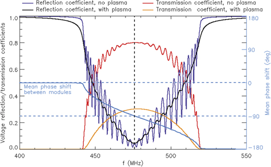
Figure 3. Modeled voltage reflection and transmission coefficients, with and without plasma load in a frequency range near 476 MHz. Also shown is the mean phase shift between modules.
Download figure:
Standard image High-resolution imageFor the case with a plasma load with this assumed level of  RP, 75% of the input power is coupled to the plasma, 17% of the input power is lost to ohmic heating of the modules, and the remaining 8% of the input power exits the array as waste power. The presence of plasma strongly reduces ohmic losses from 36% to 17% since less power reaches each module, with the exception of the feed-module, due to the power being coupled to the plasma.
The antenna phasing depends strongly on the operating frequency, as shown in figure 3. At mid-band the mean phase shift between modules is 90°, with four modules making up one wavelength. The requirement of imposing n∥ = 3, or λ∥ = 21 cm at 476 MHz, is then satisfied by choosing the width and spacing of the modules appropriately. At the low frequency edge of the bandpass region the mean phase shift between modules approaches 0°, i.e. the antenna acts as a monopole. At the high frequency edge of the bandpass region, the mean phase shift between modules approaches 180°, which imposes the highest n∥ (=6 for the DIII-D antenna). These extremes are only of theoretical interest since the reflection coefficient approaches unity at the band-edges, makes these points unsuitable for operation. Nevertheless, with a sufficiently broadband source, a choice of n∥ values between 2 and 4 would be accessible with this antenna. The phasing of the antenna will however not be a free parameter in the high-power experiments since the high-power klystron at DIII-D is only tunable a few MHz around 476 MHz. The dependence of the antenna phasing on frequency has been explored at the 400 W level with a low-power prototype antenna, and was found to perform as expected [20].
2.2. Implementation and installation
The inner workings of a single antenna inner module are shown in figure 4. Each module consists of a poloidal stack of two current straps, each supported in the middle by a grounded pedestal. The straps are connected to capacitor plates on either side (vertical in the picture). A number of movable capacitor rods allow for fine-tuning of the capacitance of each module. The inductance of the straps combined with the capacitance of the capacitor plates and rods essentially make each module a resonant RLC circuit. Each module was tuned to the same resonant frequency to within ±0.5 MHz, and with a quality factor 'Q' in excess of 1000. The straps and capacitor plates/rods are enclosed in a slotted box with Faraday screen rods to protect the modules from the plasma, and to screen out the electric field component parallel to the rods. The modules are mounted in the DIII-D vessel with the Faraday screen rods approximately aligned with the expected pitch of the magnetic field to minimize parasitic excitation of the slow mode. The straps, capacitor plates and rods, and the slotted enclosure are constructed of CuCrZr. The Faraday screen bars are TZM (molybdenum alloy) coated with a thin layer of boron carbide to minimize introduction of high-Z impurities into the discharge. After each module was tuned, the module was brazed to obtain a low-loss structure. After brazing, the resonant frequency of each individual module was re-confirmed.

Figure 4. Single inner module cut-away; the poloidal direction is horizontal in the figure. Each module is 21 cm high in the poloidal direction, 8 cm deep in the major radial direction and 5 cm wide. Reprinted from [29], Copyright (2017), with permission from Elsevier.
Download figure:
Standard image High-resolution imageThe test program evaluated the breakdown thresholds at high RF voltages for a number of prototype helicon components using a 10 kW UHF television transmitter. Tests were performed on multiple module designs and transmission line components [28]. Many tests used resonant circuit designs to produce standing wave voltages of amplitudes equivalent to those produced by ∼1 MW traveling waves. A single strap CuZrCr helicon prototype module fed with a loosely coupled resonator was able to support 22.5 kV cm−1 electric fields, measured with an electric field probe whose response was calibrated using COMSOL modeling of the probe. These fields are similar to the expected maximum electric fields in the high-power antenna at 1 MW of input power, calculated using the QuickWave software package. Testing of prototypes also found that the single-module resonant frequency downshifts by 2 MHz as a module is heated from 30 to 300 °C, an effect caused by the thermal expansion of the capacitive gaps between the module strap and the end wall. These results suggested the requirement of optimal antenna performance in a 5 MHz frequency range around 476 MHz.
In the DIII-D vessel the modules are mounted on six Inconel water-cooled backplates, five modules per backplate. A rendering of the mounting of the modules on a backplate assembly is shown in figure 5. Power is fed from one end of the array and transferred down the array through the mutual inductance between modules. The depth of the slots in the copper enclosure of the modules determines the mutual inductance between modules. The slot depth was increased for the HPHA compared to the prototype LPHA [14], resulting in a roughly threefold increase in the mutual coupling. As a result, the bandwidth of the antenna increased from ∼25 MHz to ∼70 MHz, as shown in figure 6. Other benefits of the increased mutual coupling are lower peak electric fields, more involvement of the downstream modules, and reduced sensitivity of the input impedance to variations in the mutual coupling caused by the plasma.

Figure 5. Rendering of modules mounted onto a backplate assembly. Reproduced with permission from [30].
Download figure:
Standard image High-resolution image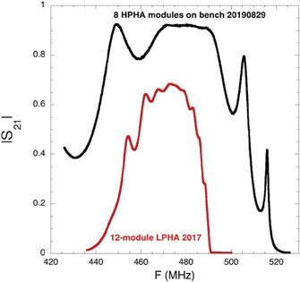
Figure 6. Comparison of the voltage transmission coefficient between the low-power helicon antenna (LPHA) and a bench test of an array of 8 modules of the high-power helicon antenna (HPHA).
Download figure:
Standard image High-resolution imageAt either end of the array, a specialized end module couples input power from a transmission line into the array, as well as couples waste power out of the array into a second transmission line. A schematic of the end module is shown in figure 7. The end modules contain the same current straps and capacitive plates as the inner modules (cf figure 4) and four additional coupling straps, indicated in the figure as the RF feeds connected to ports P1–P4. The RF feed-straps couple power reactively to the main current straps. The distance between the RF feeds and the main current strap can be changed to impedance match the antenna to the transmission line. The four RF feeds are fed with equal power and in a 0π0π phasing to produce unidirectional poloidal current flow on the main current straps. The end modules can each be connected to four separate coaxial feeds, which was done during testing. In the final in-vessel installation the power is transferred to the end modules through a specialized stripline.
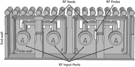
Figure 7. End module with four coupling-straps to transfer power from a transmission line into the array and vice-versa. Reprinted from [31], Copyright (2019), with permission from Elsevier.
Download figure:
Standard image High-resolution imageA picture of the partially installed stripline on one end of the antenna is shown in figure 8. The front cover and the side covers are removed to make the inner components visible. A second stripline is installed at the other end of the array. A coaxial transmission line with characteristic impedance of 25 Ω enters the DIII-D vessel through a vacuum feedthrough (not visible) and connects to the back of the stripline. The inner conductor of the input coax connects to the inner conductor of the stripline, which splits into two RF paths. The extra path length along the top of the stripline introduces a 180° phase shift between the two paths. Note that a ground plane positioned in between the two RF paths is not shown in figure 8 since it had not been installed yet. Each of the two RF paths splits into two equal-power outputs near the end-module. The stripline effectively converts a single high-power input to four equal power outputs with 0π0π phasing, to feed into the end module of the array. The weight of the inner conductors is supported by quarter-wavelength-long shorted stubs on either side of the stripline. The stripline is a complex 3D structure, designed to fit closely to the DIII-D vessel wall. Sections of the stripline inner conductor were manufactured by additive manufacturing techniques in Inconel, and were later plated with copper. During RF testing of the stripline, a local impedance mismatch was discovered that necessitated the use of an ex-vessel tuner. The source of this impedance mismatch has not yet been identified and did not appear in full-scale prototypes of the stripline assemblies. The antenna system is nevertheless expected to be resilient to changes in plasma loading since the impedance mismatch is believed to be inside the stripline, and should not be affected by the presence of the plasma, i.e. the ex-vessel tuner will not need to be adjusted during plasma operations.
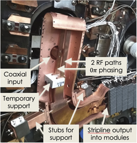
Figure 8. The stripline, partially installed in the photo, has a coaxial input and produces four equal power outputs with 0π0π phasing.
Download figure:
Standard image High-resolution image2.3. Testing and optimization
The linear electromagnetic characteristics of the unloaded module array have been extensively tested on the bench and on a DIII-D mock-up wall at instrumentation power levels, with sub-arrays of 5, 10, 15, 20 and the full array of 30 modules on curved backplates, as well as flat on the bench. A large reflection coefficient observed during initial testing, which did not include the striplines was successfully corrected using an optimization procedure developed and tested on the bench prior to the in-vessel installation. The layout of the modules installed on the back plates, as shown in figure 9, follows a two-module poloidal stagger pattern designed to shorten the toroidal connection length at the face of the antenna and thus minimize plasma density penetrating into the antenna modules. However, this two-module stagger pattern results in a periodicity in the mutual coupling between modules that causes significant reflections in the antenna (∼20% power reflected). Since the nominal phasing between modules is 90° at the operating frequency, any even-numbered periodicity in the mutual coupling between modules causes the reflections in the array to add constructively. Separate tests with a set of 20 modules flat on the bench clearly showed that a two-module periodicity in the mutual coupling along the array results in substantially increased reflections, and associated reduction of antenna efficiency. Adjustment of the inter-module spacing (in the toroidal direction) can compensate for this, as indicated in figure 9, resulting in a more uniform mutual coupling between modules along the entire array, and reducing the reflected power to less than a few percent. The optimization involves minimizing the reflected power and maximizing the transmitted power in a band near the operating frequency of 476 MHz. The optimization procedure consists of re-positioning the modules starting at one end of the array, typically the feed end, until all module positions have been adjusted, and the reflections have been reduced. The antenna array is then fed from the other end, and the optimization procedure is repeated. After a few iterations, the antenna characteristics are optimal when fed from either end.
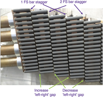
Figure 9. Modules mounted on the backplates, showing the stagger in the poloidal overlap between modules.
Download figure:
Standard image High-resolution imageThe antenna was tested and tuned at instrumentation-power levels during different stages of the in-vessel installation: tests of the installed antenna were done without striplines, with one stripline, and with both striplines and ex-vessel tuners in place. The measured voltage reflection coefficient and voltage transmission coefficients after the antenna, both striplines and ex-vessels tuners were installed are shown in figure 10. The system was fed with a vector network analyzer at the ex-vessel tuners. Data is shown with the antenna fed from the low angle side (LAS) and the high angle side (HAS). After the optimization procedure, the power reflection coefficient of the 30-module array was reduced to ∼1% at 476 MHz, and with less than 4% reflected power in a 10 MHz band. The power transmission coefficient for the 30-module array without the striplines (data not shown in figure 10) in air is 63%, indicating a 36% power dissipation in the antenna, or 1.5% per module. Virtually no power is expected to be radiated into air/vacuum in the absence of a plasma load near mid-band since the imposed parallel wave number is higher than the free-space wave number at 476 MHz. Therefore any input power that does not reach the end of the array must have been resistively dissipated in the structure, not radiated. As outlined in section 2.1, in a scenario with 75% of power coupled to the plasma, the total dissipated power in the modules is expected to drop to 17% of the input power, and with 8% of the input power exiting the antenna as waste power. Strong plasma coupling reduces the power traveling along the array and therefore reduces the total resistive dissipation in the array. As pointed out earlier, the first module still sees nearly the same power dissipation as in air/vacuum, estimated at 15 kW for a 1 MW incident power. Thermal modeling of the antenna has shown that the cooling of the antenna is adequate to permit 6 s-long 1 MW pulses every 12 min, which is the maximum practical DIII-D shot rate.
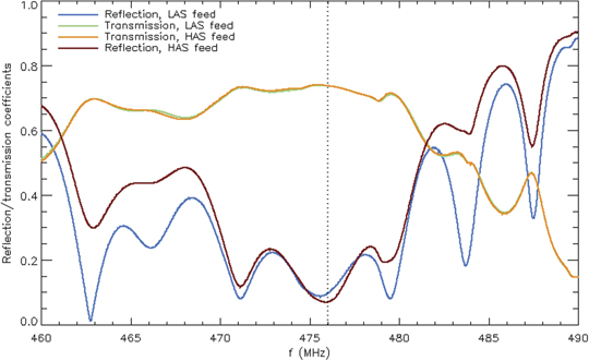
Figure 10. Voltage reflection and transmission coefficients near 476 MHz, for the antenna installed in-vessel with both striplines and ex-vessel tuners in place. Results are shown with the antenna being fed from the LAS and the HAS.
Download figure:
Standard image High-resolution imageAntenna data was also acquired in-vessel with a pick-up loop placed near the Faraday screen (see figure 11). Both the amplitude and phase of the magnetic field in front of each module along the array was recorded in the frequency band of interest. Ideally, the amplitude decays exponentially from the fed end, and the phase difference at 476 MHz between two consecutive modules should be constant along the array and equal to 90 degrees. Large variations in the amplitude and phase are indications of a substantial standing mode component in the array. Maximizing directional wave launch requires minimizing standing modes. Figure 12 shows the probe data acquired in-vessel. The top panel of figure 12 displays the measured phase advance between two consecutive modules at 476 MHz. The phase shifts are uniform along the array, and have the opposite sign when the array is fed from the other end. The middle panel shows the accumulated phase along the array, i.e. the cumulative sum along the array of phase changes between modules, again with opposite slope when the array is fed from the other side. The top two panels clearly show the directionality of the wave propagation in the antenna. The probe amplitude, shown in the bottom panel, decays away from the feed point, and has only small fluctuations indicating no significant standing waves are present. It is important to note here that the antenna behaves very symmetrically when feeding from either end of the array, which is also evident from the reflection and transmission coefficients shown in figure 10. This is crucial for the planned experiments in order to allow the choice of either co- or counter-CD phasing.
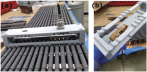
Figure 11. Pick-up loop probe used for bench testing and in-vessel measurements.
Download figure:
Standard image High-resolution image
Figure 12. Phase and amplitude along array as measured with a pick-up coil in-vessel, with the antenna powered from the LAS and the HAS.
Download figure:
Standard image High-resolution image3. RF source and transmission line network
The RF source consists of a single B-Factory klystron [32] that operates at 476 MHz and is able to produce a maximum RF output power of 1.2 MW. The klystron and its high-voltage power supply were obtained from SLAC, and adapted with a new control system suitable for pulsed mode operation on DIII-D. A schematic of the RF system is shown in figure 13. The high-voltage power supply accelerates electrons from a heated filament, producing an electron beam that is guided through 7 RF cavities by the klystron magnetic field. Typical beam voltages and currents at nominal output power are 83 kV and 24 A or 2 MW of beam power. The klystron is driven by a gated RF source at 100 W, and modulation of the klystron output RF power can be achieved by modulating the RF drive power and/or the high voltage. No modulation anode is required. After passing through all 7 cavities, the remaining electron beam power is deposited onto a collector, which can withstand the full 2 MW of beam power for 0.5 s when no RF is present. A circulator is located at the klystron RF output port to protect it from reflected power. The klystron has a 1 dB bandwidth of ±1.5 MHz around 476 MHz and has an effective efficiency of 60% at the saturated output power of 1.2 MW.
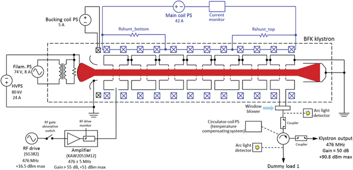
Figure 13. Schematic of the high-power RF source.
Download figure:
Standard image High-resolution imageA schematic of the transmission line network is shown in figure 14. The RF output of the klystron is routed through the circulator to a 9'' coaxial feed line, which then connects to a four-port waveguide switching network, located just outside the machine pit wall. Any reflected power returning from the switch toward the klystron will be diverted by the circulator into a 9'' coaxial reject line and dissipated in a 50 Ohm dummy load (labeled 'dummy load 1'). The four-port switch can be configured to send power directly to a second dummy load (labeled 'dummy load 2') for klystron conditioning. During normal operation the switch sends power either to the high-angle-side (HAS) or the low-angle-side (LAS) of the antenna through a 6'' 25 Ω coaxial line. The 6'' line contains both DC outer–outer breaks and DC inner–inner breaks (omitted in the diagram) that provide up to 15 kV of DC isolation between the DIII-D vessel and the rest of the transmission line. The 6'' line then connects via a vacuum feedthrough to the striplines and the antenna. Any power injected at one port that is not coupled to the plasma or dissipated in the antenna structure leaves at the other port, and is dissipated in dummy load 2 after passing through the four-port switch and a 9'' waste line. The inset of figure 14 indicates where the RF input power is directed for different settings of the waveguide switches. Directional couplers at various places along the transmission line quantify the line losses, the antenna waste power and reflected power.
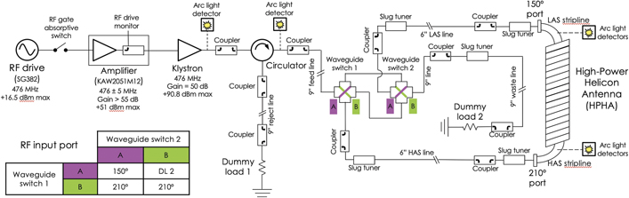
Figure 14. Schematic of the transmission line network, not to scale.
Download figure:
Standard image High-resolution imageSignificant efforts have gone into improvement of the performance of the high-power transmission line network. Tests of sections of the transmission lines revealed power reflection coefficients in the 20% range for some sections. Originally (c. 1992) the coaxial lines used ceramic insulating supports ('pins') for the inner conductor. These ceramic pins were replaced by quartz pins in 1994 in order to increase the RF high-voltage standoff during ion cyclotron range of frequencies experiments in the 60–120 MHz range. However, bench testing at the helicon operating frequency range (476 MHz), showed that these quartz support pins can cause significant reflections, particularly in the elbow sections (90° bends). Bench tests comparing coaxial sections with ceramic pins versus quartz pins confirmed that while sections with ceramic pins do not exhibit large reflections, sections with quartz pins showed important power reflections that scale roughly as the square root of the number of elbows in the line. The replacement of the quartz pins by ceramic pins in the elbows in the 9'' diameter coax significantly lowered the power reflection coefficient to values in the 1% range around 476 MHz.
4. Diagnostics
The antenna is equipped with a suite of diagnostics shown in figure 15. Eighteen RF probes (stars in figure 15) are embedded in a subset of the 30 modules in the array. The RF probes are placed in a recess in the pedestal of the modules, as indicated in figure 4. Each probe is a single-turn loop fitted with a stainless-steel cylindrical cap with a narrow slit that limits the magnetic flux onto the coil, and thereby reduces the power levels in the probe to acceptable levels (an attenuation of roughly 70 dB). The RF probes are placed in groups around the antenna, marked with stars in figure 15. The end modules each have two probes, one behind the upper straps, and another behind the lower straps, to verify that both sides of the end-modules are fed in phase and with equal power. Any imbalance in the antenna feed would be detected by these probes. The remaining RF probes are distributed along the array in groups to provide measurements of phase and amplitude measurements along the array. The RF probes will initially be used to confirm the antenna has the correct phasing, and to quantify the loading of the antenna array (in addition to loading measurements obtained from ex-vessel directional couplers at both ends of the antenna outputs). At a later stage these probe measurements are planned to be incorporated into an RF-based arc detection system. Six fixed Langmuir probes were installed in tiles around the antenna to measure edge plasma density as well as to provide a secondary capacitive RF measurement; two probes are in tiles near the low-angle stripline, two are in tiles near the middle of the antenna, and two are in tiles near the high-angle stripline. The striplines are equipped with three fiber optic arc detectors to detect light flashes in the stripline due to arcs during operation of the antenna. 39 thermocouples are embedded in the antenna and surrounding tiles, with their locations indicated in figure 15. A visible light camera and an infrared (IR) camera were added to the diagnostics with a nearly full view of the antenna modules. The IR camera is live-streamed to the control room. For each discharge a 30 s video of the IR camera view is stored on a server.
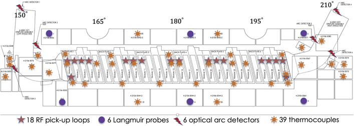
Figure 15. Installed diagnostics in and around the helicon antenna.
Download figure:
Standard image High-resolution imageSeveral new and upgraded diagnostics are planned and under development for the helicon program. A set of local gas injectors with spectroscopic observation to both sides of the antenna will enable the measurement of the electron density and temperature adjacent to the antenna by beam emission spectroscopy. In situ cold cathode WISP gauges will be used for measurement of fractional impurity neutral abundances. A laser-based technique known as Doppler-free saturation spectroscopy [33, 34] will be implemented to measure the helicon wave electric field vector over a 2D region of space in the edge of the plasma. The wave electric field vector is obtained by fitting the Schrodinger equation to Doppler-free Dβ spectra. This technique results in an accuracy of better than 10 V cm−1, nearly two orders of magnitude greater than that of previous work. For far-field wave measurements, the existing phase contrast imaging (PCI) diagnostic [35] is being upgraded with a heterodyne detection system able to detect fluctuations at 476 MHz. The PCI diagnostic considerably reduces the geometrical complexity of detecting the wave from three to two dimensions because, by virtue of its line integral along the vertical direction, it suffices to intercept the helicon trajectory at any value in the vertical direction. Extensive ray tracing calculations on a number of past DIII-D discharges show that the PCI, in its current location, is expected to intercept the trajectory of the helicon wave in plasmas with parameters suitable for off-axis CD. Using values for the wave electric field estimated by full-wave modeling work, it is expected that the PCI will be able to measure the spatial structure of perturbed density with favorable signal-to-noise ratio.
5. System testing at moderate power
Prior to applying the first RF power to the antenna, various interlocks were tested during the plasma startup phase. A plasma proximity interlock initiates a controlled plasma shutdown if the plasma separatrix-antenna distance drops below a programmed level. Similarly, a controlled plasma shot shutdown is initiated were the IR camera to detect a temperature of over 300 °C anywhere on the helicon antenna modules. Thermocouple data is used to prevent the start of the next plasma shot sequence if the helicon modules have not cooled down sufficiently following a previous shot.
Tests of the antenna have been carried out in vacuum at moderate powers, up to 5 kW, using a separate UHF television transmitter. A power scan of the transmission coefficient is shown in figure 16 for operation at high vacuum, both with and without applied magnetic field, and for operation at atmospheric pressures. In the linear regime, the voltage transmission coefficient is 0.7 (see also figure 10 at f = 476 MHz), which means 50% of the input power exits the antenna and striplines. When operating into high vacuum without a background magnetic field, the system remains in the linear regime only for input powers below 200 W. Above this threshold a rapid drop in the transmission is observed, with only about 5% of the 1.5 kW input power exiting the antenna and striplines. This nonlinear behavior is thought to be caused by multipactoring in the antenna modules that absorbs the RF incident power. Subsequent power scans in air at atmospheric pressure, a condition where multipactoring is not possible, did not show nonlinear behavior. Theoretically, one expects that a static magnetic field could mitigate the multipactor discharge formation by disrupting the bounce resonance of the multipactor effect, if the electric fields are perpendicular to the static magnetic field and the electron gyroradius is smaller than the relevant electrode spacings, which are on the order of a cm. The secondary electron emission yield typically peaks for electrons with energies on the order of 100–200 eV. In that case, the order of magnitude of the critical magnetic field should be ∼100 G. The power dependence of the transmission coefficient in vacuum was measured with low levels of toroidal field and indeed a few hundred Gauss field had a strong effect in extending the range of power levels at which linear behavior is observed by a factor of about 3 or 4. Higher magnetic fields will aid in mitigating multipactor of higher energy electrons, but note that multipacting is still possible along the field lines.

Figure 16. Dependence of transmission coefficient on the input power, for operation at high vacuum with and without magnetic field, and for operation at atmospheric pressure.
Download figure:
Standard image High-resolution imageSubstantial heating due to multipactoring was also observed in the antenna after applying 5 kW to the antenna for several minutes. IR camera images showed that heating is initially localized to the first module on the fed side of the antenna (figure 17(a)). Over the course of many minute-long RF pulses, heating starts spreading gradually to modules further down the array as shown in figure 17(b). This is taken as a sign of conditioning of the modules; as the first module conditions, the power is absorbed and/or reflected there, and little power propagates further along the array. After the first module is conditioned, power is transferred to the next modules, which then show increased heating. Conditioning of the antenna at hundreds of kW with the klystron is ongoing at the time of this writing.

Figure 17. IR camera images of the antenna modules during conditioning at 5 kW, (a) at start of conditioning, (b) after several conditioning sessions.
Download figure:
Standard image High-resolution image
Preliminary tests of the antenna powered at 100 W into plasmas showed strong coupling to the plasma, in excess of 80% of the power applied to the fed end, with almost no power exiting the antenna as waste power. The plasma coupling responded to jogs of the radial position of the plasma as expected, with increased coupling when the separatrix is brought closer to the antenna, similar to what was observed with the low-power prototype antenna [20]. The reflected power fraction measured at the RF source increased slightly during plasma operation, but stayed below 5% in all cases, even during L/H mode transitions, demonstrating the resilience of the antenna input impedance to changes in the plasma loading.
6. Planned experiments
Initial experiments with the helicon system focus on determining the coupling efficiency of the antenna at high power under various plasma conditions, as well as establishing antenna performance in preparation of high-power experiments. Comparisons of measurements of the antenna–plasma coupling to theoretical expectations are fundamental in establishing that the expected wave is being excited in the plasma and to quantify the wave power in the discharge. The same methods that were used in the low-power helicon experiments [20] will be utilized in the high-power experiments. In order to evaluate nonlinear effects, the experimental plan also includes searches for power-dependent loading, studies of the effect of the RF power on the plasma edge density profiles, and monitoring of the frequency spectrum of RF waves in the plasma to study parametric decay instabilities [36].
The power deposition profiles will be experimentally determined to validate ray tracing predictions for helicon waves. The total power absorbed in the plasma is needed to quantify the CD efficiency (driven current per core-absorbed watt), and also to gauge if any significant edge losses are present. The principal absorption mechanism is Landau damping on thermal electrons which are thermalized on a short time scale. By amplitude-modulating the klystron power the deposition profiles can be determined from localized measurements of the modulated electron temperature.
The phenomenon of CD is a more sensitive measure of the interaction in velocity space between electrons and helicon waves than absorption. For example, the CD efficiency has a strong dependence on the parallel index of refraction and directionality of the waves. Fokker–Planck codes constitute a complete model of this wave–particle interaction, but experimental validation of the physics is needed. This is best accomplished by comparing a local measurement of the current density driven by helicon waves to the theoretical computations. The CD profiles are determined from measurements of the internal magnetic field structure, typically using the motional Stark effect diagnostic, which yields both the total parallel current density J∥ and the parallel electric field E∥. The non-inductive current is obtained by subtracting off the inductive component, i.e.
  J∥,NI = J∥ − σneo
E∥. The contribution from helicon waves is distinguished from other non-inductive CD sources by comparing two similar discharges with co-plasma current and counter-plasma current injection of the helicon waves. Taking the difference in J∥,NI between the two discharges allows the helicon wave CD profile to be isolated since all other sources of non-inductive current will cancel.
J∥,NI = J∥ − σneo
E∥. The contribution from helicon waves is distinguished from other non-inductive CD sources by comparing two similar discharges with co-plasma current and counter-plasma current injection of the helicon waves. Taking the difference in J∥,NI between the two discharges allows the helicon wave CD profile to be isolated since all other sources of non-inductive current will cancel.
7. Conclusions
Major elements of the design, construction, installation and commissioning of the helicon CD system on DIII-D have been successfully completed. These have resulted in a system demonstrating excellent RF performance with low reflected power, low losses and good antenna directivity, and with the ability to launch RF power in either the co- or counter-plasma current direction. The system will enable experiments to determine the non-inductive current profile in high-beta discharges, will shed light on the efficiency of a helicon system to drive current off-axis in steady-state tokamaks beyond ITER, and will provide tools to extend DIII-D's steady state research to higher pressure and density.
Disclaimer
This report was prepared as an account of work sponsored by an agency of the United States Government. Neither the United States Government nor any agency thereof, nor any of their employees, makes any warranty, express or implied, or assumes any legal liability or responsibility for the accuracy, completeness, or usefulness of any information, apparatus, product, or process disclosed or represents that its use would not infringe privately owned rights. Reference herein to any specific commercial product, process, or service by trade name, trademark, manufacturer, or otherwise does not necessarily constitute or imply its endorsement, recommendation, or favoring by the United States Government or any agency thereof. The views and opinions of authors expressed herein do not necessarily state or reflect those of the United States Government or any agency thereof.
Acknowledgments
This material is based upon work supported by the U.S. Department of Energy, Office of Science, Office of Fusion Energy Sciences, using the DIII-D National Fusion Facility, a DOE Office of Science user facility, under Awards DE-FC02-04ER54698, DE-AC05-00OR22725, DE-AC02-09CH11466, DE-NA0003525, DE-SC0019256, DE-SC0013911, DE-SC0020284.