


Abstract
The first wall is one of the key components in a tokamak, in particular, for DEMO in the future. The conceptual first wall for a DEMO reactor is designed, fabricated and tested in this paper. It has a sandwich-like structure, which consists of a reduced activation ferritic/martensitic (RAFM) substrate, an interlayer and a plasma-facing material of tungsten produced by chemical vapor deposition (CVD-W) due to its characteristics of high density, high purity and superior thermal shock resistance. The interlayer is required to not only have good adhesion between CVD-W and the CLF-1 substrate, which is a type of RAFM developed by the Southwestern Institute of Physics, but also the capability of tritium transport prevention due to the great importance of controlling the tritium buildup in the first wall, improving the fuel efficiency and conforming to the safety regulations of tritium. Titanium nitride (TiN), a well-known tritium barrier, is selected as the interlayer material in this work. In total, eight sandwich-like first wall samples have been fabricated, and thermal cycle tests and plasma exposure tests are implemented. The results of material analysis show that the quality of the TiN coating layer is critical for good adhesion and tritium prevention. At the defects of the TiN interlayer, fluorine (F) penetrated into the CLF-1 during the CVD-W fabrication and, as a result, the sandwich-like structure was broken near the CLF-1 side. For some samples, the TiN interlayer made by CVD has sufficient adhesion as an interlayer between CVD-W and CLF-1 during tests so far. These encouraging test results support further examination of TiN as an interlayer material for W on an RAFM steel as a first wall material. Preliminary results indicate that the design and fabrication of the conceptual first wall are feasible. Further tests, including the improvement of the interlayer quality and the tritium permeation test, are necessary in the future.
Export citation and abstract BibTeX RIS
1. Introduction
The first wall, which directly faces the plasma and experiences energetic particles, neutron radiation and steady-state heat loads, as well as transient heat loads such as edge localized modes (ELMs), is one of the key components in a fusion reactor. For a DEMO reactor, the first candidate material of plasma-facing materials (PFM) is tungsten (W), and the current applicable structural material is a reduced activation ferritic/martensitic (RAFM) steel [1]. The heat load on the first wall is much lower than that on the divertor plates. As a result, W-coated material instead of bulk W is promising on the first wall. Moreover, since W has 200 times greater electrical conductivity than graphite, which is the PFM widely used in current tokamaks over the world, larger halo currents and eddy currents will be generated during plasma discharges and the electromagnetic forces on the first wall will be quite big for the bulk W. Also, W has 8.5 times greater mass density than graphite and thus has a larger gravity load. So, taking the physical environments and economical requirements into account, a thick W coating is considered to have obvious advantages for the first wall of DEMO. Since chemical vapor deposition W (CVD-W) has higher density, lower porosity and better thermal shock resistance than other W coatings [2, 3], it is appropriate to apply thick a CVD-W coating as the PFM of the first wall for DEMO. The Southwestern Institute of Physics (SWIP) has already developed a new RAFM material, which is called CLF-1 [4]. The new conceptual first wall for DEMO in this work is designed and developed with CVD-W and CLF-1.
Since the thermal expansion coefficients of W and the RAFM steel are quite different, CVD-W will detach from the CLF-1 steel under heat loads and plasma exposure if it is coated onto CLF-1 directly. As a result, an interlayer must be applied to mitigate the stress between the CVD-W coated layer and the CLF-1 substrate.
Another primary concern on the first wall in DEMO is tritium accumulation in plasma-facing areas. Based on the requirements of tritium self-sufficiency and safety regulation of tritium, it is very important to control the buildup in plasma-facing components (PFCs) (i.e. the first wall) and decrease the tritium inventory [1, 5]. A tritium barrier is one of the crucial technologies to achieve fuel self-sufficiency and safety requirements, but many investigations have been focused on the tritium permeation barriers in the breeding blanket and pipes in the external fuel cycle in a reactor. Due to the high mobility, which means diffusivity here, of hydrogenic species in W, tritium will penetrate into the bulk structure of the first wall and pass through the W PFM, which will cause tritium buildup in PFCs or loss via the cooling channels. Furthermore, the PFM (W) will generate cracks under steady state and transient heat loads and neutron radiation in a reactor. Although W has low permeation, which is the product of diffusivity and solubility, for hydrogen isotopes, due to its very low solubility, as shown by the Area Defect Model [5], cracks in the W will make tritium penetrate into the substrate rapidly. Investigations have shown that cracks will constantly be created and no saturation in crack propagation is found [6]. The tritium will escape from the fuel cycle and will not contribute to the energy production. As a result, when the interlayer between CVD-W and the CLF-1 substrate also works as a tritium barrier with the function of prevention of tritium permeation, it will be greatly beneficial for controlling the tritium accumulation, maximizing the fuel efficiency, reducing the tritium inventory and assuring the fuel self-sufficiency and safety of a DEMO reactor, which must make its own fuel for steady-state operations.
In this paper, a conceptual first wall with the capability of tritium prevention for DEMO is designed. CVD-W is used as the PFM and CLF-1 is the material of the bulk structure. An interlayer which can bond the PFM to the substrate and also behaves as a tritium barrier is also applied and investigated. This work focuses on the conceptual design of the first wall structure and its preliminary tests in order to evaluate the feasibility of the design. It does not deal with the engineering design and tests on a first wall for DEMO. The behavior of the PFM W of the conceptual first wall will be mentioned, but the validation and investigation of the W material are not the goal of this work.
2. Design of the first wall for DEMO
2.1. The structure of the conceptual first wall
The conceptual first wall has a typical sandwich-like structure, as shown in figure 1, which consists of the PFM CVD-W, a bulk substrate of CLF-1 and an interlayer between them.

Figure 1. A schematic of the conceptual first wall.
Download figure:
Standard image High-resolution imageAs the PFM of the first wall for DEMO, it is necessary to have a high melting point, high thermal conductivity, low sputtering yield and low fuel retention, as well as good performance under high steady state and transient heat loads. Many investigations have proved that W is considered to be the only candidate for PFMs so far [7, 8]. Due to the low sputtering yield of W and the intermediate heat load lower than 5 MW m−2 on the first wall by reference to the blankets of ITER, CFETR and others [9–12], it is fitting to apply a thick layer of W onto the first wall. Thick CVD-W with a high purity of 99.9999 wt% and a density of 19.2 g cm−3 has been manufactured by SWIP and the Xiamen Tungsten Company, and presents a high thermal conductivity and good thermal shock resistance [2, 3]. It can be deposited up to 2 mm thick at a deposition rate of 0.5–1 mm h−1. Based on the fluence of energetic particles and heat loads expected on the first wall, a CVD-W layer of 1–2 mm is also what is required, while alleviating the dead load and electromagnetic load of the first wall. In this work, samples with a CVD-W layer of 1 mm in thickness are fabricated.
Many kinds of RAFM steel have been proposed and investigated as the structural material for fusion devices. Alloying additions in RAFM are controlled to bolster structural properties while minimizing activation by reducing the Co, Nb, Ni and Mo contents. CLF-1 (Cr 9.0, C 0.11, Mn 0.6, W 1.6, V 0.3, Ta 0.1, and Fe) has been developed by SWIP and has similar mechanical properties to other RAFMs, such as EUROFER97 in the European Union (EU) and F82 H in Japan [4]. For the purpose of validating the design only, the thickness of the bulk CLF-1 in the conceptual first wall is 5 mm.
Since there is a big difference between the thermal expansion coefficients of CVD-W and CLF-1, which are 4–5  10−6/°C for CVD-W and 10.9–13.2
  10−6/°C for CLF-1 in the temperature range of 200 °C–1000 °C [2], an interlayer is required to mitigate the stress between them. To achieve good adhesion without any delamination or cracks, it is necessary to use a material with an intermediate thermal expansion coefficient in comparison to those of CVD-W and CLF-1.
As the first wall of DEMO, it will work within the temperature range of 300 °C–500 °C [1, 9, 11–14]. The PFM also experiences a high fluence of particles and transient heat loads due to transient events during the operation of a fusion reactor. Therefore, the interlayer must be stable at the working temperature and have good performance under a high temperature gradient and thermal cycling.
Another concern for the interlayer is the capability of prevention of tritium permeation due to the great importance of controlling the tritium buildup in the first wall, improving the fuel efficiency and conforming to the safety regulations of tritium. The requirements of the tritium barrier are quite different from those for the tritium permeation barrier inside the blanket module or the tritium plant. The interlayer here has to suffer high neutron radiation in the order of tens of dpa [1] and the implantation of energetic deuterium and tritium, which could cause excessive retention and permeation due to the cracks and defects induced by neutron radiation and thermal cycles.
Overall, the interlayer is required to have good bonding properties and tritium prevention, which is crucial for assembling the first wall, controlling the inventory buildup and maximizing the fuel efficiency. The candidate interlayer must satisfy: (1) a suitable thermal expansion coefficient which matches the expansion coefficients of CVD-W and CLF-1; (2) good bonding properties for both W and CLF-1; (3) good performance under the working temperature and thermal cycles; (4) excellent properties for prevention of the tritium permeation; (5) acceptable thermal conductivity; (6) good properties after neutron irradiation.
2.2. Design of the interlayer
The interlayer is designed in terms of the requirements described above. Since investigations on tritium barriers have been performed for years and many results can be found easily [5, 15–18], it will be efficient if we select those materials with suitable thermal expansion coefficients from the tritium barriers which have been validated by previous works.
A lot of materials, including metals, oxide, nitride, carbide and so on, can be used as a tritium barrier on a steel bulk. Usually, the interlayer consisting of Ti or Ni has good adhesion strength with the W and steel. Ti is not good as an interlayer since it will react with WF6 during the following fabrication of W by CVD. Ni is not a good tritium barrier due to its high activation after neutron irradiation.
Ceramics are typically considered to be good tritium barriers due to their hydrogen isotope permeabilities, which are typically much lower than those in metals. Oxides are not chosen here due to the activation after neutron radiation and the bad compatibility with plasmas. Among different carbides, titanium carbide has been tested as a tritium barrier [15, 19, 20]. But it is bad here because of the adhesion problems with direct deposition on a steel [5, 15, 19, 20]. Silicon carbide is a promising coating layer under neutron radiation for fusion reactors [21] due to its high radiation resistance, high thermal conductivity and excellent mechanical properties, as well as stability at high temperatures [16, 17, 22, 23]. Although the hydrogenic diffusivity in SiC is many orders of magnitude lower than W [5, 24–26], the thermal expansion coefficient of SiC is 3.4–5  10−6/°C within the temperature range of 200 °C–1000 °C, which is lower than those of both CVD-W and CLF-1. Therefore, it is not suitable for mitigating the stress between CVD-W and CLF-1.
For nitrides, TiN has been studied widely as a barrier due to its good adhesion and the ease of deposition [18]. Its thermal expansion coefficient is 9.35  10−6/°C, which pairs with the coefficients of CVD-W and CLF-1 very well. Additionally the TiN coatings on the 316 l steel and F82 H have been shown to give good adhesion [15, 27, 28]. As a result, TiN is selected as the material of the interlayer, as shown in figure 1.
The thickness of the interlayer has a strong effect on the residual stress inside the coating layer. The higher the thickness, the higher the stress. To mitigate the residual stress and thermal stress of the interlayer under working conditions, the thickness of the interlayer was chosen to be 1 µm.
3. Fabrication
The conceptual first wall for DEMO consists of the substrate bulk of CLF-1, the plasma-facing surface of CVD-W and the TiN interlayer as a tritium barrier and a bonding layer between the substrate and the PFM.
CLF-1 has been developed as a structural material by SWIP and has been tested since 2003, and a 350 kg chunk of CLF-1 steel has been produced [4]. Part of it was cut into samples with the dimensions of 13 mm  13 mm
13 mm 5 mm for coating the TiN interlayer and W material. The CLF-1 samples were mechanically polished before the TiN was coated on the bulk substrate.
The interlayer in the first wall design for DEMO is the crucial part. The TiN coating technology has been investigated for many years and tested successfully [15, 18, 27, 28]. A TiN layer of 1 µm thickness was deposited by CVD onto the CLF-1 substrate with the reactive gases of TiCl4, N2 and NH3 at 900 °C after the substrate bulk was polished and cleaned.
The dense and high purity W coated by CVD with a deposition rate of 0.5–1 mm per hour has been developed over several years at Xiamen Tungsten Company. Tungsten hexafluoride (WF6) and hydrogen (H2) gases are introduced into a reaction chamber to deposit the W layer onto the interlayer. In our experiments, the deposition temperature was 450 °C–550 °C and the deposition rate was 0.5 mm h−1. The CVD-W coating of 1 mm thickness was fabricated after the TiN layer had been coated onto the CLF-1 substrate. In total eight samples were fabricated in this work.
4. Tests
All of the samples were cut into 11 mm  11 mm
11 mm 5 mm by wire-electrode cutting for material analysis and test preparation since the fabricated samples (13 mm
  13 mm
13 mm 5 mm) have W-coated layers on their sides after the CVD-W fabrication, which has an effect on the testing of the bonding properties. The conditions and tests of the samples are listed in table 1. During the cutting, five out of eight samples were broken, in which the CLF-1 bulk substrates were detached. Thermal cycling tests were performed as preliminary investigations. Then, plasma exposure tests with steady state and transient heat loads were also implemented. The diffusion test of the samples was not carried out in this work since the selected barrier has been well investigated for its diffusivity and permeability. The mechanical test to assess the maximum shear stress at the interface was not carried out since the size of the samples is too small to implement this test at the current stage, and it will be accomplished with bigger samples in future investigations.
Table 1. The samples for material analysis and testing.
| Sample No. | Broken after cutting? | Thermal cycling test | Broken after thermal cycling test? | Plasma exposure test | Broken after plasma exposure? | Material analysis |
|---|---|---|---|---|---|---|
| 1 | Yes | No | / | No | / | Yes |
| 2 | Yes | No | / | No | / | Yes |
| 3 | Yes | No | / | No | / | Yes |
| 4 | Yes | No | / | No | / | Yes |
| 5 | Yes | No | / | No | / | Yes |
| 6 | No | Yes | No, but broken before material analysis | No | / | Yes |
| 7 | No | Yes | No | Case 1 | No | Yes |
| 8 | No | Yes | No | Case 2 | No | Yes |
4.1. Thermal cycling test
With this test, the samples were periodically heated to check the adhesion of the interlayers. Tests were carried out in a box-type high-temperature sintering furnace (type KSL-1200x) and the samples were sealed into a quartz tube with a pressure of 8  10−3 Pa of the air gas. The thermal cycling test was only performed for the three good samples: samples 6, 7 and 8. Since the wall for DEMO will work in the temperature range of 300 °C–500 °C, the thermal cycling tests were carried out at 700 °C, which is higher than the maximum working temperature of 500 °C. During the test, the samples were heated up to 700 °C at the rate of 10 °C min−1 and then held at that temperature for 12 min. After that, the tube was taken out of the furnace and dipped into water to cool down to room temperature. The entire process above was repeated eleven times. After the thermal cycling tests, the samples were inspected and all three test samples were intact. The results show that the TiN interlayers of these three samples have sufficient adhesion as an interlayer between W and CLF-1 so far.
4.2. Plasma exposure test
Samples 7 and 8 were tested with hydrogen plasma exposure in the Magnum-PSI machine [29]. The Magnum-PSI is a linear plasma generator with the capabilities of a particle flux of several 1024 m−2 s−1 and steady-state heat flux of greater than 10 MW m−2. A transient plasma load can also be superimposed on the steady-state plasma by a pulsed plasma, which is given by discharging a set of capacitor banks. The pulsed plasma is applied to simulate the transient heat flux during ELMs in H-mode plasmas [30]. The profiles of electron density ne and electron temperature Te were monitored by a Thomson scattering system about 30 mm in front of the target, while the plasma parameters of the pulsed plasma were not diagnosed during experiments. The surface temperatures of the tested samples were measured by a spectropyrometer (FAR SpectroPyrometer model FMPI) in the wavelength range of 900–1700 nm and a fast-framing infrared camera (FLIR SC7500MB) in the wavelength range of 3.97–4.01 μm at a frame rate of 5 kHz. During the plasma exposure tests, the test samples were clamped on a sample holder, which was actively cooled by flowing water at a room temperature of 25 °C.
The experimental conditions of samples 7 and 8 can be seen in figure 2 and table 2. With the conditions of case 1, sample 7 was firstly exposed into a hydrogen plasma with the particle flux of  1024 m−2 s−1 and the heat flux of 6.8 MW m−2 determined with methods in [31], which is phase 1 of sample 7 with the electron density peak of
  1020 m−3 and the electron temperature peak of 1.4 eV, as shown in figure 2. After a 15 s exposure, the sample surface temperature increased up to 1350 °C and it is too high for the first wall sample. Hence, the plasma parameters had to be lowered to the electron density peak of
  1020 m−3 and the electron temperature peak of 0.83 eV with the particle flux of
  1023 m−2 s−1 for 200 s, which is called phase 2 in figure 2. The plasma parameters of phase 2 for the exposure of sample 7 were selected by controlling the surface temperature. The reason for this is that the temperature of the TiN interlayer is critical for evaluation of its bonding properties and the feasibility of the sandwich-like structure. Although the plasma parameters have important effects on the W surface, the investigations on the behavior of the CVD-W are not within the scope of this research, and have been previously evaluated [2, 3]. During phase 2, the surface temperature of the sample was kept at 650 °C. It is easy to calculate that the steady-state temperature of the TiN interlayer was 622 °C with the W thermal conductivity of 125 W/m/K, the TiN conductivity of 29.3 W/m/K and the CLF-1 conductivity of 29 W/m/K at around 500 °C by assuming the room temperature of the sample holder due to its active cooling. Since the working temperature of the first wall of DEMO is in the range of 300 °C–500 °C [1, 9, 11–14], it is enough to validate the function of the interlayer under the conditions of phase 2 in case 1.
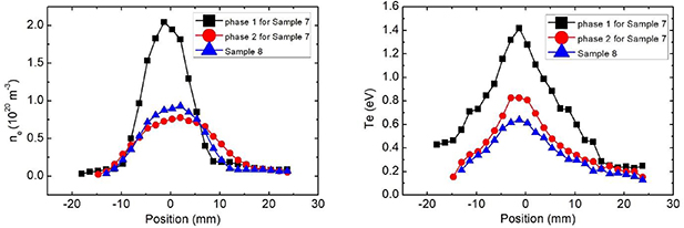
Figure 2. Plasma parameters during plasma exposure tests; (a) the distributions of electron density ne for samples 7 and 8; (b) the distributions of electron temperature Te for samples 7 and 8.
Download figure:
Standard image High-resolution imageTable 2. The experimental conditions of the plasma exposure tests for samples 7 and 8.
| Sample No. | Te (eV) | ne (×1020 m−3) | Tsurface (°C) | Tinterlayer (°C) | Additional conditions | Total exposure time (s) |
|---|---|---|---|---|---|---|
| 7a | 0.83 | 0.78 | 650 | 622 | Phase 1 with the high parameters for 15 s at the beginning (figure 2) | 215 |
| 8 | 0.64 | 0.93 | 519 | 497 | 400 pulses with the transient heat flux of 160 MW m−2 simultaneously | 200 |
aTe, ne, Tsurface and Tinterlayer of sample 7 in the table are only for phase 2 during case 1.
For case 2, sample 8 was exposed into a plasma with the electron density peak of  1020 m−3 and the electron temperature peak of 0.64 eV for 200 s, as shown in figure 2 and table 2. Moreover, a transient heat load of 0.16 GW m−2 given by a pulsed plasma was superimposed onto the sample simultaneously, which was used to evaluate the effect of heat fatigue on the interlayer due to ELM-like events. The pulse was in a triangle shape with the rise time of 0.65 ms and the decay time of 0.6 ms at the frequency of 5 Hz. A total of 400 pulses were applied to this sample during this experiment. Under the conditions of case 2, the surface temperature was kept at 519 °C, while the steady-state temperature of the TiN interlayer was 497 °C, which is at the upper limit of the possible working temperature of the first wall for DEMO.
5. Material analysis and discussion
It is extremely important to check the fabricated sandwich-like structure, the quality of the interlayer, the mechanics of the broken sample and the evolution of the W surface by material analysis. All of the eight samples were analyzed in this work. The microstructures of the samples were investigated by a scanning electron microscope (SEM) equipped with energy dispersive x-ray spectrometry (EDX).
5.1. The sandwich-like structure and the interlayer
The sandwich-like structure can be seen easily by SEM. Figure 3 shows the microstructure of the cross section of sample 5, which is typical for all of the samples. The sandwich-like structure, including CLF-1, CVD-W and the TiN interlayer, is shown clearly in figures 3(a), (b) and (c), where figures 3(b) and 3(c) give the details of the area B in figure 3(a) and the area C in figure 3(b), respectively. The thickness of the TiN interlayer is 0.96 µm in figure 3(c), while the distributions of different elements, including Ti and N, can be seen in figure 3(d), which indicates the apparent TiN interlayer between Fe and W. To deposit TiN well onto the CLF-1 substrate with good adhesion, the CLF-1 surface must have a certain roughness level. Therefore, a roughness level of about 1 µm is applied to the CLF-1 surface by polishing before the TiN coating fabrication, as shown in figure 3(c).
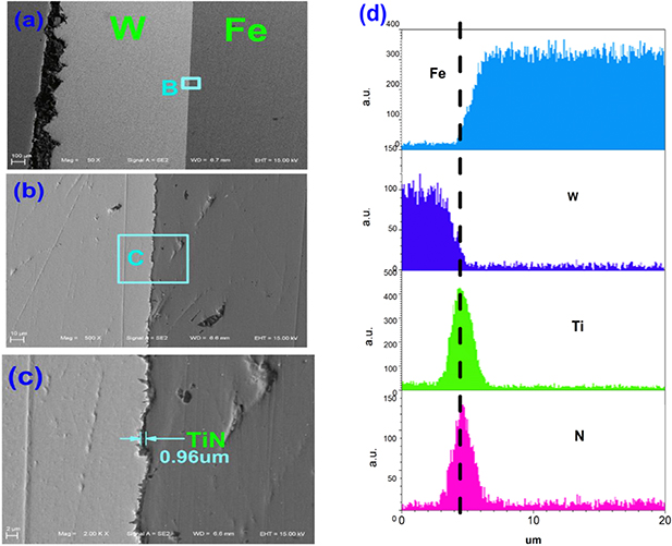
Figure 3. The sandwich-like structure and the element distributions in sample 5; (a) the microstructure of the cross section of sample 5; (b) the microstructure of the area B in (a); (c) the microstructure of the area C in (b); (d) the distributions of different elements in sample 5.
Download figure:
Standard image High-resolution image5.2. Mechanics of the broken sample
As shown in table 1, samples 1–5 delaminated during the wire-electrode cutting for preparation of the samples for testing and material analysis. By checking the microstructures of these samples by SEM and mapping the element distributions by EDX, the results show that all of these five samples were broken near the CLF-1 side. It is found that the fracture surface of the sandwich-like structure is always located in the CLF-1 material close to the interlayer or partially in the TiN layer near the CLF-1 substrate. A typical result of material analysis by EDX can be seen in figure 4, which shows the mapping of different elements on the fracture surface of the W side of sample 3. In figure 4(a), the species and percentages in area for different elements are given in the legend. Table 3 shows the weight and atomic percentages of different elements on this surface. Oxygen appears since the sample was analyzed days after being broken, and as a result, some particles on the surface were oxidized. From figure 3(a) and table 3, there is a lot of Fe, Ti and N on the surface but a lot less W, although this surface is on the W side of sample 3, which clearly implies that sample 3 was broken near the CLF-1 side. An unexpected phenomenon is that a large amount of fluorine (F) appears on the fracture surface. And F is always distributed in the same zone with Fe, different from the distributions of Ti, N and W. This fact can also be seen obviously from the mapping of different elements on the cross section of sample 6 in figure 7 later in this section. The F is introduced only by WF6 during the CVD of W, which indicates that the F penetrates into CLF-1 during the fabrication of CVD-W. Since TiN is a good barrier for tritium and other hydrogenic particles, as described in section 2.2, it would also be difficult for F to pass through TiN and then penetrate into the CLF-1 substrate. A reasonable explanation is that there are some defects in the TiN interlayer, and thus F penetrates into the substrate. The defect of the interlayer and the F penetration into CLF-1 cause the sample to break easily. As a comparison, the mapping of element distributions on the fracture surface of sample 7 is also checked. Sample 7 was not broken during cutting, the thermal cycling test and the plasma exposure test, but it was forced apart for material analysis after the exposure test. The percentages of different elements on the fracture surface of the CLF-1 side of sample 7 are presented in table 4. The results show that there is no F at all on the fracture surface. Since a large amount of Fe exists on this surface and F is usually distributed in the same zone as Fe, the data in table 4 provide evidence that no F penetrates and diffuses in the CLF-1 substrate of sample 7. Moreover, the material analysis is performed immediately after the sample is broken; as a result, no oxygen can be found on the fracture surface.
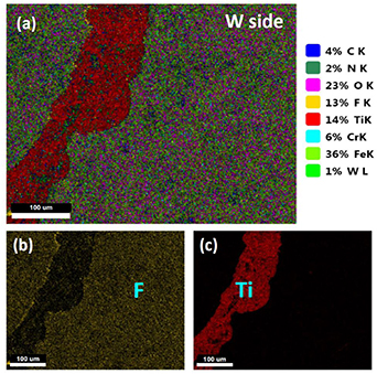
Figure 4. The mapping of different elements on the fracture surface of the W side of sample 3; (a) the distributions of all different elements on the fracture surface; (b) the distribution of F on the fracture surface; (c) the distribution of Ti on the fracture surface.
Download figure:
Standard image High-resolution imageTable 3. The percentages of different elements on the fracture surface of the W side of sample 3.
| Element | Weight % | Atomic % |
|---|---|---|
| C | 11.2 | 22.4 |
| N | 0.56 | 0.96 |
| O | 27.59 | 41.43 |
| F | 11.2 | 14.16 |
| Ti | 7.27 | 3.64 |
| Cr | 3.31 | 1.53 |
| Fe | 36.07 | 15.51 |
| W | 2.8 | 0.37 |
| Total | 100.00 |
Table 4. The percentages of different elements on the fracture surface of the CLF-1 side of sample 7.
| Element | Weight % | Atomic % |
|---|---|---|
| C | 3.87 | 13.87 |
| N | 6.93 | 21.30 |
| Ti | 19.46 | 17.48 |
| Cr | 5.12 | 4.24 |
| Fe | 52.17 | 40.19 |
| W | 12.44 | 2.91 |
| Total | 100.00 |
The mechanics of the broken sample and the defects of the TiN interlayer can be further analyzed by material analysis of sample 5. Figure 5 shows photographs of the fracture surface of the W side of sample 5. The TiN interlayer is displayed distinctly, and it covers the CVD-W in general. By mapping the element distributions with EDX, it is easy to identify the bright zones as the W material, as shown in figure 5. It implies that there are a lot of defects in the TiN interlayer where CVD-W was deposited and F penetrated during the CVD of W.
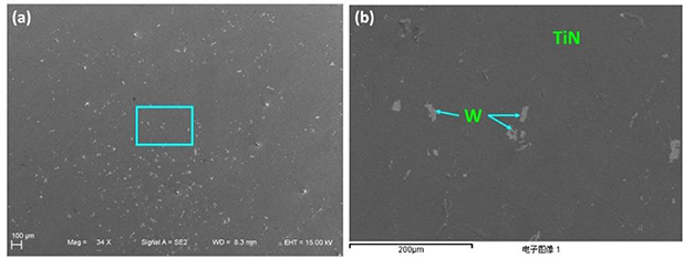
Figure 5. The views of the fracture surface of the W side of sample 5; (a) an overview of the fracture surface; (b) the details of the region in the blue box in (a).
Download figure:
Standard image High-resolution imageSample 6 was kept intact during cutting and the thermal cycling test and then broken accidentally before material analysis, which is a little different from samples 1–5. It seems that sample 6 has better bonding properties than samples 1–5. When checking the element distributions on the fracture surface of the W side of sample 6 by mapping with EDX, it is hard to find F within a random small zone, as shown in figure 6(a). But F can be identified when a wider area in the scale of a few square millimeters is checked. It implies that there are some defects in the TiN layer and the number of defects may be considerably fewer than those in samples 1–5. Then, the W side of sample 6 was cut in the region containing F, as shown in figure 6(b), to check the cross section of this specimen and understand the F behavior during the penetration and diffusion. The microstructures and the element distributions of this cross section are presented in figure 7. The CLF-1, the TiN interlayer and CVD-W can be seen clearly in figures 7(a), (b), (c) and (d). The results also show that F is distributed in the same region as Fe, which is consistent with the mapping photographs of the fracture surfaces of other samples. Moreover, the defect of the TiN layer is recognized in the blue circle in figure 7(g), and the patterns of the TiN interlayer and CVD-W in figures 7(g) and (h) are consistent with the results in figure 5. On the other hand, the F penetrates easily and diffuses uniformly into the CLF-1 substrate, which is evidence of the importance of a tritium barrier for the first wall of DEMO. Additionally, it is also verified that the sample was broken in the CLF-1 substrate close to the TiN interlayer according to the element distributions of Fe, Ti, N and W in figure 6 and the microstructures of the cross section in figure 7.
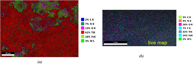
Figure 6. The element mapping on the fracture surface of the W side of sample 6: (a) mapping on a random small zone; (b) mapping on a wider zone.
Download figure:
Standard image High-resolution image
Figure 7. The microstructures and element distributions of the cross section of sample 6 within the region in figure 6(b): (a) an overview of the cross section; (b) the details of the cross section in the area B in (a); (c) the details of the cross section in the area C in (b); mapping of the area D; (e) the distribution of F in the area D; (f) the distribution of Fe in the area D; (g) the distribution of Ti in the area D; (h) the distribution of W in the area D.
Download figure:
Standard image High-resolution image5.3. Post-mortem analysis after plasma exposure
After the thermal cycling test at the temperature of up to 700 °C, samples 7 and 8 were exposed to hydrogen plasmas under the conditions in figure 2 and table 2. The surface temperature of sample 7 reached 1350 °C in phase 1 and then was kept at 650 °C in phase 2. During phase 2, the temperature at the TiN interlayer was 622 °C, which was a little bit higher than the upper limit of the working temperature of 300 °C–500 °C for the first wall of DEMO [1, 9, 11–14]. The temperature of the interlayer is the critical parameter for this plasma exposure test since it is important for evaluating the bonding property and the feasibility of the sandwich-like structure, while the behaviorof CVD-W under plasmas and heat loads has been investigated previously [2, 3]. For sample 8, it was exposed to a steady-state plasma as well as a pulsed plasma, which was used to simulate the heat fatigue due to ELMs. The temperature of the interlayer of sample 8 was set at 497 °C, right at the upper limit of the working temperature of the first wall. After the plasma exposure tests, the structural integrity of samples 7 and 8 still appeared good from visual inspection. The cross sections of these two samples were analyzed with SEM and are shown in figure 8. There is no obvious change seen at the interlayer, and no detachment or crack can be found in the structures of the samples, which implies that the bonding property of the interlayer is good enough under the working conditions for the first wall of DEMO. These encouraging preliminary test results support further examination of TiN as a potential interlayer material for W on RAFM steel as a first-wall material. For instance, improvement of the interlayer quality and the tritium permeation test may be required in the future.

Figure 8. The microstructures of the cross sections of samples 7 and 8 after the thermal cycling test and plasma exposure test: (a) the cross section of sample 8; (b) the cross section of sample 7.
Download figure:
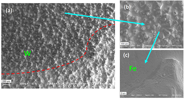
Standard image High-resolution imageAfter plasma exposure, the top W surface of sample 7 shows clear surface evolution. The surface roughness changes since the surface temperature is higher than the recrystallization temperature (RCT) of W due to overheating in phase 1. As a result, the grain growth can be seen clearly in figure 9(a), in which the red dashed line marks the boundary of the region with overheating. There are some particles deposited on the region without overheating, which is shown in figure 9(b). By mapping with EDX, it can be identified that the deposited particles are Fe due to the physical sputtering, and the details of the deposition are given in figure 9(c). For sample 8, there is no obvious morphological change except for some localized grain growth due to the overheating with the transient heat load of 0.16GW m−2 by pulsed plasmas. But there is no deposition of Fe at all since the ion temperature equal to the electron temperature in case 2 is much lower than that in phase 1 of case 1. More discussion on the CVD-W surface evolution is out of the scope of this work.
Figure 9. The microstructures of the top CVD-W surface of sample 7 after the plasma exposure: (a) the material evolution of the W surface; (b) the details of the region with deposition; (c) the details of the deposition zone.
Download figure:
Standard image High-resolution image
6. Summary and future plan
The new conceptual first wall structure with a TiN interlayer has been designed, fabricated and tested. The interlayer is used to control the tritium accumulation and bond the PFM CVD-W and the RAFM substrate. A thermal cycle test, plasma exposure test and material analysis have been implemented. The experimental results show that the TiN interlayer has sufficient adhesion as an interlayer between CVD-W and CLF-1 so far. The results of material analysis show that the quality of the TiN coating layer is critical for the adhesion and tritium prevention. With defects of the TiN interlayer, F penetrated into CLF-1 during the CVD-W fabrication and, as a result, the sandwich-like structure was broken near the CLF-1 side. The defects of the TiN interlayer could potentially be suppressed with a thicker TiN layer or a lower roughness value of the CLF-1 substrate before the TiN coating. Preliminary results indicate that the design and fabrication of the conceptual first wall are feasible. Further investigations, including the improvement of the interlayer quality, the maximum shear stress test and the tritium permeation test, are necessary in the future.
Acknowledgments
This work is supported by the International Collaboration Project of the Department of Science and Technology in Sichuan: No. 2016HH0006. DIFFER is part of the institutes organization of NWO. This work has been carried out within the framework of the EUROfusion Consortium and has received funding from the Euratom research and training programme 2014-2018 and 2019–2020 under Grant Agreement No. 633053. The views and opinions expressed herein do not necessarily reflect those of the European Commission. We acknowledge the support of the Magnum-PSI Facility Team at DIFFER. The Magnum-PSI facility at DIFFER has been funded by the Netherlands Organization for Scientific Research (NWO) and EURATOM.