
Abstract
Objective. Methods for the detection of neural signals involve a compromise between invasiveness, spatiotemporal resolution, and the number of neurons or brain regions recorded. Electrode-based probes provide excellent response but usually require transcranial wiring and capture activity from limited neuronal populations. Noninvasive methods such as electroencephalography and magnetoencephalography offer fast readouts of field potentials or biomagnetic signals, respectively, but have spatial constraints that prohibit recording from single neurons. A cell-sized device that enhances neurogenic magnetic fields can be used as an in situ sensor for magnetic-based modalities and increase the ability to detect diverse signals across multiple brain regions. Approach. We designed and modeled a device capable of forming a tight electromagnetic junction with single neurons, thereby transducing changes in cellular potential to magnetic field perturbations by driving current through a nanofabricated inductor element. Main results. We present detailed quantification of the device performance using realistic finite element simulations with signals and geometries acquired from patch-clamped neurons in vitro and demonstrate the capability of the device to produce magnetic signals readable via existing modalities. We compare the magnetic output of the device to intrinsic neuronal magnetic fields (NMFs) and show that the transduced magnetic field intensity from a single neuron is more than three-fold higher at its peak (1.62 nT vs 0.51 nT). Importantly, we report on a large spatial enhancement of the transduced magnetic field output within a typical voxel (40 × 40 × 10 µm) over 250 times higher than the intrinsic NMF strength (0.64 nT vs 2.5 pT). We use this framework to perform optimizations of device performance based on nanofabrication constraints and material choices. Significance. Our quantifications institute a foundation for synthesizing and applying electromagnetic sensors for detecting brain activity and can serve as a general method for quantifying recording devices at the single cell level.
Export citation and abstract BibTeX RIS

Original content from this work may be used under the terms of the Creative Commons Attribution 4.0 license. Any further distribution of this work must maintain attribution to the author(s) and the title of the work, journal citation and DOI.
1. Introduction
From basic neuroscience to neurology, the ability to decode neural activity with minimized invasiveness and little compromise to spatiotemporal precision has long been the goal of experimenters and clinicians [1–3]. Implantable electrodes are the most typical brain interface allowing for single-neuron electrophysiological readouts, but they are invasive, requiring long-term transcranial connections with readouts limited by the size of the device [4, 5]. Techniques such as electroencephalography (EEG) and magnetoencephalography (MEG) offer an entirely noninvasive alternative, enabling remote recording of electrophysiological signals at the scalp, but do not provide readouts at single-neuron resolution [6, 7]. Due to amplitude attenuation and spatial distortion of local field potentials (LFPs) through neural tissue and the skull, EEG provides a measure of LFPs originating from large aggregates of neurons within the cortex, with spatially shifted readouts and signal amplitude attenuation proportional to the square of the distance from its source [6, 8]. In contrast, magnetic fields in the brain are only minutely attenuated or distorted, and can therefore be detected with higher spatial precision and improved localization using sensitive magnetometers [7, 9]. MEG readouts still arise from large populations of neurons firing synchronously, and likely reflect activity developing from neural currents within shallow areas of cortical sulci that are properly aligned to the magnetic detection devices [7]. Bridging the gap between noninvasive neuroimaging and single-neuron invasive electrophysiology can potentially open the door to a new milieu of brain readouts.
Quantifications of intrinsic neuronal magnetic fields (NMFs) arising from the excitation of single neurons, subcellular compartments, and multicellular neuronal populations, were carried out computationally by several groups and can determine possibilities for NMF detection without the need for invasive transcranial wiring at the time of recording [10–13]. These studies informed the interpretation of MEG recordings [7, 14] and catalyzed the design of specialized pulse sequences, phantom measurements and distilled preparations for magnetic resonance imaging (MRI) in attempts to detect NMFs volumetrically [15–19]. To date, real-time detection of NMFs by MEG at native in vivo scenarios, in the presence of motion artifacts, and blood flow related electromagnetic disturbances [7, 20, 21] requires severe averaging of consecutive trials evoking coordinated activity of many neurons, and has not yet been demonstrated convincingly by volumetric modalities [15, 22]. This points to a requirement for in situ agents similar to emerging contrast agents for direct neuroimaging of calcium [23–25] and neurotransmitters [26–29], that could similarly facilitate direct detection of NMFs across the brain.
Here, we present an approach for enhancing magnetic fields in response to intrinsic electrophysiological events using nanofabricated planar inductors that are interfaced with single neurons and designed to act as agents that transduce neural activity into readable magnetic signals. The interface relies on high electromagnetic coupling promoted by nanofabricated protrusions previously shown to generate a tight cleft between cells and electrodes [30, 31] and to yield increased electrical response to neural activity [32–34]. Using a realistic finite element framework with nanometer scale resolution, we quantify the ionic fluctuations induced in the neuron coupled to the device by using patch clamp recordings of mammalian cortical neurons as signal input. We quantify the voltage drop developing between the interface pad at the center of the inductor and an extended reference pad facing the extracellular solution, and then determine the amplitude and spatiotemporal characteristics of the magnetic field response resulting from membrane potential changes that drive current through the device. We use our results to perform optimizations of the geometry of the device while conforming to nanofabrication constraints and reach an optimized design that is able to transduce electrophysiological signals to a magnetic field approximately 300 times greater in magnitude perpendicular to the plane of the inductor and cell culture surface than those produced intrinsically by individual neurons when averaged across a volume. Our approach could immediately enable sensitive detection of single-neuron activity in vitro and pave the way for potential future designs applied with modalities such as MEG and MRI.
2. Methods
2.1. Device fabrication
Devices were fabricated by electron beam lithography on glass or high resistivity silicon dies. A2/A4/A6 poly methyl-methacrylate (PMMA) 495 (Kayaku Advanced Materials Inc. MA, USA) was spin-coated on samples at 3000 RPM for 30 s and baked in a convection oven for 30 min. Direct write of inductor patterns was then performed by electron beam lithography (Elionix, Tokyo, Japan) followed by development of the resist using methyl isobutyl ketone/isopropyl alcohol (MIBK/IPA) (1:2). Ti/Au (1:10) was deposited by electron beam deposition followed by PMMA lift off in ultrasonicated acetone (5 min) at room temperature. Silicon oxide insulating layer was deposited by plasma-enhanced chemical vapor deposition. An additional nanolithography step was performed to define the ground pad and protruding pillars at the interface pad, followed by buffered oxide etching through the silicon oxide layer. Au protrusions were grown by electron beam deposition PMMA was lift off. Samples were then cleaned in IPA and cultured with neurons as described below to demonstrate biocompatibility (figure 1(b)). The device optimization described below uses a device geometry successfully fabricated in this way as a starting point.

Figure 1. Model of single-neuron magnetic fields enhanced by nanofabricated coils. (A) A patch clamped primary cortical rat neuron microinjected with fluorescently labeled biocytin, traced digitally for use in the model. Scale bar: 30 µm. (B) Neuron growing on top of a nanofabricated coil (green: calcein AM, grayscale: differential interference contrast). Scale bar: 30 µm. Inset: a neurite interfaced with a mushroom-shaped cell-adhesion protrusion nanofabricated at the interface pad at the center of the coil. (Scale bar: 30 µm). (C), (D) top (XY) views of the model of the naïve (C) and nanocoil-enhanced (D) neuron. Surface color plot, electrical field strength. Slice color plot, magnetic field strength. Inset arrow plot, magnetic flux. Dashed colored lines correspond to (E), (F), magnetic field magnitude (nT) across the X dimension. Colored bands: corresponding standard deviation.
Download figure:
Standard image High-resolution image2.2. In vitro cell culture
Primary cortical neurons were cultured on substrates following previously described protocols [35]. Glass or device surface was sterilized for 15 min in ethanol, then a portion of each sample was prepared with a 50 µl droplet of sterile filtered aqueous 0.1 mg ml−1 poly-d-lysine (Gibco A38904-01) and 4 µg ml−1 laminin (Gibco 23017-015). Coverslips sat for 60 min in incubator conditions (37 °C, 5% CO2, 95% humidity), were rinsed three times with 1x phosphate buffered saline (PBS), then stored at 4 °C overnight. Primary cortical rat neurons (Gibco A10840-01, Lot 2111507) were thawed from dry ice (−80 °C) for 2 min without agitation in a 37 °C water bath. A 15 ml conical tube and 1 ml micropipette tip were rinsed with plating media (Neurobasal Plus, Gibco A3582901; 10% FBS Gibco 10437010; 1× GlutaMAX, Gibco 35050-061), the tip was used to transfer the cell suspension from the cryotube to the conical tube, 1 ml of plating media was added dropwise for a final concentration of 500 000 cells ml−1, and 300 µl of cell suspension (150 000 cells) were plated onto each sample. The cultures sat in incubator conditions for 4 h before plating media was removed and 3 ml maintenance media (Neurobasal Plus, 1× B27 Plus Gibco A3582801, 1× GlutaMAX) were added to each 35 mm well. 1.5 ml media changes were performed every 3–4 days (Mondays and Fridays). Cells on devices were stained with 10 μg ml−1 calcein AM (Invitrogen C3099) in media for 20 min at 37 °C followed by a 20 min rest in stain-free media at 37 °C before imaging for visualization (figure 1(b)).
2.3. Patch clamp recordings
At 24 days in vitro (DIV) samples on glass coverslips were removed from maintenance media and placed in extracellular solution (ECS; in mM, NaCl 145, KCl 5, MgCl2 1, CaCl2 1, HEPES 5, Glucose 5, Sucrose 20, D-serine 0.01, adjusted to pH 7.4 with NaOH and 315 mOsm with sucrose). All solutions were prepared with culture grade H2O (Corning 25-055-CVC). Filamented glass pipettes (8250 Glass, A-M Systems 596800 were pulled on a P-97 pipette puller (Sutter Instruments, Novato, CA) to create 5–10 MΩ micropipettes. Pipettes were backfilled with intracellular solution (ICS; in mM, KCl 120, HEPES 10, ATP.Na 5, GTP.Na 0.2, EGTA 10, adjusted to pH 7.2 with KOH), mounted on a Sutter IPA Headstage with a Ag/AgCl coated wire driven by a Sutter Quad micromanipulator and connected to a Sutter Double IPA patch clamp amplifier for recording via SutterPatch (v. 2.04, Sutter Instruments, Novato, CA) within Igor Pro software (v. 8.04, WaveMetrics, Portland, OR) in current clamp configuration. For staining experiments, ICS included 20 µM of biocytin (Sigma B4261). Upon breaking through the plasma membrane, biocytin diffused into the cell, allowing imaging of the neuron processes for morphological registration used for simulations (figure 1(a)). Electrophysiology experiments were performed using Olympus BX51WIF microscope (Olympus America Inc., Waltham, MA) and ORCA-Flash4.0 V3 C13440 Digital sCMOS camera (Hamamatsu, Japan) for optical acquisition during biocytin injection.
2.4. Model neuron
Biocytin-injected neuron morphology (figure 1(a)) was traced to create a vector representation, which was imported into COMSOL multiphysics simulation environment (COMSOL Inc., Stockholm, Sweden). Geometry was extruded to a height of 1.1 µm (figure 1(c)). The membrane was modeled with exterior surface area 1450 μm2, volume 14.39 μm3, relative permeability  = 1, relative permittivity μ = 1, electrical conductivity σ = 1 × 10⁻¹³ S m−1, surrounding the intracellular environment, surface area 1431.1 μm2, volume 463.77 μm3, which was modeled using the electrical properties of cerebrospinal fluid, = 1.09 × 10², μ = 1, σ = 2 S m−1. Representative action potential (AP) data was extracted from voltage traces of current clamp recordings (figure 3(a), sampling frequency = 6103.5 Hz, total recording time 23:51.768) and used as input for an electronic circuit simulation software (LTSPICE, Analog Devices, Norwood, MA). The cell-device interface was simulated as a 100 MΩ resistor in parallel with a 15 pF capacitor. The current was measured across this interface and downsampled to 20 key values, which were applied as inputs in COMSOL on one face of the neuron in a parametric sweep stationary study for simulations of magnetic flux density and field strength during APs to compare the response of the naïve model neuron to that of the modeled cell-device interface (figure 3(c)).
2.5. Device modeling and optimization
Simulations and optimizations of device response and device-neuron interface were performed in COMSOL. Patterns used for nanofabrication were imported and extruded along the z-axis. The electrical properties of the device were set to those of gold, = 1, μ = 1, σ = 1 × 10⁶ S m−1. This gold layer thickness was tested at 100, 500, 1000, and 1500 nm. Lateral width of the inductor conducting turns was tested at 540, 730, 940, and 1020 nm using a constant center-to-center turn distance of 1478 nm. Given a constant outer diameter (75 µm edge-to-edge, 80 µm corner-to-corner), turn width (1.0 µm edge-to-edge, 1.1 µm corner-to-corner), and turn spacing (0.46 µm edge-to-edge, 0.50 µm corner-to-corner), the number of turns was varied and represented as the percentage of the total diameter left open at its core. The open core percentage was tested at 10.9% (23 turns), 22.6% (20 turns), 34.4% (17 turns), 46.2% (14 turns), 57.9% (11 turns), and 65.8% (9 turns). All device geometries were tested using representative current input of 1 nA through the interface pad at the center of the inductor. The optimized device geometry was used to model the magnetic response when coupled with the model neuron. The effects of various substrates were tested using the same input current by varying the material properties of a 25 × 50 × 100 µm block beneath the device between glass, = 4.7, μ = 1, σ = 2.3 × 10⁻²¹ S m−1; polyimide, = 3.8 [36], μ = 1, σ = 6.7 × 10⁻¹⁸ S m−1; parylene, = 3.1 [36], μ = 1, σ = 1.136 × 10⁻¹⁵ S m−1; and silicon of various conductivities, = 11.68, μ = 1, σ = (0.01, 0.1, 1, 10, 100, 1000, 10 000, 100 000) S m−1 (0.001 Ω cm to 10 000 Ω cm). Magnetic field values were extracted from the model either linearly across a 120 µm × 1 µm × 1 µm region of interest (ROI) centered at various Y coordinates on the Z = 0 plane, or volumetrically within a 40 µm × 40 µm × 10 µm ROI centered at the cell-device interface pad, in the X, Y, and Z axes. For linear scans, the mean and standard deviation of the absolute magnetic field magnitude were taken along the Y/Z axes within the ROI. Separately, absolute magnetic field amplitude was taken along a 20 µm, Y-aligned line on the Z = 0 plane, centered on the neurite 2 µm away from the input port (supplementary figure 1) to compare the magnetic field amplitude of the neuron with and without the presence of the device. Volumetric values averaged the Z component of the magnetic field across the ROI. For optimizations of device geometry and substrate testing, the Z component of the magnetic field output was extracted at an XZ slice of the model arena at the Y coordinate corresponding to the center of the coil and used to compare the output of each model instance.
3. Results
3.1. Enhancement of intrinsic NMFs by nanofabricated coils
In order to explore the feasibility of enhancing intrinsic NMFs by nanofabricated coils (nanocoils) interfaced with single neurons, we generated a realistic finite element model of a cell coupled to device and quantified the magnetic field response to current injected into the cell (figure 1). The model uses morphology extracted from primary cortical neurons injected with fluorescently labeled biocytin via patch micropipette electrodes (figure 1(A) and supplementary figure 2). Neurons grew on glass coverslips or nanofabricated devices for up to 24 DIV (figure 1(B)). We input a series of key current values into the model, extracted and calculated from a patch clamp recording of cells on coverslips (figure 3(c)), with a peak of 1.7 nA intracellular current in the model cell (figure 1(C)), resulting in intracellular electric fields of up to 1.2 mV µm−1 and extracellular electric fields up to 30 µV mm−1 within 2 µm of the neurite membrane (supplementary figure 2(C)), and the transmembrane electric field gradient reaching 11 mV nm−1 as previously seen both in vitro and in vivo [37]. The absolute amplitude of the magnetic field observed near the neuron in response to current injection reached values of up to 0.51 nT and decays to <1% of peak signal within an average of 30 µm of the neuron, similarly to previous models of single-cell NMFs [11, 12]. We next quantified the magnetic field amplitude at a volume surrounding the same 1.7 nA current-injected neuron coupled to a nanocoil (figure 1(D)). The neuronal membrane was coupled to the interface pad in the middle of the nanocoil (figure 1(D), a). The magnetic field amplitude at various line scans across the X axis (figure 1(D), (a–e)) reached values of up to 1.6 nT and decayed to <1% of peak within an average of 19 µm from the outer turns of the nanocoil. In the case of line a (figure 1(D)), which crosses the interface pad, the magnetic field decayed to <1% of peak an average of 46 µm from the interface pad. We quantified the spatial distribution of NMFs in the naïve neuron not coupled to the device within a 1 µm by 1 µm cross sectional area around various line scans across the X axis and found that across three representative somatic and neurite compartments (figures 1(c), (a–c) and (E)) the full widths at half maximum (FWHM) of magnetic field magnitude were (a) 2.7 µm, (b, soma) 7.9 µm, and (c) 7.1 µm. In contrast, the spatial distribution of magnetic fields near a neuron coupled to a device across five representative regions (figures 1(D), (a–e) and (F)) was spatially enhanced with FWHM of (a) 67 µm, (b) 72 µm, (c) 62 µm, (d) 46 µm, and (e, ground pad) 16 µm. The magnetic field amplitude of the neuron itself was not significantly changed when coupled to the device, reaching levels of up to 0.60 nT in the neurite of the naïve neuron and 0.25 nT in the neurite of the neuron enhanced by the device, measured 2 µm from the neurite input port (supplementary figure 1), within the bounds of minimal magnetic interference. In summary, the magnetic field amplitude output by the device driven by cellular potentials is more than three times greater at its peak (1.6 nT vs 0.51 nT) across a ten times wider lateral distance (72 µm from the device vs 7.1 µm from the neurite) than the intrinsic NMF. Looking at a 40 × 40 × 10 µm voxel, discussed below, this results in a 250-fold spatial enhancement (640 pT vs 2.5 pT, see figure 3).
3.2. Analysis of device geometry
Based on the initial geometry used to quantify the magnetic response of a neuron-device interface, we performed optimizations of design features to explore maximal transduction while obeying nanofabrication limitations (figure 2). Three main parameters tested included the vertical thickness of the device metallization layer (figures 2(A)–(C)), the lateral width of the nanocoil turns (figures 2(D)–(F)), and the number of turns as represented by the open core percentage (figures 2(G)–(I)). For each parameter value, we compared the mean z-axis component of the magnetic flux density (Bz ) within a ROI across a XZ slice over the center of the device, spanning 50 µm along the x axis, and 12.5 µm along the z axis. The bottom of the slice was aligned to z = 0, coplanar with the bottom plane of the device (figures 2(A), (B), (D), (E), (G) and (H), bottom panel).
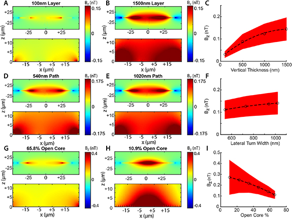
Figure 2. Optimizations of device geometry. Magnetic transduction was optimized based on design parameters including the thickness of the device metallization layer (A)–(C), turn width (D)–(F), and the ratio between the inner and outer diameters of the nanocoil (G)–(I). (A), (B); (D), (E); (G), (H) XZ section views of magnetic flux density in Z for models on the extremes of each optimization. Top, full view of model geometry. Bottom, zoomed view of the region of interest (ROI) used to calculate induced field strength. (C), (F), (I) scatter plots of each pixel in ROI views. Large circle, mean. Red band: standard deviation. Black dashed line: polynomial fit of means.
Download figure:
Standard image High-resolution imageWe used the initial geometry (turn width of 334 nm, core 57.9%) and varied the vertical gold layer thickness by extruding the device to values of 100, 500, 1000, and 1500 nm (figures 2(A)–(C)), yielding average field strength Bz = 0.030 ± 0.013 nT, 0.086 ± 0.033 nT, 0.12 ± 0.04 nT, and 0.13 ± 0.05 nT, respectively. Proceeding with a 500 nm thick gold layer, we next quantified the effect of nanocoil turn width on the average magnetic field strength Bz at the device surface (figures 2(D)–(F)). Turn width was set to 540, 730, 940, and 1020 nm, yielding average field strength Bz = 0.11 ± 0.04, 0.13 ± 0.04, 0.14 ± 0.04 and 0.14 ± 0.05 nT, respectively (figure 2(F)). Predictably, the widest path induced the strongest magnetic field strength. We turned to testing the effect of the total number of turns, while maintaining a constant outer diameter (80 µm), neural interface pad diameter (when allowed by the core size, 14 µm), coil thickness (500 nm), turn width (1020 nm), and turn spacing (1478 nm) (figures 2(G)–(I)). We represent this as the ratio of the inner to the outer diameter, or the percentage of the outer diameter that makes up the open core of the nanocoil. We tested values 10.9% (23 turns), 22.6% (20 turns), 34.4% (17 turns), 46.2% (14 turns), 57.9% (11 turns), and 65.8% (9 turns), which yielded mean Bz = 0.27 ± 0.16, 0.25 ± 0.12, 0.22 ± 0.08, 0.18 ± 0.06, 0.14 ± 0.04 and 0.11 ± 0.03 nT, respectively (figure 2(I)). Predictably, smaller cores produced higher peak magnetic field strength perpendicular to the plane of the coil (peak Bz = 1.1, 0.85, 0.79, 0.73, 0.67 and 0.52) while the minimum field strength observed at the periphery of the ROI remained stable across different conditions (min Bz = 0.057, 0.058, 0.061, 0.064, 0.060, and 0.061 nT).
3.3. Single neuron activity on optimized device
We analyzed the magnetic field developing at the neuron-device interface during a typical AP selected from a series of spontaneously occurring spikes recorded via patch clamp (figure 3(a)). Modeled magnetic field was averaged across a 40 × 40×10 µm voxel extending 20 µm to each side of the center of the coil, and 5 µm above and below the coil (figure 3(B)). The same voxel dimensions were used to average the modeled magnetic output of the naïve neuron. Absolute AP amplitude was 72 mV, and the after-hyperpolarization voltage was −8.2 mV (figure 3(c)). The AP voltage trace was run through the equivalent circuit of a neuron to derive the current trace (figure 3(c), purple). The current peaked at 1.7 nA during depolarization and had a minimum of −0.80 nA during the after-hyperpolarization stage. The magnetic field perpendicular to the plane of the neuron and nanocoil peaked at 2.5 pT for the naïve neuron, and at 640 pT for the neuron enhanced by the device. The magnetic field perpendicular to the plane of the geometry induced by the downswing current was −1.2 pT for the naïve neuron and −300 pT for the enhanced neuron. The overall spatial enhancement of the transduced magnetic field output within a voxel was 250-fold higher than the intrinsic NMF.

Figure 3. Modelling the response to a recorded action potential. (A) 500 ms trace of a spike train recorded via patch clamp of primary cortical neuron. Window used in model is highlighted by dashed box. (B) Axes planes illustrating the magnetic field induced in the coil at six points (a)–(f) along the action potential, corresponding to marked points on (C) and (D). (C) Comparison of voltage and current traces of action potential. Left axis, solid black line: change in membrane potential from resting potential (mV). Right axis, data points: 20 current values calculated from voltage trace. Purple dashed line, Gaussian fit of current data (nA). (D) Comparison of magnetic field between device-enhanced and naïve neurons (square and triangle markers, respectively). Left axis, solid black lines: Gaussian fit of magnetic field strength in nT. Right axis, dashed red line: Gaussian fit of magnetic field strength in pT, to highlight the scale of the naïve neuron's response.
Download figure:
Standard image High-resolution image3.4. Substrate testing
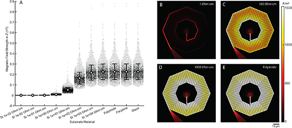
To evaluate performance on substrates compatible with nanolithography that are commonly used for implantable devices, we quantified the magnetic transduction of nanocoils embedded on dielectric substrates including glass, parylene and polyimide, and on silicon with various levels of doping (figure 4). High resistivity silicon (1000 Ω cm and 10 000 Ω cm) and all dielectric substrates displayed strong induced magnetic fields (figure 4(A)) with average magnetic field strength of 0.23 ± 0.08 nT for dielectrics, 0.22 ± 0.07 nT for 10 000 Ω cm Si, and 0.22 ± 0.07 nT for 1000 Ω cm Si. Low resistivity silicon (0.001, 0.01, and 0.1 Ω cm) demonstrated predictable current shunting, and weak induced magnetic fields, with average field strength of 4.8 × 10⁻⁶ ± 3.8 × 10⁻⁴nT, 8.5 × 10⁻⁵ ± 2.1 × 10⁻⁴ nT, and 9.7 × 10⁻⁴ ± 7.1 × 10⁻⁴ nT, respectively). Silicon substrates with resistivities of 1, 10, and 100 showed an intermediate effect, with average field strength of 0.0080 ± 0.0048, 0.052 ± 0.022, and 0.16 ± 0.06 nT, respectively). Current density was largely in proportion to field strength, reaching maximal levels of 880 A m−2, 2400 A m−2, 2800 A m−2, and 2800 A m−2 for 1, 100, 1000 Ω cm Silicon and for Polyimide, respectively (figures 4(B)–(E)).
Figure 4. Quantification of magnetic transduction on common fabrication substrates. (A) Average magnetic field strength on polyimide, parylene, glass, and silicon substrates with a range of ion implantation doses, measured within XZ planes as in figure 2 (Error bars, standard deviation. Beeswarms, magnetic field strength at each pixel within measurement plane.). (B)–(E) XY views of the current density on 1 Ω cm (B), 100 Ω cm (C), and 1000 Ω cm (D) silicon, and polyimide (E).
Download figure:
Standard image High-resolution image
4. Discussion
Our model validates a new principle for amplifying neurogenic magnetic fields by interfacing single neurons with nanofabricated flat spiral coils. The junction formed between cell and device relies on tight electrical coupling at the interface pad and generates magnetic fields that are enhanced both spatially and in amplitude, compared with the driving NMF. We show that the predicted magnetic field magnitude in response to neural currents surrounding the device is more than three-fold higher in peak amplitude compared to intrinsic NMF, reaching 1.6 nT in the plane of the coil. Averaging the signal over a volume of 40 × 40 × 10 µm3 results in 640 pT compared with 2.5 pT for a naïve neuron and an overall spatial enhancement of the transduced magnetic field output of more than 250-fold. Our approach brings about immediate relevance to in vitro magnetometry but also has potential relevance to modalities such as MRI and MEG, whereby arrays of nanofabricated devices of sufficient density can modulate signal change in response to neuronal activation. Our approach could provide a way to overcome the theoretical limitations of spatial resolution and sensitivity of these modalities that thus far precluded detecting micrometer scale picoTesla events without transcranial wiring at the time of recording.
Effective coupling for remote electromagnetic detection depends on nanofabrication features that dictate impedance and inductance [38–40]. The geometric optimization delivered by our model provides recipes that can be applied on unique substrates for increased magnetic transduction, while adhering to the practical limitations of nanofabrication techniques. One unique avenue for application is nanofabrication of nanocoils on emerging nitrogen vacancy (NV) diamond substrates used for fluorescence-based micro-magnetometry [41, 42]. This technology enables highly sensitive magnetic detection of resolved 400 pT transient magnetic events resulting from APs in nerve preparations [43] and single-cell superparamagnetic nanoparticle internalization in vitro [44]. These studies could benefit from enhanced fields by arrays of nanocoils that can provide multiplexed single-neuron readouts of neuronal networks, and this modality is sensitive enough to capture the theoretical magnetic output of a single nanocoil device. More broadly, NV diamond magnetometry employs microwave resonance at the 2.87 GHz regime, inviting integration of capacitors into the nanocoil device for microwave resonance and high spatial resolution modulation of fluorescence by magnetic fields. Lithography of high aspect-ratio inductors offers reduced impedance and increased inductive coupling but can also present constraints due to possible structural collapse of device features [45–47]. In this study, we analyzed metallization layers ranging between 100 nm and 1.5 µm, and show a predictably high magnetic field of 0.13 nT produced at the highest thickness with a 1 nA current. We find that thickness of 500 nm with 1020 nm turn width, yielded a comparably strong magnetic field of 0.14 nT, with features that maintain 1:1 or smaller aspect ratio and are well within the capabilities of electron beam lithography and Au growth techniques. Other significant features include the interface pad at the core of the device that acts as a common electrode driving the magnetic field generation at the nanocoil. The size of the coil's open core impacts the size of the interface pad, turn density and overall magnetic field strength. A core with a diameter only 10.9% the diameter of the nanocoil was found to produce the highest peak magnetic field, (0.27 ± 0.16 nT) but with very high standard deviation across the 12.5 × 50 µm plane tested. A core of a 46.2%, allowed for a sufficiently large 14.4 µm interface pad, a low variability magnetic field of 0.18 ± 0.06 nT and overall optimal performance.
Our model mimics the generation of ionic currents during APs at sub-cellular neurite morphologies on a flat device in vitro. Currents propagating in neuronal compartments induce magnetic fields that rotate around the axis of neurite at specific orientations during synaptic events and aggregate to form a typical MEG signal measured outside of the brain [7, 9]. A flat spiral nanocoil interfaced with a neuron is predicted to generate magnetic fields rotating about the turns of the coil, aggregating to a large field spread over an area perpendicular to the plane of the substrate irrespective of the original NMF alignment to the detector. This offers a new repertoire of MEG measurements from untapped anatomical orientations and depths in vivo, assuming sufficiently dense multiple aligned coil arrays are implanted. We examined magnetic fields on commonly used implantable substrates including high resistivity silicon, glass, polyimide and parylene. We find no magnetic field loss on these substrates, leading to potential long-term implantation of nanocoils leveraging known chronic biocompatibility for these substrates. Flexible substrates are of particular importance and can facilitate MEG signal enhancements when implanted similarly to dense electrocardiogram devices that conform to anatomical features in the brain [48, 49]. Such an array would theoretically allow for measurement of single cell activity in vivo without the need for transcranial wiring. Moreover, previous MRI phantom measurements of a 30 µm wire demonstrate detectability of fields as low as 200 pT for a 2.5 × 2.5 × 6 mm voxel [50]. Given that our 80 µm device produces a 640 pT volumetric magnetic field, it is feasible that the field produced by a single device coupled with a firing neuron will be detectable via MRI. In conclusion, our quantifications institute a foundation for synthesizing minimally invasive electromagnetic sensors for detecting brain activity and can serve as a broad protocol for quantifying sensitivity at the single cell level.
Data availability statement
The data that support the findings of this study are available upon reasonable request from the authors.
Author contributions
A H, M G and J K P designed the research. J K P and M G performed the research. J K P, M G and Y G analyzed the data. A A, M D and A H fabricated the device, J K P performed cell imaging and patch clamp experiments. J K P and A H wrote the manuscript.
Conflict of interest
The authors declare no competing interests.
Funding
This work was supported by the National Institute of Neurological Disorders and Stroke and the Office of the Director's Common Fund at the National Institutes of Health (Grant DP2NS122605 to A H), the National Institute of Biomedical Imaging and Bioengineering (Grant K01EB027184 to A H) and the Wisconsin Alumni Research Foundation (WARF).