

Abstract
Objective. In many applications, multielectrode arrays employed as neural implants require a high density and a high number of electrodes to precisely record and stimulate the activity of the nervous system while preserving the overall size of the array. Approach. Here we present a multilayer and three-dimensional (3D) electrode array, together with its manufacturing method, enabling a higher electrode density and a more efficient signal transduction with the biological tissue. Main results. The 3D structure of the electrode array allows for a multilayer placement of the interconnects within a flexible substrate, it narrows the probe size per the same number of electrodes, and it maintains the electrode contacts at the same level within the tissue. In addition, it augments the electrode surface area, leading to a lower electrochemical impedance and a higher charge storage capacity. To characterize the recordings capabilities of the multilayer 3D electrodes, we measured visually evoked cortical potentials in mice and analysed the evolution of the peak prominences and latencies according to different light intensities and recording depths within the brain. The resulting signal-to-noise ratio is improved compared to flat electrodes. Finally, the 3D electrodes have been imaged inside a clarified mouse brain using a light-sheet microscope to visualize their integrity within the tissue. Significance. The multilayer 3D electrodes have proved to be a valid technology to ensure tissue proximity and higher recording/stimulating efficiencies while enabling higher electrode density and reducing the probe size.
Export citation and abstract BibTeX RIS
1. Introduction
Implantable multielectrode arrays (MEAs) have been widely used in neuroprosthetics as a means for signal transduction from and to the nervous system [1–4]. Microelectrodes can modulate neuronal activity and record spikes or local field potentials in their proximity [5, 6]. As a result of the scientific and technological progress in materials science and microengineering, the field of neuroprosthetics is steadily progressing towards more efficient devices, with improved neuroelectronic interfaces [7]. A generally desired characteristic of implantable MEAs is a high density of electrodes leading to a high-resolution prosthesis, and in some cases, ideally reaching the single neuron level [8, 9]. High-resolution prostheses can be useful in various applications, such as in artificial vision to replace degenerated photoreceptors with a retinal implant [10–12].
Micro- and nanofabrication technologies offer nowadays the opportunity to manufacture thin and flexible implants with electrode sites in the order of few microns in size [13, 14], meaning that is possible to obtain probes with a very high electrode density (up to about 1000 electrodes per mm−2). Nevertheless, a limitation associated with the increment of the electrode number and density is the increase in the number of traces connecting the implanted array to external electronic devices. In turn, this would increase the implant invasiveness by requiring a wider connecting cable. It is, therefore, necessary to reach a compromise between the size of the probe and number of electrodes. As an example, most epiretinal prostheses rely on a trans-scleral cable to connect the implanted electrode array to the extra-ocular electronic case [15]. A trans-scleral cable is recognized as a weak point because it may cause eye inflammation or leakage through the pars plana incision followed by hypotony [16]. To reduce the risk of such events, the trans-scleral cable must be limited in its width (in general less than 2 mm). In turn, this constraint imposes a limitation on the maximum number of electrodes that can be addressed [17].
In this perspective, multilayer fabrication allows for the placement of electrodes with their interconnects on different levels, thus allowing an increase in the electrode density while maintaining a reasonable implant size [18, 19]. An example of multilayer placement is visible in figure 1(a), where three electrodes can be placed on three different layers (bottom) instead of one (top), with a slight—and mostly irrelevant—increase in thickness, but an important reduction in width (see red arrows). Under this condition, a trilayer electrode array may on average duplicate the number of electrodes per unit area (figure 1(b)). Nevertheless, a common drawback when using multilayer probes is the increased and inconsistent distance between the electrodes and the overall surface of the implant (figure 1(c), flat), or in other words, the electrode-tissue distance. This separation is an important parameter to be minimized for an efficient implantable neuroprosthesis [5, 20–22]. In case of neural recordings, the closer the electrogenic cell is to the electrode, the higher is the probability of detecting and specifically identifying its neural activity. In the case of neuronal stimulation, the reduction of the electrode-tissue distance improves the spatial selectivity [23, 24]. Multilayer probes are therefore deprived of a reliable cell-electrode contact, especially for the lowest levels and when using flexible polymeric materials characterized by relatively thick deposition thicknesses (tens of µm) due to their high viscosities [25]. This leads to thicker encapsulations and therefore larger electrode-tissue distances.

Figure 1. Sketch of the electrodes design for trilayer probes. (a) Placement of three metal electrodes with interconnects in the case of a monolayer (top) and a trilayer (bottom) configuration. Red arrows indicate the width dedicated to interconnects. (b) Sketch of an electrode array with monlayer (left) and trilayer (right) configuration. Twice the electrodes per the same surface area are available in the trilayer type. (c) Drawing of standard flat (top), 3D flush (middle), and 3D protruding (bottom) three-layered electrode arrays. (d) Cross-section and magnification of a 3D protruding electrode.
Download figure:
Standard image High-resolution imageTo overcome the above-mentioned issues, we developed a multilayer 3D electrode array able to place the electrodes closer to the target cells. With this method, it is possible to manufacture flexible multilayer probes with 3D electrodes flush with the implant surface (figure 1(c), 3D flush) or protruding from it (figure 1(c), 3D protruding). In this article, we describe the details about the fabrication method and show the results with electrochemical characteristics and in vivo recordings of multilayer 3D protruding electrodes.
2. Methods
2.1. MEA Fabrication
A release layer of TiW (200 nm)/Al (1 µm) was deposited using a magnetron sputter onto 4-inch Si wafers. The deposition of a polyimide (PI, PI2611 HD Microsystems) layer of 8 µm was obtained by spin-coating at 1750 rpm, soft-baking at 65 °C (5 min) and at 95 °C (5 min), and hard-baking at 200 °C (1 h) and 300 °C (1 h) both under nitrogen atmosphere. The patterning of electrodes was performed by magnetron sputtering Ti (5 nm)/Pt (120 nm)/Ti (5 nm) onto oxygen plasma treated PI, followed by photolithography with a slight photoresist reflow, and ion beam etching. The electrodes were 100 µm in diameter with 20 µm wide interconnects. After the removal of the photoresist, the substrates were coated again with 6 µm of PI (1900 rpm) as described for the first layer. For bilayer implants, the steps of metallization and PI encapsulation were repeated once again, with a PI thickness of 13 µm (1000 rpm) for 3D protruding electrodes (otherwise 6 µm). At this stage, the fabrication process is as reported in figure 2 (steps 1a, 1b, and 1c respectively). To produce the openings (either flat or 3D), a 600 nm Si hard mask was sputtered on the substrates and patterned by photolithography and chlorine-based dry etching using different designs according to the type of electrodes (figure 2, steps 2a, 2b, and 2c respectively). An opening disc of 92 µm in diameter was exposed for flat structures, while an 8 µm wide ring with diameters of 76 µm (internal) and 92 µm (external) for 3D structures. The top PI layer was directionally dry etched using oxygen plasma until the openings reached all the electrode layers (Pt is used as etch stop material; figure 2, steps 3a, 3b, and 3c respectively), then the Si mask was removed by dry etching. Flat electrode arrays do not need further microfabrication steps and can be shaped by laser cutting, released from the wafer by Al anodic dissolution, and bonded to a printed circuit board (PCB). The PCB bonding was performed with a silver paste (EPO-TEK H20E-FC, Epoxy Technology) contacting the pads and an insulating epoxy glue (EPO-TEK 302-3M, Epoxy Technology) as encapsulation. Prior to the laser cutting and releasing, 3D flush electrodes should undergo one more step of pillar covering by Pt magnetron sputtering (200 nm) through a 50 µm thick rigid stencil with holes aligned on the electrodes (figure 2, step 4d). For 3D protruding electrodes another photolithographic step was necessary to protect electrodes, pillars, and pads (figure 2, step 4c); while directional oxygen dry etching was performed to reduce the rest of the PI encapsulation layer to a thickness of about 6 µm (figure 2, step 5c). This photolithographic step was performed with an 8 µm thick positive photoresist (AZ 9260) and a reflow step (2 min at 115 °C) after development, to ensure the filling of the trenches around the pillars and to protect the base electrode contact during dry etching. The protruding PI pillars of about 13 µm high in total (i.e. with 6 to 7 µm protrusion) were finally covered with Pt as for flush electrodes, cut, released, and bonded to the PCB.
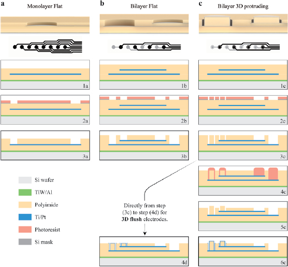
Figure 2. Fabrication process flow for monolayer flat (a), bilayer flat (b), and bilayer 3D electrodes. (c) Each column contains a schematic cross-section of the final electrodes (top), a top view of the used Pt design with the bottom layer marked in grey (second row), and the last main steps of the fabrication for the respective structures (following rows). (1(a)–(c)) Deposition of all PI and Pt layers and patterning of all the Pt layers; (2(a)–(c)) hard mask deposition, photolithography, and hard mask patterning; (3(a)–(c)) PI dry etching and mask removal; (4(c)): second photolithography; (5(c)): second PI dry etching; (6(c)) and (4(d)): pillars covering by Pt sputtering through a stencil.
Download figure:
Standard image High-resolution image2.2. Electrode characterization
The electrode arrays were imaged with light microscopy and scanning electrons microscopy (SEM). Image post-processing was performed using ImageJ.
Electrochemical impedance spectroscopy (IS) was performed with a potentiostat (Compact Stat, Ivium Technologies). The arrays were soaked in phosphate buffered saline (PBS, 1×) together with a Pt counter and an Ag/AgCl reference wires, the potential was set at 50 mV, and the impedance magnitude and phase were measured between 1 Hz and 1 MHz.
Cyclic voltammetry (CV) was performed with the same setup and three-electrodes configuration as for IS. The applied voltage was scanned between −0.6 and 0.8 V at a rate of 50 mV s−1 and the current was measured and averaged for each electrode (six cycles, the first cycle was discarded). The cathodic phase area (shaded area in figure 4(c)) was measured to determine the charges generated per cycle (area/scan rate) and the normalized cathodic charge storage capacity (CSC, charges/electrode surface area).
2.3. In vivo experiments
Animal experiments were performed according to the ethical authorization GE13416 approved by the Département de l'emploi, des affaires sociales et de la santé (DEAS), Direction générale de la santé of the Republique et Canton de Geneve, Switzerland. Two month old C57BL/6J mice (Charles River) were housed with a 12 h day/night cycle and with access to food and water was ad libitum. All the experiments were carried out during the day. Before the surgical procedure, mice were anesthetized with isoflurane inhalation (induction 0.8–1.5 l min−1, 4%–5%; maintenance 0.8–1.5 l min−1, 1%–2%). Analgesia was performed by subcutaneous injection of buprenorphine (Temgesic, 0.1 mg kg−1), and a local subcutaneous injection of lidocaine (6 mg kg−1) and bupivacaine (2.5 mg kg−1) with a 1:1 ratio. The depth of anaesthesia was assessed with the pedal reflex, the eyes were protected with artificial tears, and the temperature was maintained at 37 °C with a heating pad during both surgical and recording sessions.
Deeply anaesthetised mice were placed on a stereotaxic frame and the skin was opened. A squared craniotomy of approximately (4 × 4) mm was opened over the visual cortex (identified by stereotaxic coordinates) and the dura mater was removed. Bilayer multielectrode arrays were inserted in the visual cortex using a micromanipulator (SM-15R, Narishige), while a reference stainless-steel screw electrode was placed on the rostral side of the cranium, outside of the visual cortex. A needle placed subcutaneously in the dorsal area near the tail served as the ground (figure 5(a)). None of the implants was damaged by the insertion procedure and all the recorded data from all the electrodes were included in the statistical analysis. Ten light flashes (4 ms, 1–30 cd s m−2) were delivered with a Ganzfeld stimulator (BM6007B9.5, Biomedica Mangoni) positioned close to the contralateral eye and the corresponding visually evoked cortical potentials (VEPs) were amplified, filtered (0.1–300 Hz), and digitalized for 1000 ms (50 ms pre-stimulus and 950 ms post-stimulus) at 2 kHz (BM623, Biomedica Mangoni). The ipsilateral eye was not covered during stimulation. The signals were acquired simultaneously in four channels connected to four of the electrodes in the probe. VEPs signals were plotted in MATLAB R2015b (MathWorks) and peaks amplitudes, prominences, and latencies determined. For the evaluation of the signal-to-noise ratio (SNR), the standard deviation of the baseline was calculated within the first 50 ms of recordings prior to the flash stimulus (noise, N), while the full signal standard deviation was calculated for the entire 1000 ms of recordings (signal, S).
Animals were euthanized while still under anaesthesia by CO2 inhalation. In animals designated for brain imaging, the craniotomy was closed, and the animal was left implanted for one week before perfusion. Animals were then euthanized with an injection of pentobarbital (150 mg kg−1) under a chemical hood. The chest cavity was open to expose the beating heart and the descending aorta was clamped to deliver the fixative solution only to the brain. A needle was inserted in the left ventricle and the right atrium was cut to allow complete bleeding. The animal was immediately perfused with PBS followed by a fixative solution of 4% paraformaldehyde (PFA) in PBS. At the end of the procedure, the head of the animal was cut, and the brain removed and placed in 4% PFA for post-fixation.
2.4. Whole brain imaging
Brain clarification was performed according to a previously described procedure [26]. Briefly, after overnight post-fixation at 4 °C in PFA 4%, the brain was immersed in hydrogel solution (Acrylamide 40% + VA-044 initiator powder in PBS) at 4 °C for three days. The hydrogel polymerization was induced by keeping the sample at 37 °C for 3 h, then the brain was passively clarified in 4% sodium dodecyl sulfate clearing solution (pH 8.5) for four weeks under gentle agitation at 37 °C. The whole clarified brain was transferred to Histodenz solution at pH 7.5 (Sigma) and imaged with a light-sheet microscope.
To image the electrode array within the mouse brain, a custom-made light-sheet microscope optimized for labelled clarified tissue was used (Clarity Optimized Light-sheet Microscope, COLM, http://tomerlab.org/colm) [27]. The sample was illuminated (488 nm) by two digitally scanned light-sheets coming from opposite directions and the emitted fluorescence was collected by high numerical aperture objectives (Olympus XLPLN10XSVMP, N.A. 0.6) filtered (Brightline HC 525/50, Semrock) and imaged on a digital CMOS camera (Orca-Flash 4.0 LT, Hamamatsu) at a frequency ranging between 5 and 10 fps. A self-adaptive positioning of the light sheets across Z-stacks acquisition ensured an optimal image quality over up to 1 cm of tissue.
2.5. Statistical analysis
The computation of the mean, the standard deviation (s.d.) and the standard error of the mean (s.e.m.) of data distributions and the graphical representation of the results were performed with OriginPro 2017G (OriginLab). Statistical analysis was performed with a t-test or a non-parametric Mann–Whitney test depending on the results of the Shapiro–Wilk normality test. For each dataset, w is the number of the electrode, N is the number of animals, and n is the number of recordings (consecutive sweeps).
3. Results
The manufacturing method we have proposed to create multilayer 3D electrode arrays applies established wafer-scale processes in the field of microtechnology [6, 28, 29]. The multilayer 3D electrode arrays can be fabricated in two fashions: with flush or protruding electrodes. Compared to multilayer flat electrodes, the fabrication of 3D flush structures requires a single additional step of pillars covering (step (4d) in figure 2), as the photolithographic and etching steps only differentiate in the masking design. Three additional steps (4c, 5c, and 6c in figure 2) with respect to multilayer flat electrodes are required to fabricate the 3D protruding pillars of variable heights. The materials used to fabricate the arrays are PI as a substrate and Pt as a metallic conductor, two widely used materials in implantable medical devices. However, other polymers such as parylene C or PDMS could be used, as well as other conductive materials and coatings such as gold, iridium oxide, and Pt grey. Figure 1(d) shows a magnified cross-section view of a 3D protruding electrode. From this image, it is clear how the metallization of the pillar wall generates an electrical connection between the based electrode and the top surface of the pillar.
The differences in structure, electrode design, and fabrication process used to manufacture monolayer flat (a), bilayer flat (b), and bilayer 3D flush/protruding (c) electrode arrays are shown in figure 2. It is worth mentioning that bilayer arrays have the width (needed for interconnects) almost half the size of monolayer configurations. Consequently, for three layers, the difference would be of about 1/3. The 3D structures have been obtained by etching a ring in the encapsulation layer at the electrode location instead of etching the entire openings (figure 2 steps 2b and 2c), therefore creating a pillar on top of the base electrode. To make the pillar electrically conductive and connecting it with the base electrode, the pillar walls have been coated with Pt by sputtering (figure 2, steps 4d and 6c), which is known to deposit material in a relatively isotropic manner [30]. At this point, the electrode contact has been elevated to the pillar top surface and at the same level for all the layers. The difference in the fabrication between 3D flush and 3D protruding are two extra steps of photolithography (protecting the pillars, step 4c) and PI dry etching (lowering the overall encapsulation thickness, step 5c). Indeed, for protruding electrodes, one must deposit a thicker PI encapsulation layer corresponding to the desired pillar height and in prevision of the extra etching step.
A light microscopy image of the bilayer implants in figure 3(a) shows a fabricated eight-electrode array with an electrode diameter of 100 µm and a pitch size of 200 µm. Here, the Pt covering the pillars is perceivable, and the organization of the interconnects is visible through the PI, where they are appropriately aligned and therefore sparing a significant area of the implant. In the following part of the study, we focus only on 3D protruding electrodes. The choice is justified by the fact that their structure, although more complicated in terms of fabrication, may enable a better contact with the tissue [23, 24]. SEM pictures show a tilted view of three protruding electrodes together with a zoom into one of them (figures 3(b) and (c)). The electrode diameter is 100 µm with a pillar diameter of 76 µm, leading to a groove width of 8 µm. In this electrode array, the pillars have been fabricated with a protruding height of about 6.5 µm above the top PI surface (figure 3(d)). Note that, although the layers are placed at a different depth within the PI, the top contact sites for each electrode lay at the same height. In addition, the sputtered Pt covering the pillars (brightest material in figures 3(b) and (c)) surpasses the size of the opening and deposits on the encapsulation layer. This is because the hole design in the stencil had a diameter of 100 µm, matching the size of the contact at the pillars bottom. To obtain a more precise covering of the pillars, the sputtering through stencil could be replaced by lift-off or etching process. Figure 3(e) shows the roughness of the Pt-covered pillar surface after PI dry etching.
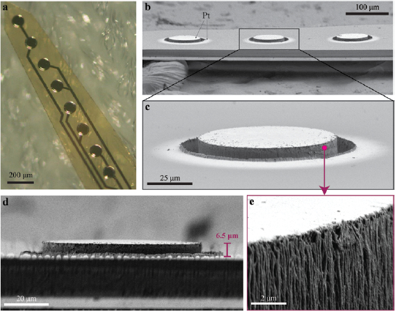
Figure 3. Micrographs of the fabricated bilayer probes. (a) Light microscopy image showing the 3D protruding electrodes and their Pt interconnects placed on two different layers and vertically aligned within PI. (b) SEM image of the 3D protruding electrodes (light coloured material: Pt. Tilting angle of 14° with respect to the side view). (c) Magnification over one 3D protruding electrode. (d) The same electrode looked by its side view, where the protruding height of 6.5 µm is visible. (e) Further zoom on the Pt-coated pillar revealing the side wall roughness.
Download figure:
Standard image High-resolution imageFigure 4 illustrates the electrochemical characterization of the fabricated electrode arrays, in a monolayer configuration, consisting of flat and 3D protruding electrodes. The purpose of these measurements is to validate 3D electrodes and establish possible differences with standard flat electrodes. IS (figures 4(a) and (b)) shows a typical electrode–electrolyte interface behaviour [5]. The most prominent difference is the decreased impedance magnitude over the tested range of frequencies for the 3D protruding electrodes (w = 19) with respect to the flat electrodes (w = 12). At 1 kHz, the impedance magnitude values (mean ± s.d.) are 194 ± 47 kOhm for 3D protruding electrodes and 427 ± 155 kOhm for flat electrodes (p < 0.0001, t-test), while the values for the phase are not significantly different at this frequency (−65.7 ± 4.0° for 3D protruding electrodes and −63.2 ± 7.7° for flat electrodes; p = 0.244, t-test). The lower impedance values can be justified by the difference in the electrode surface area: 0.0111 mm2 for 3D protruding and 0.0084 mm2 for flat electrodes. In addition, the 3D protruding electrodes show a more resistive behaviour at high frequencies (104–106 Hz). This may result from the lower spreading resistance of 3D electrodes, because of their higher surface area and protruding geometry. Electrochemical IS also showed no major differences between the bottom and top layers for 3D protruding electrodes in bilayer probes (p = 0.45, Mann–Whitney test).
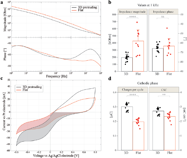
Figure 4. Electrochemical characterizations of 3D protruding and flat electrodes in PBS. (a) Bode plots of IS with the average magnitude (top) and average phase (bottom) for 3D protruding electrodes (w = 19) in black and flat electrodes (w = 12) in red. (b) Quantification (mean ± s.d.) of the impedance magnitude (t-test, p < 0.0001) and phase (t-test, p = 0.244) at 1 kHz. (c) Mean CV curves for 3D protruding electrodes (black, w = 18) and flat ones (red, w = 12), measured with a scan rate of 50 mV s−1. (d) Quantification (mean ± s.d.) of the charges per cycle (Mann–Whitney test, p < 0.0001) and CSC for the cathodic phase (Mann–Whitney test, p < 0.01) represented by the shaded area in (c).
Download figure:
Standard image High-resolution image
Figure 5. In vivo recordings with bilayer 3D protruding electrodes of VEPs. (a) Sketch of the experimental setting and probe implantation with the approximate depth into the visual cortex in µm. (b) Example of VEP recordings with a light intensity of 30 cd s m−2 (each trace is an average of n = 10 repetitions from N = 1 mouse). The vertical black line is the occurrence of the flash. (c) Expansion and superimposition of the traces of the first four electrodes of the graph in (b) (100–700 µm). Here, the arrows highlight the evolution of N1 and N2 peaks. (d) Absolute amplitude values of N1 and N2 peaks plotted versus the penetration depth (mean ± s.e.m., N = 3 mice; for each animal, n = 10 repetitions have been averaged).
Download figure:
Standard image High-resolution imageCV has been performed (figures 4(c) and (d)) within the Pt water window (−0.6 to 0.8 V) for 3D protruding electrodes (w = 18) with respect to flat electrodes (w = 12). It is visible in figure 4(c) that the measured currents extend to greater values for the 3D geometry. As for the impedance, this effect derives from an increased surface area, enabling a less impeded charge injection at the electrode–electrolyte interface [5]. Accordingly, the charges injected per cycle and their corresponding CSC are calculated for the cathodic phase from the area within the curves (figure 4(d)). The amount of charges generated for each cycle is higher for the 3D protruding electrodes (0.301 ± 0.024 µC for 3D and 0.197 ± 0.022 µC for flat; p < 0.0001, Mann–Whitney test). Interestingly, when normalized by the exposed surface area, the CSC of 3D electrodes remains slightly higher (2.71 ± 0.22 mC cm−2 for 3D and 2.34 ± 0.26 mC cm−2 for flat; p < 0.01, Mann–Whitney test), even though it should not differ, as it is made of the same material. This difference could be due to the roughness of the pillar walls appearing after PI dry etching, which further augments the surface area of 3D electrodes. Figure 3(e) provides an SEM picture of the Pt-coated roughness on a pillar wall. Table 1 shows the values mentioned above of surface areas, cathodic charges (from CV), and cathodic CSC for both 3D protruding and flat electrodes. Moreover, it shows the absolute and the percentage differences of the measurements together with the percentage quantity that is not due to the geometrical surface area of the electrodes (32%), but it likely represents the roughness contribution. As the calculated increase from the charges (21%) slightly differs from the amount obtained directly from the cathodic CSC difference (16%), we inserted in the table the average value between these two, which represents a probable increase in active surface area due to roughness (18.5%). Accounting this, the more realistic increment in the active surface area from flat to 3D electrodes is about 50%, which further augments the electrode–electrolyte contact area and leads to a higher charge storage capacity and to a lower impedance.
Table 1. Values for surface area, charges generated during the cathodic phase of CV, and cathodic CSC for the 3D protruding and flat electrodes. The absolute and percentage differences between the two types of electrodes are also shown. The last column shows the percentage difference that cannot be attributed to the 3D geometry, therefore likely due to roughness.
| 3D | Flat | Difference | Difference (%) | Roughness contribution (%) | |
|---|---|---|---|---|---|
| Surface area (mm2) | 0.0111 | 0.0084 | 0.0027 | 32 | |
| Charges (µC) | 0.301 | 0.197 | 0.104 | ~53 | 53–32 = 21 |
| CSC(mC cm−2) | 2.710 | 2.337 | 0.373 | ~16 | 16 |
| Average (%) | 18.5 |
Bilayer 3D protruding arrays have been used to record VEPs in mice upon ganzfeld flash stimulation. Figure 5(a) shows a sketch of the experiment with the implant location and approximate depth into the visual cortex of the eight-electrode array. The insertion of the probe was stopped once the last electrode disappeared into the brain surface, therefore—assuming that the implant did not bend inside the brain—we can approximate the location of each electrode using the array pitch size of 200 µm. Hence, the different recording depths were at about 100, 300, 500, 700, 900, 1100, 1300, and 1500 µm below the cortical surface. The mouse visual cortex is about 1.2–1.3 mm thick [31, 32], meaning that the two terminal electrodes (at 1300 µm and 1500 µm) could presumably lay in the white matter or the transition region. Nevertheless, considering that a perfectly vertical and straight insertion of a flexible implant hardly represents the real scenario, most likely at least one of these electrodes is still found in the deep layers of the visual cortex. Figure 5(b) shows an example of VEP recordings of all the eight electrodes upon a flash illumination of 30 cd s m−2. Each trace represents the average of n = 10 consecutive recordings (1 Hz repetition rate) from N = 1 mouse. Peaks characteristic of the VEPs (N1, N2, and N3 respectively) are visible at 50–90 ms, as well as 100 ms, and 110–150 ms post-stimulus [33]. Peak amplitude and latency shift as the recordings were taken more profound in the cortex. The amplitude (in case of N1, N3) and polarity (in case of N2) of the electrode at 1500 µm are very dissimilar from the others, probably because it is located below the cortical layers. For better visualization and comparison of depth effects, the traces of the first four electrodes (100–700 µm) are enlarged and superimposed in figure 5(c). Negative (N1, N2, N3) and positive peaks (P1, P2) are identified. As the depth into the cortex increases (black arrows): N1 decreases its amplitude, while N2 increases it. In panel (d), the mean (±s.e.m., N = 3 mice) amplitude values of N1 and N2 are plotted versus the penetration depth.
VEP traces (average of n = 10 repetitions from N = 1 mouse) of the eight electrodes recorded at light intensities of 1, 5, 10, and 30 cd s m−2 are presented in figures 6(a)–(d), and N1 and N2 latencies and prominences have been identified and plotted versus the light intensity (N = 3 mice) in figures 6(e)–(h). The characteristic evolution of the VEP peaks can be observed. The increase of N1 amplitude and the decrease of latency with light intensity, as well as the opposite behaviour of N1 and N2 amplitudes with recording depth are known phenomena of local field potentials recorded in the visual cortex [33–35]. Upper and lower regions of the cortex approximately follow the same trend, apart from N1 prominences (figure 6(g)), where the upper region (100–700 µm) responses continuously augment with light intensity, which is a contrasting behaviour with respect to the other prominence trends.

Figure 6. Evolution of field potential peaks while varying the light intensity. (a)–(d) Examples of VEPs recorded at the eight depths for different light intensities of 1, 5, 10, and 30 cd s m−2, respectively (each trace is an average of n = 10 repetitions from N = 1 mouse). The vertical black lines are the occurrence of the flash. Mean (±s.e.m.) of latencies (e) and (f) and prominences (g) and (h) of N1 and N2 peaks depending on flash intensity and cortical depth (N = 3 mice; for each animal, n = 10 repetitions have been averaged).
Download figure:
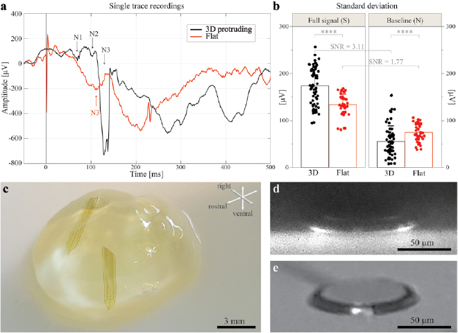
Standard image High-resolution imageAfter analysis of the single sweep recordings (n = 1), it is possible to observe more defined peaks with bilayer 3D structures with respect to the monolayer flat electrodes, where the peaks are less evident and not unequivocally identifiable (figure 7(a)). To further characterize the SNR of the 3D electrodes compared to the flat ones, the s.d. of the single recording traces of each type of electrodes have been calculated for the full signal (S) and the pre-stimulus baseline (N). For bilayer 3D electrodes, n = 72 recordings obtained from w = 8 electrodes and N = 1 mouse have been considered. For monolayer flat electrodes, n = 40 recordings obtained from w = 4 electrodes and N = 1 mouse have been considered.
Figure 7. Signal quality and in-brain visualization of the bilayer 3D protruding electrodes. (a) Example of single trace recordings with a light intensity of 30 cd s m−2 of bilayer 3D protruding (black) and monolayer flat (red) electrodes. The vertical black line is the occurrence of the flash. The large and fast peak visible in the red trace is a stimulation artefact. (b) Signal quality evaluation by means of s.d. (mean ± s.d.) of the traces for the full signal (S) (Mann–Whitney test, p < 0.0001) and for the baseline (N) (Mann–Whitney test, p < 0.0001) of bilayer 3D protruding electrodes (n = 72 recordings obtained from w = 8 electrodes and N = 1 mouse) and monolayer flat electrodes (n = 40 recordings obtained from w = 4 electrodes and N = 1 mouse). All the recordings were taken with a light intensity of 30 cd s m−2. (c) Photograph of a clarified mouse brain with two monolayer 3D protruding probes implanted. (d) Light sheet micrograph of a 3D protruding electrode within the clarified mouse brain. (e) Micrograph of a 3D protruding electrode prior to implantation.
Download figure:
Standard image High-resolution image
The signal after the light stimulus has larger peaks for 3D protruding electrodes with respect to flat (174 ± 39.7 µV for 3D protruding electrodes and 133 ± 23.7 µV for flat electrodes; p < 0.0001, Mann–Whitney test), while the baseline has a lower s.d. indicating a lower noise level (56 ± 32.9 µV for 3D protruding electrodes and 75 ± 19.3 µV for flat electrodes; p < 0.0001, Mann–Whitney test). The s.d. of the full signals divided by the one of baselines (SNR) gives 3.11 for the 3D protruding electrodes and 1.77 for the flat electrodes (figure 7(b)).
During surgical implantation, the 3D protruding electrodes may be damaged by frictions between the protruding pillar and the brain parenchyma. To further verify the integrity of the 3D protruding electrodes within the tissue, the arrays have been imaged inside a clarified mouse brain using a light-sheet microscope. Figure 7(c) contains a photograph of the transparent brain with two implanted monolayer 3D electrode arrays used to image the structures as shown in figure 7(d). In this micrograph, the 3D protruding electrode is recognizable intact, within the brain tissue (black in the image). For comparison, figure 7(e) illustrates a similar electrode imaged with a light microscope before implantation.
4. Discussion
In this article, we have proposed an electrode array design that can be used to optimize neural implant with high electrode density, reduced probe size, and small electrode-tissue distance. Multilayer 3D electrode arrays do not require a further significant amount of resources and fabrication steps with respect to flat electrodes; however, their contribution to recording and stimulation capabilities could be significant. The 3D protruding pillars could better reach target neurons separated from the stimulating or recording sites by the fibrotic tissue surrounding the implant [24, 36]. An additional advantageous feature of these 3D electrodes (both flush and protruding) is that all sites have the same elevation concerning the global thickness of the implant, independently of the different planes at which they were placed originally with their respecting traces. Moreover, there is no need for electroplated electrodes that are difficult to control, demand considerable material deposition, and rigidify the implant [37].
The proposed fabrication method allows for the production of pillars with a protrusion height between 0 (flush) and 30 µm for up to four electrode layers. Two major aspects must be considered when fabricating geometries with high aspect ratios, as in the case of pillar height to groove width ratios above 3. First, it could be difficult to etch away the polyimide at the bottom of the groove even with high over-etching times. Second, the covering of the metal by sputtering could not be as homogeneous as for geometries with lower aspect ratio, and this could lead to poor electrical contact between the bottom and the top of the pillars. Another factor limiting the number of layers is that the polyimide etching to create the grooves is concluded before for the first level and then for the underlying layers. This means that the Pt, acting as an etch stop layer, must withstand the plasma treatment until the bottom level is entirely etched. Although Pt is a suitable etch stop material for oxygen plasma [38], the directional ion bombardment could damage or thin the Pt after prolonged exposure. Possible ways to circumvent this problem are either to augment the thickness of Pt depositions to compensate the loss during etching or to deposit another etch stop layer after Pt (such as Si or SiO2) and remove it before the covering of the pillars.
Here, PI and Pt have been used as insulating and conducting material respectively, but other insulators and conductors can be also used to fabricate these electrode arrays.
In general, low impedance electrodes are preferred for recording neural activity, while electrodes with high charge storage/injection capacity are advantageous for stimulation [5]. As they both are influenced by the electrode–electrolyte interface, augmenting the surface area (i.e. porosity, roughness, geometry) improves both characteristics. As visible from electrochemical measures, the 3D electrodes provide a better option compared to the flat ones for both recording and stimulation.
In vivo recordings of VEPs with 3D protruding electrodes have shown a better SNR with respect to flat electrodes, thus allowing a detailed characterization of all the VEP peaks depending on the electrode depth in the brain and the light intensities.
High-resolution imaging of multielectrode arrays within the brain showed that the 3D protruding electrodes are intact after one week of implantation.
In conclusion, the 3D electrode arrays allow a multilayer placement of their interconnects within a flexible substrate, thus reducing the size of the probe per the same number of electrodes. In addition, all the electrode sites are maintained at the same level and nearer to the tissue. The surface area of the electrodes is increased by about 50% compared to flat electrodes, which leads to a lower electrochemical impedance and a higher charge storage capacity.
To further characterise these multilayer 3D electrode array, the next step will include in vivo chronic recordings and post mortem histological investigations. VEP recordings at different time points will be necessary to evaluate the long-term stability of the 3D pillars. Immunofluorescence assays will be instrumental to assess the extension of the glial scar and the incorporation of the protruding 3D electrodes within the brain tissue. Additional optimization steps could involve the fabrication of taller protruding electrodes with highly porous coatings (e.g. conductive polymers or conductive hydrogels [39]) to further reduce the electrochemical impedance and to better interface the stiff array with the soft biological tissue.
Acknowledgments
This work has been supported by École Polytechnique Fédérale de Lausanne and Medtronic. The authors would like to thank the staff of the EPFL Center of Micronanotechnology (CMi) and Bastien Duckert for their support related to microfabrication processes. We would like to thank also the Imaging and Light Microscopy Facility of the Wyss Center for Bio- and Neuroengineering and Elodie Geneviève Meyer for their help with the light-sheet microscopy.
Authors contribution
MJIAL designed the fabrication strategy, fabricated the samples, performed the characterizations, and analysed the data. PV performed the in vivo validation and the whole-brain imaging. DG supervised the study. MJIAL wrote the manuscript. PV and DG edited the manuscript.