

Abstract
We present a method to determine the internal quantum deficiency (IQD) of a predictable quantum efficient detector (PQED) based on measured photocurrent dependence on bias voltage and a 3D simulation model of charge carrier recombination losses. The simulation model of silicon photodiodes includes wafer doping concentration, fixed charge of SiO2 layer, bulk lifetime of charge carriers and surface recombination velocity as the fitted parameters. With only one set of physical photodiode defining parameters, the simulation shows excellent agreement with experimental data at power levels from 100 μW to 1000 μW with variation in illumination beam size. We could also predict the dependence of IQD on bias voltage at the wavelength of 476 nm using photodiode parameters determined independently at 647 nm wavelength. The fitted values of doping concentration and fixed charge extracted from the simulation model are in close agreement with the expected parameter values determined earlier. At bias voltages larger than 5 V at the wavelength of 476 nm, the internal quantum efficiency of one of the tested PQEDs is measured to be 0.999 970 ± 0.000 027, where the relative expanded uncertainty of 0.000 027 is one of the lowest values ever achieved in spectral responsivity measurement of optical detectors.
Export citation and abstract BibTeX RIS

Original content from this work may be used under the terms of the Creative Commons Attribution 4.0 licence. Any further distribution of this work must maintain attribution to the author(s) and the title of the work, journal citation and DOI.
1. Introduction
Predictable quantum efficient detectors (PQEDs) are silicon trap detectors based on self-induced photodiodes in a wedge trap structure [1–3] which reduces the reflection losses to typically lower than 50 parts per million (ppm) over the spectral range from 400 nm to 900 nm for p-polarised light. The special design of the photodiodes with a thin self-induced doping free inversion layer, generated by the fixed charges in the SiO2 passivation layer, produces a shallow depletion region in p-type silicon [1]. Inverted design with Al2O3 passivation layer on n-type silicon has also been realised [4]. With this simple structure [5], very low internal charge-carrier losses of the photodiodes—less than 100 ppm can be achieved [2, 6, 7]. The PQED is therefore an excellent approximation of an ideal quantum detector where each incident photon generates an electron hole pair to be measured in the external circuit at a sufficiently high bias. Its responsivity is given as

where e is the elementary charge, h is Planck constant, c is the speed of light in vacuum, ρ(λ) is the spectrally dependent reflection loss and δ(λ) is the spectrally dependent internal quantum deficiency (IQD) corresponding to the charge-carrier losses. As seen from equation (1), if the reflection and internal losses approach zero, the spectral responsivity of the PQED is given by the values of fundamental constants and vacuum wavelength λ. This makes the PQED a very attractive radiant power measurement standard as a simple current measurement at a known wavelength gives the radiant power constantly from the fundamental constant ratio. The PQED has therefore been included in the mise-en-pratique for the definition of the candela [8] as one possible primary standard based on a different technology than the most commonly used cryogenically cooled electrical substitution radiometer [9].
The responsivity of PQED has shown to be extremely stable with an undetectable drift over ten years [10] in the comparison to high accuracy cryogenic radiometers. At the lowest uncertainty levels, below 100 ppm, potential drift in the photodiodes responsivity due to the change in the IQD is hard to measure. Specular reflectance losses, on the other hand, can be determined with relative measurements within a ppm [1] and non-existence of diffuse reflectance losses caused by dust particles can be confirmed from a uniformity scan with a small laser beam [3]. This leaves quantification of the IQD by stand-alone independent measurement techniques as the main challenge of the PQED responsivity determination. Earlier approaches to IQD determination include the water-drop method in the original self-calibration procedure [11], purely relative measurements between photodiodes and spectrally invariant detectors [12], simulations with 1D charge-carrier transport software [7], and 3D simulations at narrow wavelength and radiant power range [4]. The two latter methods are predecessors of the present work, but they suffer from high uncertainty in the method and validation of the results.
We present here a method exploiting the simple structure of the PQED photodiodes and three-dimensional computer simulation models to independently extract the photodiode IQD from a set of relative photocurrent measurements over a wide range of bias voltages, radiant power levels and wavelengths. We test the validity of the results on IQD by applying the obtained photodiode parameters to other measurement conditions, such as different beam size and wavelength, and achieve excellent agreement between experimental data and simulations in the new conditions.
2. Photodiodes and measurements
The design, manufacturing and characterization of PQED photodiodes used in this paper are presented in [1]. The photodiode is fabricated from a 525 μm p-doped silicon wafer with 2 × 1012 cm−3 doping concentration. The photodiode has an active area of 11 mm × 22 mm. A SiO2 layer is deposited on top of the silicon substrate to create a surface area with trapped charges. Both cathode and anode contacts are placed on the front side of the photodiode. Manufacturer characterizations in 2010 show that the photodiodes have surface charge density of 6.2 × 10¹¹ e cm−2. In order to obtain low specular reflectance losses, PQED is constructed from two photodiodes in a light trap configuration as shown in figure 1. The incoming light beam hits the first photodiode with an angle of 45°. The angle of 15° between the two photodiodes helps to confine the light beam inside the PQED with seven reflections before the beam leaves the PQED along the same path as the incoming beam.
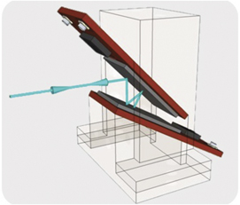
Figure 1. PQED with two photodiodes in light trap configuration. Reproduced from [1]. © 2013 BIPM & IOP Publishing Ltd. All rights reserved.
Download figure:
Standard image High-resolution imageThe PQED's IQD is measured by using a setup as illustrated in figure 2. An ultra-stable (20 ppm h−1) quasi-Gaussian low scatter laser beam impinges the PQED under test. The bias voltage applied to the PQED is generated by a voltage calibrator (voltage accuracy better than 20 μV). The photocurrents from both photodiodes are coupled in parallel and converted to voltage by a calibrated transimpedance amplifier (TIA) of which output voltage is measured by an 81/2 digits voltmeter. The linearity of the TIA current-voltage conversion over the ranges utilized during the measurement has been evaluated to be better than 0.01%. The beam profile is acquired via a charge-coupled device (CCD)-camera-based laser beam profiler placed on a motorized linear stage.
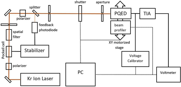
Figure 2. Automated facility schema for the measurement of the PQED's IQD.
Download figure:
Standard image High-resolution imageThe PQED is placed on a four degrees of freedom precise adjustable stage. Its orientation relative to the beam is adjusted using the back reflected light leaving the wedge structure of two PQED photodiodes (figure 1). The PQED's horizontal and vertical center positions relative to the beam are extracted from the calculation of the center of mass of the photocurrent signals recorded while moving the detector ±6 mm horizontally and vertically from the visually determined central position such that the laser beam overlaps the 10 mm-diameter optical input aperture of the PQED. The measurement of the PQED photocurrent at one bias voltage value includes the integration of recorded signal up to 4 s both when the laser impinges the detector and when the shutter is closed. The latter dark signal is then subtracted from the light signal to take into account the bias voltage dependent dark current contribution of the PQED. A delay of 2 s is used after the shutter is actuated to let the photocurrent signal stabilize. The bias voltage range spans from 0 V to 20 V with a 50 mV step from 0 V to 1 V, 100 mV from 1 V to 6 V and 500 mV from 6 V to 20 V. The Gaussian collimated laser beam diameter is adjusted to a standard deviation value (σ) of about 0.6 mm where 2σ is the radius at which the light intensity falls down to 1/e2 of the beam axial value. As mentioned above, the actual spatial structure of the laser beam is measured using the beam profiler. The laser beam power level is adjusted manually to perform the measurement at 100 μW, 200 μW, 350 μW, 600 μW and up to 1000 μW. Two adjustable apertures are placed in front of the detector to minimize residual stray light surrounding the laser beam. A fully automated measurement procedure changes the bias voltage, measures the photocurrent signal and closes/opens the shutter.
3. Simulation model
3.1. Simulation model
Charge carrier transport in 3D model is simulated by using Cogenda Genius Device Simulator [13]. Figure 3 shows an illustration of the simulation structure with the intention of replicating the actual photodiode structure. Only 1/8 of the real device is used in the simulation model due to limited computational resources. Based on the actual size of photodiode, the simulation structure has the size of 5500 μm × 5500 μm. The structure includes a p-doped silicon substrate, p-doped and n-doped 100 μm wide contacts for electrical connection separated 300 μm apart. A SiO2 layer is placed on top of the silicon substrate to create trapped surface charge area. The rear side of the silicon substrate is heavily p-doped. Detailed information about the photodiode structure can be found in [1]. The whole structure is illuminated at the corner with 1/4 of the radiant power, which represents an illumination at the center of the photodiode. A flat top uniform illumination area is calculated from the measured Gaussian-like light beam used in the experiments with an incident angle of 45 degrees generating an elliptical spot on the photodiode.
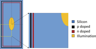
Figure 3. Illustration of simulation structure.
Download figure:
Standard image High-resolution imageThe IQD caused by charge carrier recombination is calculated by:

where Rsurf is the total surface recombination rate, Rbulk is the bulk recombination rate of electron–hole pairs and Gopt is the total rate of optical generation of charge carriers. The charge carriers are generated within the photodiode volume according to the illumination area and spectral attenuation of the light beam in silicon [14]. Even though measured at a 45 degrees angle of incidence, the beam direction will deviate only about 10 degrees from the surface normal inside the photodiode due to silicon's high refractive index. This corresponds to a penetration difference to normal incidence of less than 1.6% and is not corrected for in the generation distribution.
3.2. Cylindrical beam approximation to a Gaussian beam
The simulation software is not capable of implementing a Gaussian illumination beam profile, so uniform illumination beam conversion is necessary to generate an approximation to a Gaussian beam. A Gaussian beam may be defined in various ways. We define throughout the manuscript 2σ as the beam radius at which the light intensity falls down to 1/e2 of the beam axial value. A 2D Gaussian cross-section of the intensity profile of a light beam with intensity amplitude Io and standard deviation σ as shown in figure 4 is described as

where r is the radial distance from the center of the beam. The volume of a 3D Gaussian beam represents the total number of photons in the beam


In a flat top cylindrical beam approximation, we want the cylindrical beam amplitude to match the Gaussian beam amplitude and calculate the radius such that it has the same volume as the Gaussian beam. The volume of a cylinder with radius R with the same amplitude Io as the Gaussian light beam intensity profile is

This means that the volume of a cylinder, representing the approximation of the profile of a Gaussian beam with the same amplitude, has a beam radius R relative to the Gaussian beam width σ as

With this approximation, we have a conversion of a flat top simulation beam to a measured Gaussian beam with any σ value. For elliptical Gaussian beams, we use the standard deviations σx and σy along the principal axes.

Figure 4. Cross-section of a 3D Gaussian laser beam intensity profile, approximated by a cylinder of radius R =  . Also full width at half maximum and standard deviation σ of the Gaussian are displayed.
Download figure:
Standard image High-resolution image3.3. Calculation of optical absorption on the first photodiode of PQED
In a seven reflections PQED trap detector, the first photodiode has an oxide thickness of about 301.6 nm and the second photodiode has an oxide layer of about 220.6 nm [1, 15]. The first photodiode absorbs 85.7% and 85.9% of the total radiant power at 476 nm and 647 nm, respectively. This means that the first photodiode absorbs about six times the power of the second photodiode, as also confirmed by the photocurrent ratio measurements between the two photodiodes [3]. Thus, when measuring the photocurrent as a function of bias voltage, the I–V curve is defined by the response of the first photodiode as for instance in a 700 μW laser power measurement 600 μW is absorbed by the first photodiode and 100 μW is absorbed by the second photodiode. Unless operated close to the bias voltage where saturation in the response occurs, the IQD of the first photodiode is orders of magnitude higher than that of the second photodiode. This means that it is the first photodiode that defines the structure and shape of the response in a relative I–V measurement. In our simulations, we have used the approximation that about 86% of the applied laser power is absorbed by the first photodiode and this represents the I–V measurement at each power level for the PQED.
4. Results and discussion
4.1. Estimation of internal quantum deficiency
The aim of the work is to fit a 3D simulation model to experimental data to extract the value of IQD. An illustration of a photocurrent measurement with increasing reverse bias voltage is given in figure 5. In order to perform a fit of an IQD model to experimental data, the experimental data has to be converted to an IQD value according to [16]

where I(V, λ) is the measured photocurrent of a photodiode at bias voltage V and Iideal is the photocurrent from an ideal photodiode with vanishing IQD at a given absorbed radiant power Φ. Iideal can be related to other parameters as

The expected measured current from a photodiode with an unknown internal loss δ(V, λ) is given by

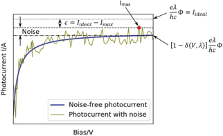
Figure 5. Photocurrent as a function of reverse bias voltage.
Download figure:
Standard image High-resolution imageIn the experiment, the ideal photocurrent Iideal is unknown and a correct representation of δ(V, λ) of equation (8) is possible only after Iideal is determined. However, it is known that the expected IQD at high bias voltages is small. We use the maximum measured photocurrent Imax to facilitate the fitting process and a parameter describing the small difference between Iideal and Imax is introduced by  = Iideal − Imax as shown in figure 5. Equation (8) then becomes

By defining offset parameter ξ(λ) as ξ(λ) = /Imax, equation (11) can be rearranged as


Since ξ(λ) ≪ 1, the term δ(V, λ)ξ(λ) can be neglected relative to δ(V, λ). Equation (13) becomes

Equations (2) and (14) form a consistent set of simulation values and experimental data to be used in presenting the figures of the next sections. The offset has a significant effect only at high bias voltages where the IQD is low. The offset parameter ξ(λ) = /Imax can be positive or negative depending on noise level in the measurement and IQD of the PQED.
4.2. Fitting simulated IQD to experimental data
Measured photocurrents I(V, λ) at different power levels from 100 μW to 1000 μW as a function of bias voltage V are used for determining IQD from the experimental data. The wide dynamic range is used because the fitting parameters have various sensitivities at different power levels. The I(V, λ) curves of two different PQEDs are measured by two different laboratories at wavelengths of 647 nm and 488 nm. PQED 1 is characterized at 647 nm. The experimental Gaussian beam profile is circular with a 1/e2 diameter of 2680 μm (σ = 670 μm), while PQED 2 is characterized at 488 nm with beam profile that is slightly elliptical with σ values of 267 μm (σx ) and 242 μm (σy ) in two principal axes. The equivalent flat top beam sizes used in the simulation are calculated from the experimental beam sizes by equation (7) as explained in section 3.2.
Figures 6(a) and (b) show experimental data and fitting results of PQED 1 and PQED 2, respectively. All simulations use materials data values for 300 K. The simulation result is fitted to experimental data by rewriting equation (14) as

The left-hand side of equation (15) is determined by the simulation results using fitted parameters. The right-hand side of the equation is calculated from experimental data. The fitting is a manual trial and error process based on the known sensitivity of the IQD prediction to the fitting parameters. Typically, the simulation is started by adjusting the values of fixed charge density Qf and surface recombination velocity (SRV) to match the corner points of the highest power curves as indicated with dashed circles in figure 6. Change of the fixed charge Qf shifts the corner points horizontally, whereas SRV shifts the corner points vertically. Then the remaining parameters defining the simulated IQD, i.e., bulk lifetime τbulk and substrate doping concentration p, are adjusted to all experimental curves to form a consistent set between simulation and experimental data, as different parameters dominate in different parts of the curves.

Figure 6. Fitted simulated IQD, δ (solid lines on primary axis) with experimental data, 1 − I/Imax + ξ (secondary axis) of PQED 1 at 647 nm (a) and of PQED 2 at 488 nm (b) with fitting parameters listed in table 1. The dashed circles indicate the corner point positions where recombination losses contribution from the back side of the photodiode ceases to influence. The corner points are used to determine initial values of Qf and SRV.
Download figure:
Standard image High-resolution imageThe offset ξ(λ) is determined by matching the saturated IQD at high bias voltages between simulation and experimental data of the right-hand side of equation (15). Noise may affect the offset via = Iideal − Imax (see figure 5). However, the results of the fitting process are insensitive to the exact value of Imax. If the data point corresponding to Imax is removed and the fitting process is carried out using the second largest experimental current value, the values of ξ(λ) and change in such a way that the left and right side of equation (15) agree. The saturation level IQD as well as values of the fitted parameters fixed charge Qf, SRV, bulk lifetime and doping concentration remain unchanged.
Taking into account the rough beam shape approximations we needed to do, remarkably good agreement between experiment and simulation is obtained in figure 6 for both PQEDs, with radiant power varying by one order of magnitude and δ(V, λ) varying by more than four orders of magnitude. The effect of approximating the Gaussian laser beam profile with the flat top profile is considered in more detail in appendix
Table 1. Experimental and fitted parameters of PQED 1 and PQED 2.
| Parameters | PQED 1 | PQED 2 |
|---|---|---|
| Wavelength λ—measured | 647 nm | 488 nm |
| Substrate doping p—fitted | 1.60 × 1012 cm−3 | 1.95 × 1012 cm−3 |
| Fixed charge density Qf—fitted | 4.5 × 10¹¹ e cm−2 | 3.0 × 10¹¹ e cm−2 |
| Bulk lifetime τbulk—fitted | 2.5 ms | 2.5 ms |
| SRV S0—fitted | 5000 cm s−1 | 3000 cm s−1 |
| Offset ξ(λ)—fitted | −15 ppm | 0 ppm |
4.3. Effect of beam size on IQD
In order to investigate the influence of beam size on PQED responsivity, a test on PQED 2 with a larger beam size than beam 1 used for the measurement result of figure 6(b) is performed. The new illumination beam 2 has σ values of 490 μm in both principal axes. This means that the diameter of beam 2 is approximately twice that of beam 1. Other parameters of beam 2 are close to those of beam 1 as described in table 2.
Table 2. Illumination beam parameters of PQED 2 in measurements with two beam sizes.
| Parameters | Beam 1 | Beam 2 |
|---|---|---|
| Wavelength | 488 nm | 476 nm |
| Radiant power | 560 μW | 510 μW |
| σx | 267 μm | 490 μm |
| σy | 242 μm | 490 μm |
Effect of the beam size on the IQD is shown in figure 7. By using the same fitted parameters to the experiment as with beam 1 on PQED 2, the simulation model well predicts measurement result at 510 μW radiant power with beam 2 parameters. This supports the conclusion that our beam approximation method is valid as the simulation results are in good agreement despite a significant change in the photocurrent response with bias voltage in the two experiments of figure 7. A large beam size offers lower IQD at the same bias voltage and the IQD reaches the saturation level at lower bias voltages as compared to a small beam size. However, the illumination beam size does not affect the saturation IQD level at high bias voltages. As described in appendix

Figure 7. Effect of the illumination beam size on the IQD of PQED 2 with parameters listed in tables 1 and 2. The data with beam 1 is reproduced from figure 6(b).
Download figure:
Standard image High-resolution image4.4. Effect of wavelength on IQD
To validate the simulation model, simulation with change in illumination wavelength is also examined. Measurements of PQED 1 are carried out at an additional wavelength of 476 nm at different radiant power levels from 100 μW to 843 μW in a similar way as the measurements at 647 nm in figure 6(a). The experimental beam has σ values of 630 μm in one principal axis and of 610 μm in the other principal axis. The beam sizes used for the measurement at 476 nm and at 647 nm (σ = 670 μm) are therefore quite close to each other. Hence, comparison of the experimental IQD in figures 6(a) and 8 reveals mainly the effect of wavelength variation. The fitted parameters of PQED 1 at 647 nm in table 1 are used for the simulation at 476 nm without any additional adjustment except for the change of offset ξ(λ) from −15 ppm at 647 nm to 0 ppm at 476 nm.

Figure 8. Simulated IQD, δ (solid lines on primary axis) of PQED 1 at 476 nm with fitting parameters from table 1 except ξ (476 nm) = 0 ppm compared to experimental data, 1 − I/Imax + ξ of PQED 1 (secondary axis) at 476 nm.
Download figure:
Standard image High-resolution imageThe simulation well predicts the experimental data at 476 nm in figure 8 using the detector parameters extracted from the fit at 647 nm. Although the simulation of 843 μW radiant power shows a small deviation with experimental data, the results support the conclusion that the extracted parameters are defining the response of the detector. The slight deviation may be due to uncontrolled differences in beam shape and beam size between the two wavelengths. The used flat top approximation of a Gaussian beam profile reduces simulation accuracy at both wavelengths.
4.5. IQD sensitivity to fitted parameters
The IQD sensitivity to simulation parameters and simulation uncertainty of PQED 1 are shown in figure 9. In the sensitivity and uncertainty analysis, wavelength 476 nm is used as the predicted response is compared to measured data. The simulation is performed at 201 μW (solid lines) and 601 μW (dashed lines) of radiant power. The fitted parameters of table 1 are varied so that the experimental data  of equation (15) lie between the lower and upper envelope curves provided by the left-hand side of equation (15) in the bias voltage range where curves are influenced by the fitted parameters. In general, the IQD is more sensitive to the change of parameters at high radiant power levels and each parameter affects the IQD curve differently. In the case of figure 9, the nominal offset ξ(λ) is zero and the left-hand side of equation (15) is equal to the IQD.

Figure 9. Change in δ(V, λ) − ξ(λ) (equation (15)) for PQED 1 at 476 nm with SRV S0 (a), with fixed charge Qf (b), with bulk lifetime τbulk (c), with doping concentration p (d), and with offset ξ(λ) (e) at radiant power levels of 201 μW (solid lines) and 601 μW (dashed lines). Quadratically combined envelope curves of (a) to (e) are shown in (f).
Download figure:
Standard image High-resolution imageAs shown in figure 9(a), the SRV changes the IQD at bias voltages above the corner point where the back surface recombination ceases to influence (highlighted by dashed circles in figure 6). The change in IQD with SRV at bias voltages just above this point is most sensitive at high radiant power. By changing SRV, the corner point is shifted vertically. SRV also influences the saturation level of IQD at higher bias voltages in the tens of ppm range. The value of Qf affects the whole IQD curve. In contrast to SRV, Qf shifts the corner point horizontally. Therefore, the corner point at high radiant power is used to determine the initial fit values of Qf and SRV as mentioned in section 4.2. Bulk lifetime variation changes the IQD curve mostly at low bias voltages well below saturation of IQD and is more dominant at low power levels compared to SRV. Doping concentration shifts the whole IQD curve, similar to Qf, except that just before saturation of IQD the relative sensitivity is much higher than that of Qf and that at high bias voltages the saturation IQD stays unchanged. The change of the offset only influences the saturation level of the curves as shown in figure 9(e). The offset values are chosen so that the change in saturation levels caused by offset matches the change in saturation levels caused by SRV in figure 9(a).
As compared to the best fit S0 value of 5000 cm s−1 shown in table 1 for PQED 1, the value of S0 ranges between 2000 cm s−1 and 8000 cm s−1 for the lower and upper envelope curves of figure 9(a). For the envelope curves, the Qf varies between 3.5 × 10¹¹ e cm−2 and 5.0 × 10¹¹ e cm−2 while bulk lifetime τbulk takes values between 1.5 ms and 3.0 ms. The corresponding nominal values from table 1 are 4.5 × 10¹¹ e cm−2 and 2.5 ms, respectively. The substrate doping varies between 1.45 × 1012 cm−3 and 1.65 × 1012 cm−3 in figure 9(d), while the nominal value from table 1 is 1.60 × 1012 cm−3. Offset ξ(λ) varies between −20 ppm and +20 ppm in figure 9(e).
Combining the lower and upper uncertainty estimates of separate individual simulation parameters of figures 9(a)–(e) generates expanded uncertainty bands for the predicted IQD that are shown in figure 9(f). The expanded IQD uncertainty contributions at 476 nm from each of the simulation parameters as half of the difference between the upper and lower envelope curves in figure 9 at 6 V reverse bias are listed in table 3. Possible errors due to the TIA described in section 2 have only a minor contribution, because the effect of nonlinearities is largely cancelled in the ratio I(V, λ)/Imax in equation (15). From the simulation point of view, the position of the beam on the photodiode is not critical unless the beam approaches the active area boundaries of the photodiode. When the bias voltage is above the value where the back surface ceases to influence on the IQD (marked with a dashed ring in figure 6), the charge carriers are confined to the volume under the illumination beam and hence the losses are not sensitive to beam position. In addition, the most critical parameters in the uncertainty budget of table 3 are SRV S0 and offset ξ and the envelope curves of these parameters in figures 9(a) and (e) are not sensitive to the values of these parameters at low bias voltages, where the back surface may affect the IQD.
Table 3. Expanded uncertainty of saturated IQD caused by different parameters of PQED 1 at 476 nm based on figure 9 and the experimental setup.
| Parameters | Expanded uncertainty/ppm |
|---|---|
| UIQD(S0) | 17 |
| UIQD(Qf) | 5 |
| UIQD(τbulk) | 0.2 |
| UIQD(p) | 0.5 |
| UIQD(ξ) | 20 |
| UIQD(TIA's non-linearity) | 1 |
| Quadratic sum | 27 |
Using the results of figure 9 and table 3, the saturation level IQD δ(λ) of PQED 1 at the 476 nm wavelength is (30 ± 27) ppm, where the expanded uncertainty of 27 ppm is calculated as the quadratic sum of the components of table 3. According to equation (1), this result determines the responsivity of PQED with similar relative uncertainty, because the reflectance and vacuum wavelength are straightforward to determine with an uncertainty of the order of 1 ppm.
As the S0 parameter component defines the photodiode saturated IQD, experiments with higher sensitivity to S0 parameter should be sought. From figure 9(a), it is seen that the dependence of photocurrent on bias voltage is much more sensitive to S0 at high power levels. Further measurements at higher power levels than 1 mW could be performed. However, their relevance was revealed only after the experiments and analyses of this study.
4.6. Predicted spectrally dependent IQD from fitted parameters
The fitting results of figure 6(a) and table 1 can be used to calculate the spectrally dependent IQD of PQED 1 at 4 V bias and 100 μW radiant power shown in figure 10 with the best case and worst case scenarios. The best case scenario is defined as the set of parameters that makes the nominal IQD curve to shift to lower values and the worst case scenario is defined as the set of parameters that makes the nominal IQD to shift to higher values. Only dependence of IQD on fitted parameters in table 1 is taken into account for the best case and worst case scenarios. As seen in figures 9(a) and (e), there is strong correlation of the effects of SRV and offset at the saturation level IQD. For the purpose of calculating the worst and the best case scenarios, the full variation of the saturation level IQD in figure 9(f) can be scaled to SRV leading to the worst case and best case estimates of S0 = 10 000 cm s−1 and S0 = 1000 cm s−1, respectively, used in figure 10. It should be noted that at wavelengths below 450 nm, quantum yield must be taken into account to correctly calculate the effective IQD [17]. This correction is not implemented in figure 10.

Figure 10. Predicted spectrally dependent IQD of PQED 1 at 4 V bias voltage and 100 μW radiant power. Fitted photodiode parameter values of table 1 are used. The dashed lines indicate the best case and worst case estimates taking into account the uncertainty of parameter values. Measurement results of the IQD, traceable to cryogenic radiometer, are indicated by red dots with expanded uncertainties.
Download figure:
Standard image High-resolution imageFrom figure 6(a), it can be seen that the IQD at 100 μW radiant power has saturated well below the bias voltage of 4 V. Thus, simulated IQDs at 4 V bias represent the saturated IQD of PQED 1. In the spectral range from 400 nm to 800 nm, the predicted IQD decreases with wavelength in figure 10. This is due to the decreasing optical absorption coefficient with wavelength in silicon. At short wavelengths, the saturated IQD is dominated by the recombination losses close to the surface of photodiode. More electron–hole pairs are generated at the surface of the photodiode due to the high absorption coefficient and it is basically the hole concentration that determines the recombination rate in the induced n-type layer. Therefore, the simulated IQD given by equation (2) increases at short wavelengths. When the wavelength is increased above 800 nm, the illumination beam penetrates deeper into the structure and beyond the depletion region where bulk recombination starts to dominate the losses and hence the IQD increases.
Although a large deviation from the nominal SRV value in table 1 is used in the best case and worst case scenarios, the change of IQD is relatively small at long wavelengths. The IQD values are 1.9 ppm, 1.2 ppm and 1.0 ppm at 600 nm, 700 nm and 800 nm for best case scenario while those values are 16.4 ppm, 8.3 ppm and 4.8 ppm for the worst case scenario. Calibration points traceable to a cryogenic radiometer are included in figure 10. The calibrated IQDs are (71 ± 160) ppm at 476 nm and (150 ± 200) ppm at 647 nm. The predicted IQDs agree with the calibration points within their combined uncertainties.
5. Summary and conclusion
A simplified 3D simulation model is used to develop an independent method to experimentally predict the responsivity of a PQED detector. Due to computational and software limitations, a simplified representation of the photodiode with a flat top uniform illumination beam is applied in the model as an approximation to the experimentally used Gaussian light beam. The photodiode parameters are extracted from the simulation fit to experimental data. Two different PQEDs are characterized. The experimental data cover a wide range of radiant power levels from 100 μW to 1000 μW at the wavelengths of 476 nm, 488 nm and 647 nm. The IQD changes with bias voltage by more than four orders of magnitude and still a remarkably good fit to the experimental data, by adjusting photodiode defining parameters, is obtained with the simplified simulation model for the two PQEDs. The fitted photodiode defining parameter values are in close agreement to the manufacturer's specification and measurement data, despite the necessary simplifications we made in the simulation structure and illumination beam approximation. The fitted parameters at 647 nm of one PQED are used to predict the expected response of a similar experiment at 476 nm on the same PQED with radiant power levels from 100 μW to 843 μW. Excellent agreement between predicted results and experimental data at this shorter wavelength strengthens the conclusion that reliable photodiode defining parameters are extracted and supports the predictability of the PQED response. A more realistic full scale simulation model and better conversion of the true Gaussian beam profile to an appropriate profile to be used in the software is expected to reduce the simulation error; however, this is not currently achievable due to computational limitations.
It is shown experimentally and with simulations that the I–V response of the photodiode is very sensitive to the size of illumination light beam. However, using our beam approximation method the simulated IQD with a larger beam size than that used in the measurement for determining the model parameters, predicts accurately the measured IQD. A low beam size measurement uncertainty is highly important to provide a good agreement between experimental data and simulated IQD. Photodiode nonuniformity at low bias voltages and high power levels may lead to a deviation when experimental data at two separate wavelengths and one set of simulation parameters are used at very low uncertainty level. Careful alignment of the beam is necessary to extract the correct parameters and to achieve the same parameters independent of wavelength used in the characterizations.
The successful extraction of a consistent set of photodiode defining parameters from the experimental data outlines a new independent method to predict the PQED responsivity over a wide spectral range with a potential to an unprecedentedly low uncertainty. Uncertainty estimation in the predicted IQD is carried out by varying each of the parameters to envelope the experimental curves. The IQD of one of the tested PQEDs is determined to be (30 ± 27) ppm, where the expanded uncertainty of 27 ppm is one of the lowest values ever achieved in spectral responsivity measurement of optical detectors. The uncertainty of saturated IQD at high bias voltages is mainly limited by the SRV S0. Improved estimates of S0 for determining IQD are expected if I–V response measurements and analyses are made at power levels above 1 mW.
Acknowledgments
This project (18SIB10 chipS.CALe) has received funding from the EMPIR programme co-financed by the Participating States and from the European Union's Horizon 2020 research and innovation programme. Authors of Aalto University acknowledge the support by the Academy of Finland Flagship Programme, Photonics Research and Innovation (PREIN), decision number: 320167.
Appendix A
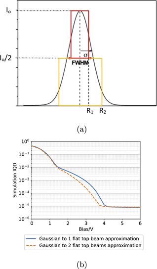
The simulation of the dependence of IQD on bias voltage uses a flat top approximation of the Gaussian laser beam profile as described in section 3.2. This appendix provides an order of magnitude estimate of the introduced error. Better approximation of the experimental Gaussian beam can be made with multiple flat top beams with the same center, different radii and intensities to match the number of photons in the Gaussian beam. Figure A1(a) shows a model with two flat top beams. For conversion of the Gaussian beam with intensity Io and standard deviation σ to two flat top beams, the first flat top beam has the intensity Io/2 and radius R1 =  . The second flat top beam has also the intensity Io/2, whereas the radius is R2 =
  . As seen in figure A1(b), slightly lower IQD is obtained in the range from 1.5 V to 4 V with two flat top beams than with one flat top beam. However, there is no change in IQD at low bias voltages before the corner point and at high voltages with saturated IQD. The deviation between the curves gives an order of magnitude estimate of the error introduced by the flat top approximation. A higher number of flat top beams produces a better approximation of the Gaussian but requires more computer memory and significantly longer simulation time and is currently impractical to do.
Figure A1. (a) Approximation of a Gaussian profile with a combination of two flat top profiles. (b) Simulated IQD of PQED 1 at 647 nm and at optical power of 598 μW with one flat top beam of figure 4 and two flat top beams of (a).
Download figure:
Standard image High-resolution image