

Abstract
This paper presents a detailed assessment of two rectangular metallic waveguide lines in order that they can be used as primary standards to provide metrological traceability for electrical scattering parameter measurements at submillimetre wavelengths. The assessment comprises a series of dimensional measurements to determine the overall quality of the lines in terms of the waveguide aperture size and alignment. This is followed by electrical measurements to confirm the electrical behaviour of the lines. Finally, the lines are employed as standards to calibrate a vector network analyser which is used to measure devices to verify the performance of the lines as calibration standards, in operando. The waveguide size is WM-380, which operates from 500 GHz to 750 GHz.
Export citation and abstract BibTeX RIS

Original content from this work may be used under the terms of the Creative Commons Attribution 4.0 licence. Any further distribution of this work must maintain attribution to the author(s) and the title of the work, journal citation and DOI.
1. Introduction
In recent years, there has been a significant increase in the exploitation of frequencies in the submillimetre-wave range (i.e. from 300 GHz to 3 THz), also referred to as terahertz frequencies, for applications in electronics and telecommunications [1–3], defence and security [4–7], radio astronomy and atmospheric science [8–11], and, healthcare and pharmaceuticals [12, 13]. A recent science and technology roadmap [14] discussed these, and many other, applications.
The most commonly used wave guiding structure for much of this frequency range is rectangular metallic waveguide. Documentary standards have recently been published (i.e. by IEEE [15–17] and IEC [18, 19]) defining the sizes and interconnect mechanisms for these waveguides. This, in turn, has enabled national metrology institutes (NMIs) to use these standardised waveguides to establish metrological traceability at these frequencies (see, for example, [20]). A pre-requisite of such traceability is the availability of suitable artefacts to act as the primary reference standards. Such standards can then be used to calibrate measuring instruments that operate at these frequencies. These days, the most popular, commercially available, measuring instrument for much of this frequency range is the vector network analyser (VNA) which measures signals reflected and/or transmitted by objects (i.e. devices under test (DUTs)). These signals are characterised by the measured scattering parameters (S-parameters) of the DUT.
In order for NMIs to perform reliable S-parameter measurements, the VNA must be calibrated using reference standards. However, these standards must first be characterised and verified as suitable for use in such a role. This paper presents a detailed characterisation and verification of two waveguide lines intended for use as primary reference standards in the WM-380 waveguide band (which is used for frequencies in the range, 500 GHz to 750 GHz) to calibrate a VNA using the so-called '¾-wave' thru-reflect-line (TRL) technique [21]. The characterisation comprises a series of dimensional measurements of the lines' rectangular waveguide apertures and alignment features. This is followed by a series of electrical measurements made using a VNA. The electrical measurements are in two parts: (i) where the lines are measured as DUTs, to help verify the electrical performance of the lines; and (ii) where the lines are used as standards to calibrate a VNA which is used subsequently to measure the electrical characteristics of two verification devices—a long (2'') straight section of waveguide, and, a short (¼-wavelength) cross-connected [22–25] section of waveguide.
The paper is therefore organised as follows: section 2 describes the dimensional measurements used to characterise the lines; section 3 describes the electrical measurements where the lines are used as the DUTs; section 4 provides an analysis of some of the results from sections 2 and 3; section 5 uses the two lines to calibrate a VNA which is then used to make S-parameter measurements of two verification devices. Finally, section 6 presents conclusions from this work. Throughout the paper, the two ¾-wave lines are referred to using their serial numbers: i.e. #11, which has a specified length in [21] of 431 µm; and #22, which has a specified length in [21] of 568 µm. The work in this paper builds on an earlier, preliminary, study into the properties of these types of line as reference standards [26].
2. Dimensional measurements
The dimensional measurements of the two waveguide lines can be divided into three types: (i) waveguide apertures; (ii) interface alignment holes; and (iii) line lengths. The dimensional measurements were made in temperature-controlled laboratories specified at (20 ± 0.1) °C whereas the electrical measurements were made at (23 ± 2) °C. Although there is clearly a difference in temperature for these two measurement conditions, the impact of this temperature difference on the measurements will be negligible for the relatively small sizes of the critical dimensions (i.e. the waveguide apertures and the line lengths). For example, if we assume the lines are made of a material similar to gold, with a thermal coefficient of expansion of 14 × 10−6 K−1, then a temperature change of 5 °C will result in a length of 500 µm increasing by 0.035 µm.
2.1. Waveguide apertures
The apertures of the waveguides were measured using both a scanning white light interferometer and an F25 coordinate measuring machine (CMM). The interferometer was used to assess the overall shape of the rectangular aperture (i.e. the uniformity of the broad wall and narrow wall dimensions), and, to measure the radii of the corners of the apertures. An optical microscope image of the aperture of one of these lines is shown in figure 1. Figure 1(a) shows very good uniformity of both the broad and narrow wall dimensions of this aperture. Both lines showed similar, good, aperture uniformity. This justifies the use of a CMM to measure the aperture using a small number of sampling points. (The ruby ball tip used with this CMM had a diameter of 125 µm. Therefore, due to the small aperture size, there was only room inside the aperture to make measurements at a small number of different locations along the walls of the aperture.)

Figure 1. Optical microscope image of the waveguide aperture of one of the lines: (a) whole aperture; (b) close-up of one of the corners of the aperture. The colour used in these images indicates the relative height of the surface of the face of the interface, close to the waveguide aperture.
Download figure:
Standard image High-resolution imageFigure 1(b) shows that there is detectable rounding of the corners of the aperture. This rounding was characterised in terms of the corner radii, measured using the scanning white light interferometer. The size of each aperture is summarised in terms of the CMM measurements of the broad wall dimension, a, the narrow wall dimension, b, and, the interferometer measurements of the corner radii, R. These measurements are given in table 1. The values of a and b are the mean of five measurement runs. The values of R are the mean values of each aperture's four corners.
Table 1. Measured dimensions of the waveguide apertures of the two lines.
| Line | a (µm) | Δa (µm) | b (µm) | Δb (µm) | R (µm) |
|---|---|---|---|---|---|
| #11 | 382.7 | +2.7 | 190.6 | +0.6 | 18.3 |
| #22 | 381.6 | +1.6 | 190.0 | +0.0 | 19.7 |
The columns Δa and Δb in table 1 indicate the difference between the measured and nominal values for the broad wall dimension (nominal value, 380 µm) and narrow wall dimension (nominal value, 190 µm), respectively. The values for Δa, Δb and R can be used to predict the amount of electromagnetic reflection caused when the lines are connected to a waveguide aperture with perfect dimensions (i.e. a = 380 µm, b = 190 µm, R = 0 µm). Figure 2 shows such a prediction for these lines, which has been computed using CST Microwave Studio electromagnetic simulation software. Figure 2 also shows the combined error due to these three error sources, Δa, Δb and R. The combined error is established using a root-sum-squares combination of the three individual error sources. It should be noted that, for line #22, there is no contribution due to Δb since the measured value of b is the same as the nominal value (to within the uncertainty in the measurement).
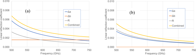
Figure 2. Simulated (linear) reflection coefficient due to errors in aperture dimensions (broad wall, Δa; narrow wall, Δb; corner radii, R): (a) line #11; (b) line #22.
Download figure:
Standard image High-resolution imageFigure 2 shows that, for both lines, the combined reflection due to these errors is less than 0.007 at all frequencies. This suggests that a systematic error of less than 0.007 reflection coefficient will be generated by the apertures of these lines when they are connected to perfect test ports. However, the reflection generated by these apertures, when measured by a VNA, will likely be different from that shown in figure 2, since the VNA test ports will not themselves have perfectly sized apertures. Nevertheless, these plots give some indication of the amount of reflection that these apertures might typically generate when connected to high quality test ports. The values of reflection coefficient shown in figure 2 are less than values given in table 4 of [15]. This is likely due to: different waveguide dimensions used in these calculations (the dimensions used in figure 2 are measured values whereas [15] uses worst-case specified values); different methods used to combine the dimensional errors (in [15], the errors are probably combined as a linear summation, whereas the quadrate summation approach is used here); and, the use of different electromagnetic calculation software ([15] uses QuickWave whereas CST microwave studio is used in this paper)—it is likely that these simulators will use different calculation methods.
2.2. Interface alignment holes
The alignment holes on the interfaces of the two waveguide lines were measured using the CMM. The expanded measurement uncertainty for the dimensions reported in tables 1–5 has been calculated to be 400 nm and is based on a standard uncertainty multiplied by a coverage factor k = 2.18, providing a confidence probability of approximately 95%. The uncertainty evaluations have been carried out in accordance with UKAS requirements (www.ukas.com). The largest contributory term in the uncertainty budget is due to probing error present in the CMM. In the absence of a suitable dimensional reference artefact for the features measured here the magnitude of the probing error was derived from the extreme value of the single-stylus form error, PFTU, MPE, permitted by specification and determined during CMM reverification testing (ISO10360-5:2010). In the absence of experimental data the probability distribution of the uncertainty contributor relating to probing error has been assumed to be rectangular meaning the calculated expanded measurement uncertainty is likely to be pessimistic. There are two types of alignment hole on these waveguide interfaces. These are shown in figure 3. The four outer alignment holes are used in conjunction with dowel pins that form part of the waveguide interfaces found on the measuring instrument (i.e. VNA) test ports to which the lines are connected. The two inner alignment holes can be used, in conjunction with insertable precision dowel pins, to achieve increased alignment accuracy. The diameters and positions for both types of hole, as specified in [16], are listed in table 2. The positions are specified using a Cartesian (x, y) coordinate system relative to an origin defined as the midpoint between the centres of the two inner alignment holes, and, the y-axis is defined as passing through the centres of the two inner alignment holes.
Table 2. Specified values for the inner and outer alignment holes, according to [16].
| Hole type | Nominal diameter (mm) | Tolerance (mm) | Hole number | Nominal position (mm) | |
|---|---|---|---|---|---|
| x-axis | y-axis | ||||
| 4 × outer | 1.702 | +0.025 | 1 | +5.051 | +5.051 |
| −0.000 | 2 | +5.051 | −5.051 | ||
| 3 | −5.051 | −5.051 | |||
| 4 | −5.051 | +5.051 | |||
| 2 × inner | 1.570 | +0.008 | 1 | 0.000 | +3.302 |
| −0.000 | 2 | 0.000 | −3.302 | ||
Table 3. Diameter measurements of the alignment holes.
| Hole type | Line | Measured diameters (mm) | |
|---|---|---|---|
| 4 × outer | #11 | 1.617 | 1.618 |
| 1.617 | 1.617 | ||
| #22 | 1.622 | 1.622 | |
| 1.622 | 1.622 | ||
| 2 × inner | #11 | 1.574 | 1.574 |
| #22 | 1.579 | 1.579 | |
Table 4. Position measurements of the alignment holes.
| Hole type | Hole number | Measured positions (mm) | |||
|---|---|---|---|---|---|
| Line #11 | Line #22 | ||||
| x | y | x | y | ||
| 4 × outer | 1 | +5.058 | +5.057 | +5.057 | +5.056 |
| 2 | +5.057 | −5.057 | +5.057 | −5.057 | |
| 3 | −5.058 | −5.057 | −5.058 | −5.056 | |
| 4 | −5.057 | +5.057 | −5.057 | +5.057 | |
| 2 × inner | 1 | — | +3.306 | — | +3.305 |
| 2 | — | −3.306 | — | −3.305 | |
Table 5. Summaries of the length values (measured and nominal) for the two lines
| Line ID | Nominal length (µm) | Measured length | ||
|---|---|---|---|---|
| Mean | Minimum | Maximum | ||
| (µm) | (µm) | (µm) | ||
| #11 | 431 | 438.3 | 436.8 | 441.3 |
| #22 | 568 | 565.7 | 562.6 | 568.2 |

Figure 3. End view of one of the waveguide lines, showing the four outer and two inner alignment holes, and, the waveguide aperture in the centre. The other four larger diameter holes (that are not labelled) are used to accept the four screws that are used to attach the line to other devices (i.e. in our case, the VNA test ports).
Download figure:
Standard image High-resolution imageIn general, tolerances in the specified diameters of these holes will give rise to random variation (i.e. random error) in electrical measurements of repeated re-connections of these lines. Departures from the specified positions of these holes will give rise to systematic error in electrical measurements made using these lines. Such systematic errors can be investigated by changing the orientation of the line, with respect to the VNA test ports, between repeated connections of these lines. In section 3 of this paper, both these types of connection repeatability (i.e. with, and without, changing the orientation of the line between connection) are investigated during the electrical assessment of each line. However, it is important to recognise that when errors due to waveguide misalignment dominate, statistical bias can be introduced into the electrical results. This has been discussed in [27] and a computer programme to evaluate this effect is available at [28].
The measured diameters of these alignment holes are given in table 3 and the associated position measurements of these alignment holes are given in table 4. The measured diameters of the outer alignment holes given in table 3 are significantly less than the specified diameter value (1.702 mm) given in table 2 (and in [16]). Although this indicates that the interfaces used for these lines are not those specified in [16], these are interfaces currently being used by manufacturers of these waveguides and are therefore indicative of the interfaces currently being used by end-users. This departure from the specified diameter of these outer alignment holes has been observed elsewhere [29], where it has been shown that a smaller diameter for these holes has been chosen by some manufacturers to improve the overall alignment of the waveguide. (The diameter specified by the manufacturer of these lines is 1.613 mm [29].) In fact, [29] shows that the achieved alignment using these smaller diameter alignment holes is comparable with that given in [16], without needing to use the additional inner alignment holes. Values for the maximum (i.e. worst-case) reflection coefficient, for a mated pair of interfaces, caused by the maximum permissible misalignment of the apertures, are given in [16], where −26 dB is the maximum reflection coefficient for this waveguide size. (−26 dB is equivalent to a linear reflection coefficient of 0.05.) This value includes the effects of both random errors due to the tolerances on the diameters of the alignment holes, and, systematic errors due to the positions of the alignment holes.
The diameters of the inner alignment holes in table 3 are within 10 µm of the nominal value given in table 2. However, these holes are not used during the electrical measurements on these lines (discussed in section 3) because these lines have the smaller diameter outer alignment holes which provide acceptable alignment without needing to use additional dowel pins inserted into the inner alignment holes [29].
The measured (x, y) positions of all the alignment holes are within 7 µm of the nominal values given in table 2. The closeness of agreement between measured and nominal values for the positions of these holes suggests that there will not be a significant systematic error when these lines are connected to waveguide test ports conforming to the interface specification given in [16]. In addition, the systematic error due to imperfect aperture size and shape (which was evaluated in section 2.1 and shown to provide an error in reflection of up to 0.007) is considered insignificant compared to the predicted error in reflection of 0.05 (given in [16]) due to the misalignment of the apertures using the interface alignment holes. Therefore, in our case, the main source of error in electrical measurements of these lines is expected to be due to the tolerances on the diameters of the alignment holes thus giving rise to predominantly random errors in the measurements.
2.3. Line lengths
The lengths of the waveguide lines were also measured using the CMM. The mean length of each line was determined from a series of 32 measurement points arranged in a 'star' pattern (as shown in figure 4) established around the central region of the aperture, then calculating the mean z-coordinate of these points. The maximum and minimum z-coordinate values were also recorded. The mean, minimum and maximum lengths for both lines are given in table 5, along with the nominal values (according to [21]) for each length. All measured lengths, for each line, are within a range of less than 6 µm, which indicates that both lines have a uniform thickness over the sampled region. This indicates that the length of each line is a very well-defined quantity. Table 5 also shows that the mean length values are within 8 µm of the nominal values. However, it should be noted that, when these lines are used with the ¾-wave TRL calibration scheme [21], their lengths do not need to be particularly close to the nominal values and so a discrepancy of 8 µm is considered insignificant.

Figure 4. Star pattern (of dots) showing the positions of the 32 measurement points used to determine the length of each waveguide line. The central blue dot shows the position of the waveguide aperture.
Download figure:
Standard image High-resolution image3. Electrical measurements
As mentioned previously, the two lines investigated in this paper were manufactured with smaller diameter outer alignment holes compared with the diameters specified in [16]. According to [29], these smaller diameter alignment holes provide good waveguide aperture alignment without the need to use additional precision dowel pins inserted into the inner alignment holes. Therefore, these inner alignment holes have not been used during the electrical measurements presented in this paper.
3.1. VNA calibration
The two ¾-wave lines under investigation (#11 and #22) are intended to be used as primary standards for calibrating measuring instruments—particularly VNAs. Since part of the evaluation of these lines involves measuring their electrical performance using a VNA, this raises the question; what standards should be used to calibrate the VNA for making measurements of these two lines? It is inappropriate to use the same lines that are being measured as the standards to calibrate the VNA that makes the measurements. This is because this will produce measurements that are not referenced to independent standards—i.e. the measurements will be traceable to themselves and not linked to other (independent) references. Since, in a general sense, measurement implies comparison of quantities [30], a measurement that is referenced to (i.e. compared with) itself is not considered to be a meaningful measurement.
Therefore, to avoid this situation, different standards have been used to calibrate the VNA for making measurements of these two lines. Three separate calibration methods have been used: (i) a short/offset-short/load/thru (SOLT) calibration technique using standards from a commercially available calibration kit [31]; (ii) a TRL calibration technique using a ¼-wave section of waveguide as the line standard; (iii) a second TRL technique using a different ¼-wave line standard. Both TRL line standards have the same nominal length. NPL does not normally use ¼-wave lines as standards at these very high frequencies because such lines are very thin (i.e. of the order of 160 µm) and therefore very fragile.
The reason for using different calibrations is to establish independent sets of measurements for the two ¾-wave lines under investigation—each calibration relies on either a different set of assumptions concerning the properties of the standards used during calibration (in the case of the SOLT and TRL techniques), or, physically different artefacts as the standards (in the case of the two ¼-wave TRL techniques). Figure 5 shows measurements of (a) the reflection coefficient (S11) magnitude, (b) the transmission coefficient (S12) magnitude, and (c) the transmission coefficient (S12) phase, of line #11, measured using the SOLT and the two ¼-wave TRL calibrations (labelled TRL-1 and TRL-2 in figure 5). Since the magnitude of S11 is very small (i.e. less than 0.08) it is not useful to present the measured phase associated with such a small magnitude value (since the inevitable presence of electrical noise will cause the phase to vary dramatically).

Figure 5. S-parameter measurements (using three different calibrations) for line #11. (a) S11 linear magnitude; (b) S12 linear magnitude; (c) S12 phase.
Download figure:
Standard image High-resolution imageFigure 5 shows that there is generally good agreement between the results obtained using the three different calibration techniques. This observation also applies to all the S-parameter results obtained for both lines. The reflection coefficient magnitude results in figure 5(a) show a significant amount of ripple (i.e. rapid oscillation with frequency) on all three sets of results. This is likely to be due to errors that have not been fully corrected by the calibration process and therefore remain present in the measurements as residual errors. There is also considerable ripple on the transmission coefficient magnitude results obtained using the SOLT calibration, in figure 5(b). It is not clear why this ripple is only present in the results using the SOLT calibration—again, post-calibration residual errors are likely to be the cause of this ripple. The results in figure 5(b) obtained using the TRL-1 calibration exhibit a mild resonance at around 560 GHz. This corresponds to an atmospheric absorption line [32, 33] caused by water vapour in the air filling the line. Measurements made around this frequency are generally not considered reliable unless the atmosphere (in terms of the water vapour content) inside the line is tightly controlled. The results for the transmission coefficient phase [in figure 5(c)] show good agreement although there is an unusual step in the results at around 690 GHz. This step is present in many of the phase results and is therefore likely to be a feature of the measurement system hardware (VNA and extender heads) that is not corrected by calibration.
Since there is generally good agreement between results obtained using the three calibrations, henceforth only measurement results obtained from one of these calibrations (i.e. the ¼-wave TRL-1) will be presented.
3.2. Connection repeatability
One indication of good electrical performance for these lines is good connection repeatability. This has been assessed by disconnecting, reconnecting and remeasuring each line, a number of times. For the work presented here, each line was measured four times using this procedure.
An initial assessment of repeatability involved keeping the orientation of each line the same, with respect to the VNA test ports, for each connection. This is so that variability in the measurement results will be due predominantly to the tolerances on the diameters of the alignment holes on the waveguide interfaces of the waveguide lines, and, the alignment holes and dowel pins on the waveguide interfaces on the VNA test ports used during connection. Figure 6(a) shows the results for the four repeatability measurements (labelled R1, R2, R3, R4) of reflection coefficient (S11) magnitude for one of the lines (#11).
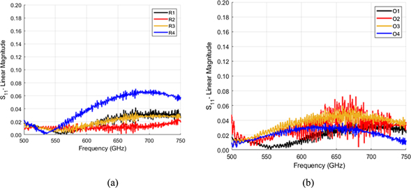
Figure 6. S11 linear magnitude, measurement repeatability for line #11; (a) with no change in orientation between reconnections; (b) with change in orientation of the line between reconnections.
Download figure:
Standard image High-resolution imageA second assessment of repeatability involved changing the orientation of each line with respect to the VNA test ports for each of the four connections. This is so that variability in the measurement results will be due to tolerances on the alignment dowel pins and holes (as before), and, positional errors in these alignment mechanisms and the waveguide aperture, with respect to the VNA test ports. For example, different alignment is likely to be achieved when a line is connected to the same VNA test port, if the line is rotated through 180° prior to re-connection. (The nature of the waveguide interface for this size of waveguide [16] permits two possible orientations for the connection of a waveguide device.) If one of these orientations is called 'up' and the other orientation is called 'down', we can identify four possible connection orientations for a line (i.e. a two-port device) when connected to a two-port VNA:
- (a)Line port 1 connected to VNA port 1—line in 'up' position
- (b)Line port 1 connected to VNA port 1—line in 'down' position
- (c)Line port 1 connected to VNA port 2—line in 'up' position
- (d)Line port 1 connected to VNA port 2—line in 'down' position
Throughout this procedure, port 2 of the line is connected to the other available VNA test port—i.e. VNA port 2, for orientations 1 and 2; VNA port 1, for orientations 3 and 4.
Figure 6(b) shows the results for these four change-in-orientation measurements (labelled O1, O2, O3, O4) for the reflection coefficient (S11) magnitude for line #11.
The connection repeatability measurements (with and without changing the lines' orientation between reconnection) were further analysed in terms of statistical summaries (i.e. standard deviation) as a function of frequency. These statistical summaries give an indication of the variation in the repeated measurements. In general, it was found that there was a similar amount of variation regardless of whether the orientation of the line was changed between reconnections. This can be seen in figure 7 which presents the standard deviations for the repeatability measurements (with and without changing the lines' orientation between re-connections) for both reflection coefficients, S11 and S22, for both lines. This suggests very good positional accuracy for the lines' alignment holes and waveguide apertures. Good positional accuracy was also shown by the dimensional measurements of these holes reported in table 4. The variation seen in figure 7 (in terms of standard deviation) is therefore likely caused by the tolerances on the diameters of the alignment holes on these lines and the alignment holes and pins found on the VNA's test ports. These variations are all less than 0.05 (−26 dB) which, according to [26], is the maximum reflection coefficient expected for this waveguide size due to the maximum permissible misalignment of the apertures for a mated pair of interfaces.

Figure 7. Standard deviation in the measured reflection coefficients for both lines, #11 and #22: (a) with no change in orientation; (b) with change in orientation.
Download figure:
Standard image High-resolution image4. Electrical loss and length
In the previous section, the behaviour of the measured reflection coefficients for these lines were compared with predicted values given in [16] and with the dimensional measurements given in section 2. In this section, the measured transmission coefficients are investigated and compared with other available sources of information. The measured transmission loss is used to calculate the effective resistivity of the conductor of the waveguide lines. This value is then compared with values found in the literature. The measured transmission phase is used to derive estimates of the (electrical) length of the lines, and these values are compared with the dimensional measurements of the lengths of these lines, given in table 5.
4.1. Electrical loss
Reference [15] includes an equation that relates the attenuation constant, α (dB cm−1), of a waveguide to the resistivity, ρ (nΩ.m), of the conductor of a waveguide, assuming classical skin effect and perfectly smooth waveguide walls. This equation is not applicable for thinly plated surfaces for which the plating thickness is less than approximately twice the skin depth.
The equation in [15] is re-arranged to give ρ in terms of α:
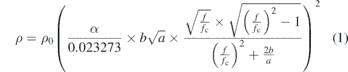
where ρ0 is the reference resistivity (17.241 nΩ.m), a and b (mm) are the waveguide dimensions (a > b), fc (GHz) is the waveguide cut-off frequency, and f (GHz) is the frequency at which the resistivity is calculated. The nominal values of a and b were used in this equation. The value for α, at each frequency, it determined using:

where T (dB) is the measured transmission loss, at each frequency, and l (cm) is the line length. The magnitude (in dB) of either S21 or S12 is used as the value of T at each frequency. The dimensional determinations of each line's mean measured length given in table 5 are used as the value for l for each line.
As an example, figure 8(a) shows the measured transmission loss (as S21 linear magnitude) for the four repeated connections of line #11 (labelled R1, R2, R3, R4). After converting these values to dB, they are used in equation (2) to determine α at each frequency. α is then used in equation (1) to determine ρ at each frequency. Figure 8(b) shows values of ρ derived from the measured loss given in figure 8(a).

Figure 8. Electrical loss for line #11: (a) measured S21 linear magnitude; (b) equivalent conductor resistivity.
Download figure:
Standard image High-resolution imageAs mentioned previously, there is an atmospheric absorption line, due to water vapour, in the spectrum at around 560 GHz. This causes measurements to be unreliable around this frequency. This can be seen in figure 8(a) where the measured S21 becomes greater than one (implying signal gain) at around this frequency. For all other frequencies, the measured S21 is less than one, consistent with a line exhibiting loss. The values of ρ in figure 8(b), relating to line #11, are summarized in terms of the overall mean value (489 nΩ.m), at all frequencies, and the associated standard deviation (333 nΩ.m). Similarly, for line #22, the mean value of ρ was found to be 520 nΩ.m with a standard deviation of 300 nΩ.m.
The mean values of resistivity for both these lines are considerably higher than assumed values for different waveguide materials (i.e. gold, coin silver and copper) given in [15] (which range from 17.1 nΩ.m to 22.0 nΩ.m). The mean values are also considerably higher than an experimentally determined value of resistivity given in [34] (i.e. 28 nΩ.m). However, the standard deviations associated with the two mean values reported here are very large, which indicates that the mean values are not likely to provide reliable determinations of the true values of the resistivity of the lines. The reason these determinations are likely to be unreliable is because the lines are very short and therefore the loss in each line will be close to zero and therefore difficult to detect. Experimental determinations of such low values of loss will be adversely affected by connection repeatability errors (both random and systematic), and the associated non-zero reflection loss, causing the resistivity determinations to be larger than expected (i.e. compared with the values given in [15, 34]) and to vary significantly, as indicated by the large standard deviation values. However, if we assume the true value of resistivity for each line should lie within a range of two standard deviations about the mean value, then the true value of resistivity is expected to be less than 1155 nΩ.m for line #11, and less than 1120 nΩ.m for line #22. This range (albeit somewhat large) does include the values given in [15, 34] and so this provides some degree of assurance that the likely loss in these lines is acceptable.
4.2. Electrical lengths
The measured transmission phase, ϕ, (for either S21 or S12) at each frequency can be used to provide a determination of the 'electrical' length of the line, le, using:

where λg is the guide wavelength at the measurement frequency. Care must be taken, when using this equation, to ensure the value of phase that is used is the absolute phase change. VNAs usually display and record phase on a cyclical (wrapped) scale ranging from −180° to +180°. Values on such a scale need to be 'unwrapped' to ensure there is not an abrupt change in value at the point where there is a dislocation in the phase scale (i.e. at ±180°). In addition, for lines that are longer than one guided wavelength, account must be taken of any whole number of wavelengths that are contained within the line at any given frequency. However, on this occasion, since the lengths of both lines are less than one guided wavelength (i.e. they are ¾-wave lines), there will be no whole number of wavelengths contained within these lines.
As an example, figure 9(a) shows the measured transmission (S21) phase for the four repeated connections of line #11 (labelled R1, R2, R3, R4). These phase values have been 'unwrapped' so that there is not a sudden change in value at around ±180°. The phase values are used in equation (3) to determine le at each frequency. Figure 9(b) shows values of le derived from the measured phase values given in figure 9(a).
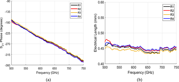
Figure 9. Electrical length for line #11: (a) measured phase of S21; (b) equivalent electrical length.
Download figure:
Standard image High-resolution imageThe values of le in figure 9(b) are summarized in terms of the overall mean value (449.7 µm), at all frequencies, and the associated standard deviation (8.8 µm). The difference between the mean value of le and the dimensionally determined length for line #11 given in table 5 (i.e. 438.3 µm) is 11.4 µm. This difference is within the range of two standard deviations (i.e. ±17.6 µm) and is therefore considered acceptable, in terms of the equivalence between the electrical and dimensional determinations of the length of line #11.
Similarly, for line #22, the mean value of le was found to be 578.3 µm with a standard deviation of 23.7 µm. The difference between the mean value of le and the associated dimensionally determined length given in table 5 (i.e. 565.7 µm) is 12.6 µm. Once again, this difference is within the range of two standard deviations (i.e. ±47.4 µm) and is therefore considered acceptable. Hence, the electrical and dimensional determinations of length for line #22 are considered equivalent.
5. DUT measurements
Having demonstrated the suitability of these two lines as standards for calibrating a VNA using the ¾-wave TRL technique [21], it is informative to perform such a calibration and then measure some devices to demonstrate the overall performance of the calibrated measurement system. Two devices have been chosen for this purpose. The behaviour of both devices can be predicted, to some extent, using other information. The predicted performance is used to verify the measurements made by, and hence the calibration of, the VNA. The devices are:
- (a)A 2'' section of straight waveguide. As with the electrical measurements of the ¾-wave lines, described in section 4, the measured transmission loss for this 2'' section can be used to determine the resistivity of the conductor of the waveguide. The resistivity can then be compared with values found elsewhere ([15, 34]). The measured transmission phase can be used to determine the electrical length of the line. The electrical length can then be compared with a dimensional determination of the length of the line.
- (b)A short (¼-wave) section of cross-connected waveguide. The measured transmission loss (in dB) for this type of waveguide can be compared with values produced using electromagnetic simulation software (CST Microwave Studio). Cross-connected waveguides have very high reflection loss (i.e. linear magnitudes close to unity) and transmission loss that depends on the length of the cross-connected waveguide [22–25].
The ¾-wave TRL calibration technique uses both ¾-wave lines simultaneously to provide the line standard information during the calibration. The usefulness of the information provided by the lines depends on the transmission phase change provided by each line at each frequency. Therefore, a selection process is employed that weights the information for each line at each frequency, based on the line's phase change. This process is described in detail in [21] and so will not be repeated here. These lines provide optimum information when their phase change is 270° (i.e. at ¾ of a wavelength). However, information can still be used, suitably weighted, at other values of phase change.
Figures 10 and 11 show results obtained for the 2'' section of waveguide, and figure 12 shows results for the cross-connected waveguide. Figure 10(a) shows the measured transmission loss (linear magnitude) for the 2'' waveguide section, and figure 10(b) shows the associated resistivity of the waveguide conductor, derived from the measured transmission loss [using equations (1) and (2)]. The average value of resistivity, averaged over frequency, is 27.9 nΩ.m with an associated standard deviation of 3.4 nΩ.m. This value is higher than values given for different low loss metallic conductors given in [15] (which range from 17.1 nΩ.m to 22.0 nΩ.m). However, the values in [15] relate to bulk metals, which are expected to have lower resistivity compared with metals which have been machined during manufacturing processes (as is the case with these waveguide lines). The resistivity for the 2'' line agrees very well with an experimentally determined value of resistivity found in [34] (i.e. 28 nΩ.m) , where the transmission loss of several lines of differing lengths (ranging from 1'' to 5'') were measured and a similar calculation was used to determine the equivalent conductor resistivity.
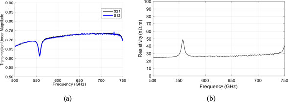
Figure 10. 2'' section of straight waveguide: (a) measured transmission, linear magnitude; (b) equivalent conductor resistivity.
Download figure:
Standard image High-resolution image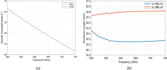
Figure 11. 2'' section of straight waveguide: (a) measured absolute unwrapped transmission phase; (b) equivalent electrical length.
Download figure:
Standard image High-resolution image
Figure 12. ¼-wave section of cross-connected waveguide: measured and modelled transmission coefficient magnitude (dB). Three modelled curves are shown, relating to the b dimension: (i) nominal value; (ii) nominal value +3.8 μm (+delta); (iii) nominal value −3.8 μm (− delta).
Download figure:
Standard image High-resolution image
Figure 11(a) shows the measured transmission phase for the 2'' waveguide section, and figure 11(b) shows the associated electrical length derived from the measured transmission phase (i.e. the trace labelled 'a = 380 µm'). The phase values in figure 11(a) represent the absolute phase after unwrapping the values measured by the VNA, which are recorded on a scale ranging from −180° to +180°. The absolute phase change is very large—i.e. ranging from −18.6 k° (i.e. −18 600°) to −38.5 k°—due to the relatively long length of this line (i.e. approximately 50.8 mm) compared with the guide wavelength (which varies from approximately 1.0 mm to 0.5 mm across this waveguide band). The electrical length labelled '380 µm' in figure 11(b) shows a dependence with frequency, which is not expected. In addition, the average value of electrical length, averaged over frequency, is 50.277 mm with an associated standard deviation of 0.047 mm, whereas a dimensional determination of the length of this line, made using a digital calliper, was found to be 50.80 mm, which is considerably more (i.e. by 0.52 mm) than the average electrical length. However, the calculation of electrical length assumes nominal values for the dimensions of the waveguide aperture. Using a different value for the aperture dimensions (specifically, the broad wall dimension) will cause the calculated electrical length to change. For example, the trace labelled 'a = 388 µm' in figure 11(b) corresponds to an assumed broad wall dimension of 388 µm, which is within the expected tolerance (i.e. 10 µm) for this dimension of this waveguide. (It is not possible to measure the broad wall dimension of this waveguide since much of the length is inaccessible, since it is a very small internal dimension.) The curve labelled 'a = 388 µm' in figure 11(b) shows much less variation with frequency, compared with the curve labelled 'a = 380 µm'. In addition, the average of these electrical length values is 50.792 mm, with a standard deviation of 0.075 mm. This average value is much closer to the dimensional determination of length (i.e. a difference of 0.008 mm, which is well within one standard deviation of the mean electrical length). This shows that the level of agreement between the electrical and dimensional determinations of the length of this line is acceptable, considering only partial knowledge is available concerning the likely broad wall dimension of this 2'' section of waveguide.
Figure 12 shows the measured and modelled transmission coefficient (in dB) for the ¼-wave section of cross-connected waveguide. The transmission coefficient for a cross-connected waveguide is strongly related to the width of the narrow wall dimension, b, of the waveguide aperture, as discussed in [24]. Therefore, figure 12 includes three sets of modelled values: (i) assuming the nominal value for b (190 µm); (ii) assuming that b is oversized by 3.8 µm (i.e. 193.8 µm); (iii) assuming that b is undersized by 3.8 µm (i.e. 186.2 µm). The change in b of ±3.8 µm (labelled 'delta' in figure 12) corresponds to one of the tolerances used to specify waveguide grades given in [15]. Generally, there is good agreement between the measured and modelled values. The difference between the measured and modelled values (assuming the nominal value for b), at all frequencies, is less than 2 dB, which is within the range of modelled values indicated by the ± delta (3.8 µm) tolerance interval for b shown in figure 12.
The good agreement, shown in figures 10–12, between measurement-derived values and the predicted values confirms that the calibration of the VNA has been successful and therefore the two ¾-wave lines (#11 and #22) investigated in this paper are suitable as standards for such calibrations. A more detailed validation of the overall calibrated measurement system would need to include knowledge concerning the uncertainty in the S-parameter measurements. However, this is beyond the scope of this paper and will be addressed during future investigations into the uncertainty achieved by this measurement system.
6. Conclusion
This paper has presented a comprehensive evaluation of two waveguide lines intended for use as primary standards for scattering parameter measurements at submillimetre-wave frequencies (specifically, in waveguide WM-380, which operates from 500 GHz to 750 GHz). A series of dimensional measurements were made to characterise the size of the waveguide aperture and the interface alignment holes for both lines. The dimensions of the apertures of the waveguides were found to be within 3 µm of the nominal values. The positions of the alignment holes were found to be within 7 µm of their nominal values. These dimensional measurements were used to predict the electrical behaviour of the lines, in terms of their likely mismatch when connected to the test ports of a VNA during calibration. Dimensional measurements were also used to determine the lengths of the two lines. This involved making a series of measurements in the vicinity of the waveguide aperture to evaluate the flatness of the surfaces of the lines.
A series of electrical S-parameter measurements were then made on the lines to check the reflection and transmission properties of the lines, in operando. The lines' reflection coefficients were found to be less than 0.1 (linear magnitude). Connection repeatability measurements were also performed as part of these electrical measurements. The measurements of transmission loss were converted to the effective resistivity of the waveguide conductor so that these values could be compared with values found elsewhere (e.g. in the literature [15, 34]). The measurements of transmission phase were converted to electrical length so that these values could be compared with the dimensional length determinations.
Finally, the two lines were used to perform a ¾-wave TRL calibration [21] of a VNA which was used subsequently to measure two DUTs—a 2'' section of straight waveguide and a ¼-wave section of cross-connected waveguide. The results for both these DUTs showed good agreement with values predicted by other means—i.e. the effective resistivity and electrical length of the 2'' straight waveguide, and, the modelled attenuation for the cross-connected waveguide. For example, for the 2'' straight waveguide, the measured conductor resistivity was found to be 27.9 nΩ.m, with a standard deviation of 3.4 nΩ.m, compared with a published value of 28 nΩ.m for similar such lines. The measured line length was found to be 50.792 mm, with a standard deviation of 0.075 mm, compared with a dimensionally determined value of 50.80 mm.
The conclusion from this investigation is that these two lines are considered suitable as primary reference standards for scattering parameter measurements in the WM-380 waveguide size, at all frequencies ranging from 500 GHz to 750 GHz. As a result of this investigation, these lines will now be used as the UK's primary national standards for these measurements and will form the basis of a detailed uncertainty analysis that will be undertaken as part of the overall characterisation of the complete measurement system.
Acknowledgments
The work described in this paper was partially funded and supported by the research project 18SIB09 TEMMT (Traceability for electrical measurements at millimetre-wave and terahertz frequencies for communications and electronics technologies) sponsored by the European Metrology Programme for Innovation and Research (EMPIR). The EMPIR initiative is co-funded by the European Union's Horizon 2020 research and innovation programme and the EMPIR Participating States. It was also partially funded and supported as a cross-theme project in the 2020-2021 National Measurement System (NMS) Programme of the UK Government's Department for Business, Energy and Industrial Strategy (BEIS). The authors thank Dr Jeffrey Hesler, VDI, for the loan of the two ¼-wave lines that were used in this paper, for (i) some of the VNA calibration standards that enabled S-parameter measurements to be made of the two ¾-wave lines, and (ii) the section of cross-connected waveguide. The authors also thank SWISSto12 for supplying the lines used in this paper.