Abstract
Granular power management in a power-efficient system on a chip (SoC) requires multiple integrated voltage regulators with a small area, process scalability, and low supply voltage. Conventional on-chip analog low-dropout regulators (ALDOs) can hardly meet these requirements, while digital LDOs (DLDOs) are good alternatives. However, the conventional DLDO, with synchronous control, has inherently slow transient response limited by the power-speed trade-off. Meanwhile, it has a poor power supply rejection (PSR), because the fully turned-on power switches in DLDO are vulnerable to power supply ripples. In this comparative study on DLDOs, first, we compare the pros and cons between ALDO and DLDO in general. Then, we summarize the recent DLDO advanced techniques for fast transient response and PSR enhancement. Finally, we discuss the design trends and possible directions of DLDO.
Export citation and abstract BibTeX RIS
1. Introduction
Resources in system-on-a-chip (SoC) are highly dynamic. Fig. 1 shows, under different workloads, resources such as execution units (EUs), fixed functions (FFs), and media units that can be in high demand, low demand, or retention modes. Therefore, for good system energy efficiency, we should use individual supply voltage domains for these units, each with a voltage regulator, a. k. a. granular power management[1, 2]. Candidates for the regulator are the DC–DC converter and the low-dropout regulator (LDO). Although LDO suffers from an inherently lower efficiency than that of the DC–DC converter (100% in an ideal case), it is more compact with the removal of large energy storage components (inductors, capacitors) and hence suitable to obtain a fully-integrated voltage regulator (FIVR) in an SoC. Besides, a fully-integrated LDO reacts swiftly to the load transients for its light-weight nature (with a single-pole power stage).
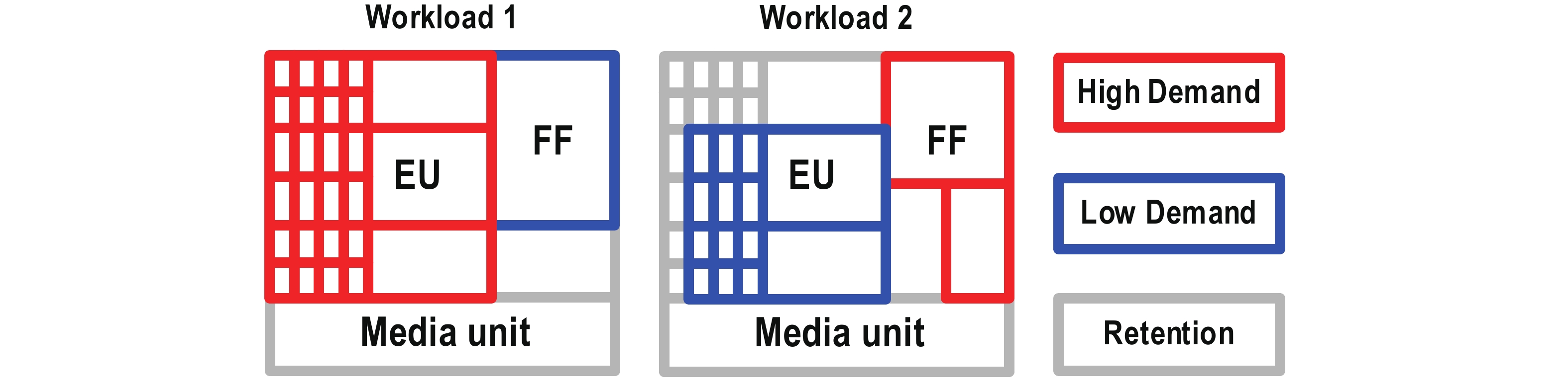
Fig. 1 (Color online) Granular power management in an SoC.
Download figure:
Standard imageHowever, for an energy-efficient SoC, the load circuits may operate at a near-threshold supply voltage like 0.5 V, while the dropout voltage should be small, for example 50 mV. These working conditions hardly suit analog LDOs (ALDOs)[3–9], which need sufficient voltage headroom to realize a high loop gain to minimize the steady-state error of the output voltage. Alternatively, we may use the multistage topologies to increase the loop gain, but complicated frequency compensation techniques are then necessary.
On the other hand, digital LDOs (DLDO) are a good alternative[10–41] for a power-efficient SoC. The digitized power transistors of the DLDO work like switches, allowing a small dropout voltage (Fig. 2). Also, we can easily implement a high loop gain with a digital integrator that is not limited by the minimum supply voltage (VMIN).

Fig. 2 (Color online) DLDO requirements in an SoC.
Download figure:
Standard imageThe widely-adopted shift-register-based DLDO firstly proposed in Ref. [10], included a power switch array, a clocked comparator to sense the output and the reference voltage difference, plus a shift-register (acting as an integrator) to generate a control word of the power switch array. Yet the synchronized shift-register only changes the control word by 1-bit every clock cycle, and thus only a high-frequency clock will allow a fast response. This increases the power consumption of the synchronized circuits. To address this trade-off, many techniques have been proposed, they will be addressed and discussed in this paper.
Another issue faced by DLDO is the power supply rejection (PSR). Fig. 2 illustrates how the load current change from a neighbor load may cause voltage ripple on the shared DLDO input. Also, input ripple can come from the pre-stage DC–DC converter. Unfortunately, the PSR of the DLDO is inherently inferior to that of the ALDO, especially when we maintain the control clock as low under the power consumption constraint. As a result, significant ripples may also occur at the DLDO output node. To prevent abnormal/interrupt operations of the load circuits caused by these supply ripples, implies the addition of a margin above the minimum workable supply voltage VMIN, which undermines the efficiency. Therefore, this paper will also investigate PSR enhancing techniques for DLDO[32–35].
This paper has the following organization: Section 2 discusses the pros and cons of the ALDO and the DLDO. Section 3 reviews the DLDO techniques on how to minimize output voltage spike, recovery time, and improve PSR. Section 4 presents the possible future trends of the DLDO design, and draws the conclusion.
2. Comparison between analog and digital LDOs
2.1. Low voltage operation and process scalability
Fig. 3 presents the basic block diagrams of the ALDO and the DLDO. The ALDO compares the output voltage (VOUT) with the reference voltage (VREF) through an error amplifier (EA). The EA's output feeds a power transistor that operates in the saturation region in most of the cases, although it sometimes operates in the linear region as well. To maintain good output accuracy, the ALDO should have an EA with sufficient loop gain. To circumvent the stability issue of a multistage system, it would be necessary to have a one- or two-stage EA with cascode devices. Yet, more cascode devices stacked imply a larger voltage headroom, which limits the minimum supply voltage of an energy-efficient SoC. Moreover, the analog EA has a weak process scalability, and requires re-design in process migration.

Fig. 3 Block diagram of (a) ALDO and (b) DLDO.
Download figure:
Standard imageThe DLDO replaces the analog EA by a VOUT sensor and a controller (integrator) implemented with digital circuits. The digital integrator manages to provide a very high DC gain that is irrelavent to its supply voltage, breaking the trade-off between loop gain and supply voltage in the analog design. As such, DLDO works well with a low supply voltage, and scales naturally with an advanced process. Meanwhile, the switch operation of the power transistors conducts more current with a full turn-on voltage (VDD), saving silicon area.
In recent years, the inverter-based LDO[42–44] stems from the ring amplifier, for low-voltage operation. They achieve a fast response with the inverters working in an analog fashion. However, to reduce shoot-through currents in the inverters, offset voltages should exist for proper biasing. Obviously, during process migration, the offset voltages require a dedicated calibration circuit, otherwise, re-design is necessary.
2.2. Power-speed trade-off
The widely adopted figure of merit (FoM) of speed proposed in Ref. [45] explains the power-speed trade-off of LDO:

where TR is the transient response time, IQ is the quiescent current, IMAX is the maximum load current, COUT is output capacitor, and ΔVOUT is the output voltage spike with the IMAX load step.
For an ALDO, TR is mainly determined by the bandwidth of the LDO loop and slew rate, which should be inversely proportional to the IQ. Multiple-loop schemes could be a good way to reduce TR without significantly increasing IQ [4, 46].
The synchronous DLDO should have a longer TR and thus a slower transient response under the IQ constraint, due to the conventionally discrete VOUT sampling and synchronized control word changing, as illustrated in Fig. 4. When a load current (ILOAD) step comes at t1, DLDO fails to respond instantly. The output capacitor compensates the difference between ILOAD and LDO output current ILDO, leading to a VOUT drop, until the next clock (CLK) rising edge (t2) when the synchronized comparator can respond. To prevent metastability, the controller, lagging one-cycle behind t2 (t3), processes the comparator's output (CMPOUT). After that, the control word n begins to increase, providing additional current ILDO. We define ΔtD = t3 − t1 as the loop delay, and VOUT the undershoot caused by ΔtD is ΔVDLY. Subsequently, VOUT does not stop decreasing until ILDO = ILOAD, depending on how fast the controller can find the desired control word within the processing time (ΔtP). This adds an additional voltage drop ΔVREACT to the overall undershoot ΔVMAX = ΔVDLY + ΔVREACT. Consequently, the TR of the DLDO consists of ΔtD and ΔtP, where only ΔtP contributes to the TR in analog counterparts.

Fig. 4 (Color online) The output voltage undershoot analysis of DLDO.
Download figure:
Standard imageDue to the discrete sampling, the maximum ΔtD is two-clock cycle. Hence under the power consumption constraint, ΔVDLY of the DLDO would be larger than that of the ALDO. To reduce ΔtD, continuous or asynchronous sampling techniques emerged, presented next in Section 3.
To reduce ΔVREACT, many recent DLDO techniques tried to find out the desired control word within a few cycles, taking the advantage of digital operations (discussed in Section 4). This imposes the DLDO to have a comparable or even smaller ΔVREACT than the ALDO.
2.3. Stability and limit cycle oscillation
For conventional ALDO designs, an ALDO will become unstable or even oscillate once its phase margin is not enough. But regarding the DLDO, which typically has a DC pole from the digital integrator, large signal unstable behaviour is less likely to happen. However, DLDOs suffer from another oscillation phenomenon inhexistent in ALDOs. Because of the digitized output current with limited resolution, there will always be a quantization error in the DLDO, inciting a limit cycle oscillation (LCO).
The quantization level determines the quantization error. Fig. 5(a) displays a measured VOUT LCO waveform of a two-level quantized DLDO[11], with a period of integer clock cycles and an amplitude of several milli-volt. Refs. [12, 13] explain the difference between an LCO and oscillation in analog circuits, with the small-signal model of a two-level quantized DLDO in Fig. 5(b). With a DC pole and an output pole, Fig. 5(c) plots the root locus of this system. The LCO appears when the root locus crosses the unit circle (a "healthy" oscillation). By contrast, the analog loop instability basically occurs outside the unit circle. Ref. [11] further investigated a method to predict the period and amplitude of the LCO.

Fig. 5 (a) Measured LCO of DLDO, (b) small-signal model of DLDO, and (c) root locus of 2-level quantized DLDO.
Download figure:
Standard imageGenerally speaking, a smaller least significant bit (LSB) current reduces the quantization error and subsequently the LCO. Nonetheless, the small LSB exponentially increases the control bits required for the targeted output current. A pulse-width-modulated (PWM) LSB scheme proposed in Ref. [14] reduces the effective LSB. Additionally, Ref. [11] added an auxiliary path to reduce the LCO mode to 1 across a wide load current range.
2.4. Power supply rejection
An ALDO can achieve a good PSR with a properly designed EA and a dominant pole allocation[4, 9], or by adding a feedforward path to cancel the supply input ripple[7]. But the low supply and dropout voltages in an energy-efficient SoC inevitably undermine the achievable PSR.
Fig. 6 illustrates the power supply ripple rejection process of a DLDO, where discontinuous sampling and control word changing will excite significant glitches with a supply voltage ripple. We define the optimum control word n (nopt) that imposes VOUT = VREF in the steady-state, with the change of n synchronized with the clock rising edge. In an ideal case, the controller manages to find out nopt (n1 = nopt) at each sampling point (t0, t1, t2, t3), with VOUT pulled-back to VREF. However, during the sampling intervals, e.g., from t0 to t1, with n fixed, the instant PSR becomes:

Fig. 6 (Color online) Power supply rejection process of a conventional DLDO.
Download figure:
Standard image

where rds represents the instance resistance of the power transistor (constant value during the intervals), RLOAD is the load resistance. This indicates that the DLDO is vulnerable to the supply ripple during the sampling intervals.
For the non-ideal cases when n1 ≠ nopt, e.g., at t1, it causes an error Ve = VOUT − VREF. Then before the next sampling, VOUT starts to increase with VIN from Ve, leading to a larger VOUT ripple. Therefore, the only way for a conventional DLDO to improve the PSR is to minimize the sampling interval using a faster CLK. Unfortunately, this contradicts the power-efficient prerequisite. Section 5 introduces several techniques to incorporate a continuous analog path to enhance the PSR.
3. Design considerations about the DLDO
3.1. Quantizer
A quantizer will approximate the voltage error between VOUT and VREF for further processing. Conventional DLDOs use a two-level, synchronized, latch-based comparator[2, 10, 13, 15–18], as shown in Fig. 7, quantizing VOUT to a binary output. The complementary clock-controlled switches in the comparator eliminate the steady quiescent current. However, the clock limits the quantization speed, and the discontinuous sampling causes a certain delay ΔtD. Meanwhile, the unbalanced parasitic capacitance and transistor mismatches will cause input offset[19].

Fig. 7 Latch-based comparator.
Download figure:
Standard imageHigh-performance DLDO designs[20–23] use continuous quantization, typically achieved with a multi-level quantization (functioning as an analog-to-digital converter, ADC). In Ref. [21], a transconductance stage continuously compares VOUT and VREF, and a current-to-code converter generates a multi-bit output (Fig. 8(a)). A code-dependent reference increases the dynamic range and resolution of the converter. Ref. [22] designed a continuous quantizer also based on inverters, as shown in Fig. 8(b). An auto-zero technique removes the input offset voltage of the aforementioned inverter-based analog LDO. A time-to-digital converter (TDC) is another candidate for continuous multi-level quantization[23], but needs calibration on the delay time. Plus, the quantized multi-level signals processed by digital logic lead to a more coherent DLDO. But in general, the power consumption of the multi-level quantizer is much higher.

Fig. 8 Continuous multi-bit quantizer based on (a) current-mirror and (b) inverter.
Download figure:
Standard imageA voltage-controlled oscillator (VCO) can also be a continuous quantizer[24, 25]. Fig. 9 shows how with the two VCOs driven by VOUT and VREF, the DLDO system looks like a phase-locked loop (PLL). In the steady-state, the VCOs should oscillate at the same frequency, resulting in a fixed phase error subsequently converted to a control word by the phase detector (PD). When a load current step occurs, the VOUT spike information turns into an incremental phase error, captured by the PD and processed by the controller. The main drawback of this topology is that the VCO is essentially an integrator (1/s), that needs enhancement of the transient speed by a proportional control, as presented next.

Fig. 9 DLDO based on a VCO quantizer.
Download figure:
Standard imageAs a brief summary, the features of the quantizers in DLDO design are included in Table 1.
3.2. PID control
One of the possible solutions to address the power-speed trade-off of the DLDO is to use asynchronous control logic[26, 27], but the asynchronous design may not be robust under process, voltage, temperature (PVT) variations.
Another straightforward way combines the proportional, integral (PI), and even derivative (PID) controls[28] for better transient response. Fig. 10 displays the conceptual transient waveforms of these controls. For a conventional I-control that has a large DC gain, DLDO achieves an accurate steady-state output but low speed. By contrast, P-control can minimize VOUT undershoot, but lacks the capability of reducing the steady-state error. PI-control can address both drawbacks, while PID-control further suppresses the recovery overshoot.

Fig. 10 (Color online) Output voltage transient response under I-only, P-only, PI, and PID control.
Download figure:
Standard image3.2.1. Digital PID control
As discussed above, the number of the quantization levels should be proportional to the power consumption. For a low power design, the detection of whether VOUT exceeds the VREF window[2, 13] can activate the P-control, namely a three-level quantization. Fig. 11 presents the comparison of VOUT in two comparators, with VREFH and VREFL, respectively, forming a VREFH −VREFL window. When VOUT exceeds this window, the sampling frequency increases with P-control, driving VOUT back to the window quickly. When it is within the window, the comparison of VOUT with VREF generates the control word after the integrator, as an I-control.

Fig. 11 Change CLK when VOUT exceeds the VREF window.
Download figure:
Standard imageHigh-performance designs employ typically a multi-level quantization with an ADC[14, 20–22]. With the VOUT information converted to the digital domain, the control circuits can perform easily the PID control. However, to reduce the loop delay, a power-hungry ADC may be necessary.
Granular power management oversees not only the VOUT overshoot/undershoot, but also the recovery time. For a linear increment control used in the conventional DLDO[10], the control word can only change one count per clock cycle, resulting in a very long recovery time. The coarse-fine tuning scheme used in Refs. [2, 13, 29], changes the control word in multiple counts per clock cycle (coarse-tuning) once VOUT exceeds the predefined window. A more aggressive scheme utilizes binary search with the control word changing with 2N [14], with D-control added to prevent a recovery overshoot. To reduce the overshoot without D-control, Ref. [30] used exponential control expressed as:

where the recovery time may be a bit longer than the binary search.
3.2.2. Analog-assisted loop
By using analog circuits to sense VOUT [15–18, 31] as the fast loop can also be a candidate, due to the continuous nature of the analog circuits. Meanwhile, it is worthwhile to utilize passive devices, as active circuits may still have limitations in terms of their low supply voltage and small dropout.
Fig. 12(a) presents an "analog-assisted" method proposed in Refs. [15, 16]. A passive high-pass network RC and CC couples to the ground of the driving inverters (VSSB) the high-frequency components of VOUT. RC biases VSSB to the ground in the steady-state, while drops to a negative value (almost equal to the VOUT undershoot) at the load transient with a minor delay, allowing the power transistors to generate more instantaneous output current as a high-pass path. Ref. [17] further reduces the VOUT undershoot by providing more instantaneous current, through coupling VOUT to the body of the power transistors. The drawback of these schemes is that the analog circuit can only assist the turned-on power transistors, setting a limit on the minimum output current. Ref. [18] proposed an improved version (Fig. 12(b)), where analog paths include not only the high-pass network (P2), but also NMOS pass devices (P1). This advances the PMOS counterpart, by providing more instantaneous current from both turned-on and -off pass devices. Nevertheless, this benefit trades with the need for a gate drive voltage higher than the supply voltage. Ref. [31], although not implemented from a digitized output power transistor array, also utilizes a capacitor to couple the output spike to the gate of the power transistor as a high-pass path (Fig. 12(c)). A charge pump generates the gate voltage of the power transistor. Though it is analog in nature, it can be a good candidate for a low-power DLDO.

Download figure:
Standard imageIn addition, the analog-assisted methods can be an effective solution to improve the DLDO transient response without using advanced process. Table 2 summarizes the process nodes and FoMs (from (1)) of state-of-the-art DLDO works, to evaluate how the process advancement enhances the DLDO performance. As can be seen, the FoM value decreases with process scaling down for the ADC-based DLDO designs[21, 22, 36, 39, 40]. This stems from the fact that the ADC and digital processing has a higher speed and better power efficiency with advanced process. Yet, it is interesting to find out that the analog-assisted-based DLDOs[15, 18] manage to achieve even better FoMs with a cost-effective process, which is facilitated by the continuous response of the analog circuits.
3.3. PSR improvements
As discussed in Section 2, the DLDO has inherently mediocre PSR even when the optimum control word can be found. Instead, analog circuits may be the only solution under the power consumption constraint. As illustrated in Fig. 13(a), by parallelizing an analog resistance rds,A with the digitized resistance rds,D, the overall resistance can change continuously. Additionally, feedback loops may adjust rds,A from the supply voltage noise, just like in the ALDO. Then, with the supply voltage VIN-to-VOUT response mainly determined by the analog circuits, they allow a longer digital sampling interval (t4 to t5), and thus higher power consumption. Fig. 13(b) exhibits a topology that combines analog and digitized resistance classified as an hybrid LDO[32].

Fig. 13 (a) Analog circuits help PSR improvement and (b) block diagram of the hybrid LDO.
Download figure:
Standard imageAlthough the working principle of the PSR improving techniques in the digital/hybrid LDO are similar to those in the ALDO, there are two critical issues remaining. Firstly, we expect the current provided by the analog part to be small. Hence even with a continuously adjustable rds,A, this LDO fails to respond to a large supply ripple. Secondly, the limited supply voltage and dropout undermine the achievable PSR of the analog circuits.
Ref. [33] employed one ALDO array and one DLDO array, and proposed a feedforward PSR cancellation technique (Fig. 14(a)), implemented with a resistor and capacitor between the supply voltage and the gate node of the power transistor. It improves the light-load PSR, degraded at heavy load. To maintain the PSR performance, the architecture should comprise more ALDOs and less DLDOs under heavy load conditions.
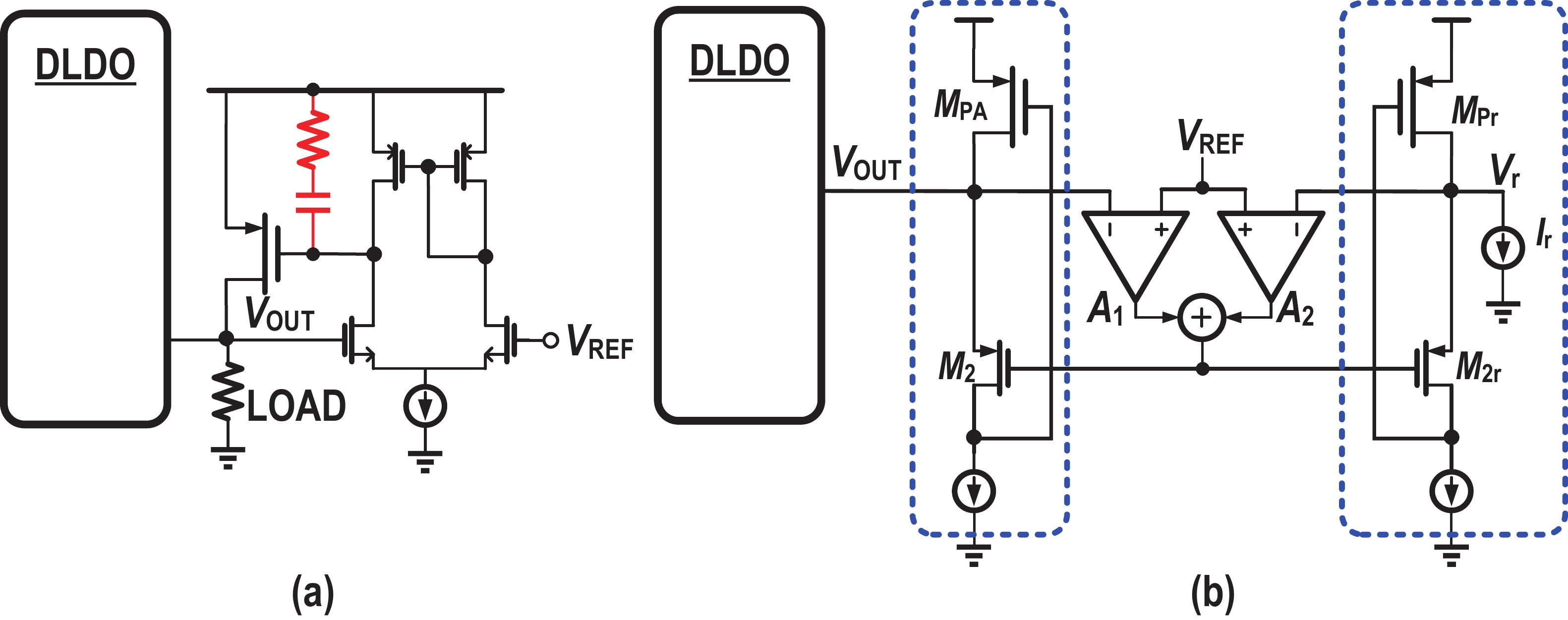
Download figure:
Standard imageAs presented in Fig. 14 (b), Refs. [34, 35] added an active replica loop to enhance the PSR. The main part of the ALDO constructed from a flipped voltage follower (FVF)[4, 5] (MPA, M2, A1), manages to work under a low supply voltage with a fast transient response. Fig. 15 plots the simulated PSR, showing a significant improvement above 10 kHz, when compared with a conventional DLDO. The addition of the replica loop, composed by MPr, M2r, and A2, increases the loop gain and then improves the PSR by 6 dB (5.3 in simulation). Additionally, the current provided by the ALDO dynamically increases with heavy load PSR. However, the utilization of many analog circuits obviously undermines the process scalability.

Fig. 15 (Color online) Simulated PSRs of the conventional DLDO, hybrid LDOs without replica loop, and with replica loop.
Download figure:
Standard image4. Discussion and conclusion
With the development of efficient computing and granular power management techniques, the DLDO has drawn significant attention in recent years. When compared with its analog counterpart, the DLDO suits well the requirements of low voltage operation and process scalability. However, inferior performances in the transient response, recovery, and PSR prevent its further application. Previous works proposed partially address these issues. Alternatively, analog techniques complementary to the DLDO can improve the transient response and the PSR. Yet, the achieved PSR so far is still too low to supply analog or RF circuits.
For the future design trends, it would not be easy for the DLDO to achieve a similar or even better performance than the ALDO, at circuit level. Instead, the performance should be significantly improved in the digital domain, or at the system-level. For instance, to maintain the stability and fast response, the PID coefficients were dynamically set in Ref. [39] through a digital calibration algorithm. Meanwhile, Ref. [40] proposed a computational scheme to determine the duration of the fully turn-on/turn-off power transistor array, for a very fast transient response. It would be possible to incorporate machine-learning techniques to predict, study, and respond to the load and supply changes. Moreover, fully synthesizable DLDOs[36–38] are attractive with perfect compatibility to digital design flow and process scalability. Finally, it is interesting to investigate high current DLDOs with distributed layout and current sharing function. For instance, consider that some DLDOs in an SoC might not provide full load current in most workload scenarios, it is reasonable to make them to assist neighboring load steps[41], as shown in Fig. 16. How to equalize the assisting currents may worth further studying.

Fig. 16 (Color online) Multi-LDOs assisting a neighboring load step.
Download figure:
Standard imageAcknowledgements
This work was supported by the National Natural Science Foundation of China (No. 61974046), the Provincial Key Research and Development Program of Guangdong (2019B010140002), the Macao Science & Technology Development Fund (FDCT) 145/2019/A3 and SKL-AMSV(UM)-2020-2022.