Abstract
Thin films of CdS have been prepared by chemical spray pyrolysis by spraying precursor solution directly onto soda lime glass (SLG) substrates. Influence of substrate temperature on structural, optical, morphological and electrical properties have been investigated by using various techniques such as low angle X-ray diffraction (XRD), Raman spectroscopy, X-ray photoelectron spectroscopy (XPS), field emission scanning electron microscopy (FESEM), atomic force microscopy (AFM), transmission electron microscopy (TEM), UV–visible spectroscopy photoluminescence (PL) spectroscopy etc. Formation of CdS has been confirmed by low angle XRD, Raman spectroscopy and XPS analysis. XRD pattern showed that CdS films are polycrystalline, have hexagonal structure and prefer orientation of crystallites shifts from (101) to (002) with increase in substrate temperature. Raman spectroscopy revealed that exciton-phonon coupling depends on substrate temperature and hence on crystallite size. Optical band gap increased from 2.43 to 2.99 eV when substrate temperature increased from 325 to  . Transmittance of the film also showed an increasing trend from
  to
to  with increase in substrate temperature. Such high band gap and transmittance values of CdS films prepared at
  make it a useful window material in CdS/CdTe and CdS/Cu2S heterojunction solar cells.
Export citation and abstract BibTeX RIS
1. Introduction
In terms of both fundamental and applied research, the synthesis and characterization of semiconductor nanocrystals are of significant interest in the light of their tunable electronic, optical and catalytic properties which subsequently occur from the size confinement effect. In this direction, metal chalcogenides like sulfides, selenides and tellurides, especially those belonging to II–VI compound group are of great importance for researchers because they are potential candidates for optoelectronic applications[1, 2]. Among the wide band gap II–VI semiconductors cadmium sulfide (CdS) is a promising material owing to its direct visible light active bulk band gap of 2.42 eV (in cubic phase) and 2.57 eV (in hexagonal phase)[1] at room temperature. Lots of research has been carried out on CdS thin films, mainly due to their applications as in the realization of optoelectronic devices such as the fabrication of new high efficiency solar cells[3, 4], photosensors[5] position-sensitive detectors[6] and light emitting diodes[7]. Extending their applications in the biology domain, nanostructured CdS functionalized with bio-molecules have been explored as fluorescent probes in biology as a potential substitute to the molecular fluorescent probes[8]. It has been used as an active partner material in several types of thin film solar cells. For example, it has been explored in dyesensitized solar cells in different roles by blending with other materials such as TiO2 or organic molecules3. Additionally, CdS/Sb2Se3 and CdTe/CdS heterojunction solar cells with efficiency in the range of 2%–14% have also been reported[4, 9, 11]. However, for industrial scale realization of such optoelectronic devices, CdS thin films require a precise, simple and economical method of thin film fabrication coupled with extensive optical characterization.
Various methods have been used for the synthesis of CdS thin films which includes sputtering[12], electrodeposition[13], thermal evaporation[14], pulsed laser deposition[15], chemical bath deposition[16], successive ionic layer adsorption and reaction (SILAR)[17], sol–gel route[18], self-organized arrested precipitation technique[19], polyol method[20], hydrothermal method[21], molecular beam epitaxy (MBE)[22], photochemical deposition (PCD)[23], metalorganic chemical vapor deposition (MOCVD)[24] and spray pyrolysis[25]. Among these methods, chemical spray pyrolysis (CSP) is a simple and single step method capable of depositing large area thin films. Apart from its simplicity, CSP has a number of advantages. It is a low cost technique for the preparation of semiconductor thin films. It has capability to produce large-area, high-quality adherent films of uniform thickness. The CSP does not require high quality targets and/or substrates nor does it require vacuum at any stage, which is a great advantage. It can be easily scaled up for industrial applications. The deposition rate and the thickness of the films can be easily controlled over a wide range by changing the process parameters. Major advantages of this method are its operation at moderate temperature ( ) and ability to produce films on less robust materials. It offers an extremely easy way to dope films with virtually any element in any proportion, by merely adding it in some form to the precursor solution. By changing composition of the precursor solution during the spray process, it can be used to make layered films and films having composition gradients throughout the thickness.
In the present work, we report synthesis of CdS films using home-built chemical spray pyrolysis method by spraying the precursor solution directly onto the soda lime glass (SLG) substrates. Information of the structural, optical, morphological and electrical properties of CdS films is important in many scientific, technological, and industrial applications in the field of optoelectronic devices, particularly solar cells[26]. Thus, the aim of the present work is to study the influence of substrate temperature on structural, optical, morphological and electrical properties of CdS films. It has been observed that these properties critically depend on substrate temperature employed during the deposition. Furthermore, the crystalline CdS thin films deposited using the CSP method possess the potential of being used in solar cells.
2. Experiment
2.1. Cleaning of soda lime glass (SLG) substrates
The cleaning of substrates plays an important role in the process of depositions of thin films. In the present work, soda lime glass was used for the depositions of CdS films. The SLGs were thoroughly cleaned by following the standard procedure Initially, SLG substrates were washed with detergent Laboline and then rinsed with double distilled water (DDW). In the second step, substrates were kept in concentrated chromic acid (0.5 M) for 12 h. After chromic acid treatment, the substrates were rinsed with DDW and then cleaned ultrasonically in DDW for 10 min. Finally, the substrates were cleaned ultrasonically in analytical reagent (AR) grade acetone for 10 min and then dried under an infra-red (IR) lamp. The thoroughly cleaned SLG substrates were then subjected immediately for deposition.
2.2. Preparation of precursor solution
The precursor solutions for CdS thin films were separately prepared by dissolving 0.1 M of cadmium chloride [CdCl2·H2O] and 0.1 M of thiourea [(NH2)2CS] in 50 mL double distilled water (DDW) each. These two solutions were mixed together ultrasonically for 30 min with continuous stirring. All the chemicals used were of analytical grade (AR) as obtained from Sigma Aldrich (99.99 % purity). All the chemicals were used as received.
2.3. Preparation of CdS thin films
In the present work, CdS thin films were deposited by spraying the precursor solution onto the SLG substrates using a home-built chemical spray pyrolysis system The substrate temperature was varied between 325 to  in steps of
  using a thermocouple and temperature controller. Before the deposition of films, the spray chamber was purged with ultra high pure (UHP) nitrogen gas for 15 min. Further, the nitrogen gas was also used as a carrier gas to spray the final precursor solution on preheated SLG substrates. Other deposition parameters are listed in Table 1.
Table 1. Deposition parameters used for the synthesis of CdS thin films deposited by CSP method.
| Process parameter | Process value |
|---|---|
| Substrate temperature |

|
| Carrier gas flow rate | 22 LPM |
| Nozzle to substrate distance | 28 cm |
| Molarity of precursor solution | 0.1 M |
| Precursor solution flow rate | 5 LPM |
| Deposition time | 10 min |
The deposition was carried out for the desired period of time and samples were allowed to cool to room temperature in the system and then taken out for the characterization.
2.4. Characterization of CdS films
Low angle X-ray diffraction patterns were obtained by X-ray diffractometer (Bruker D8 Advance, Germany) using Cu K  line (λ = 1.54056 Å). The patterns were taken at a grazing angle of 1°. The average crystallite size was estimated using the classical Scherrer's formula[27]. Raman spectra were recorded with Raman spectroscopy instrument (Jobin Yvon Horibra LABRAM-HR) in the range 200–800 cm−1. The spectrometer has backscattering geometry for detection of Raman spectrum with the resolution of 1 cm−1. The excitation source was 632.8 nm line of He–Ne laser. The power of the Raman laser was kept to less than 5 mW to avoid laser induced crystallization on the films. The X-ray photoelectron microscope (XPS) studies were carried out using VSW ESCA machine, having vacuum
  Torr, with AlKα (1486.6 eV) radiation with resolution of 1 eV. The XPS signal was obtained after several scans in the acquisition process. The spectra were recorded for specific elements. The surface morphology of the films is investigated using field emission scanning electron microscopy (FE-SEM). The FE-SEM images were recorded using Hitachi, S-4800, Japan field emission scanning electron microscope with operating voltage 10 kV to study the surface morphology of the films. Atomic force microscopy (AFM) images were obtained using JSPM-5200, Scanning Probe Microscope (JEOL, Japan). Transmission electron microscopy images and selected area electron diffraction (SAED) pattern were recorded using a transmission electron microscope (TECNAI G2-20-TWIN, FEI, The Netherlands) operating at 200 keV. The optical band gap of CdS films was deduced from transmittance and reflectance spectra of the films deposited on soda lime glass were measured using a JASCO, V-670 UV–visible spectrophotometer in the range 300–800 nm. Photoluminescence spectra were obtained using photoluminescence spectrophotometer (Horiba FluoroLog Spectrophotometer) at an excitation wavelength of 430 nm. Thickness of films was determined by profilometer (KLA Tencor, P-16+) and was further confirmed from FE-SEM micrographs. The electrical properties of CdS films were measured by the four-point probe method of van der Pauw[28, 29] using Jandel four probe measurement system (Model RM3).
3. Results and discussion
3.1. Variation of film thickness
Fig. 1 shows the variation of film thickness of CdS films deposited by chemical spray pyrolysis as a function of substrate temperature. As seen from the figure, film thickness decreases monotonically from 770 to 400 nm when substrate temperature is increased from 325 to  . The decrease in film thickness can be attributed to decrease in deposition rate with increase in substrate temperature. At low substrate temperature the deposition rate is quite high possibly because the size of droplets reaching the substrate surface may be large. This is due to the fact that the droplets may not be vaporizing before reaching the substrate surface leading to the non-perfect CdS film formation and as a result thickness of the films grown at low temperature is high. With increase in substrate temperature the droplets reaching the substrate surface may be reduced due to vaporization and a heterogeneous chemical reactions taking place at or near the substrate surface in a well ordered manner at the expense of lowering the film thickness. Decrease in film thickness of CdS films has also been reported by other researchers[3, 31].
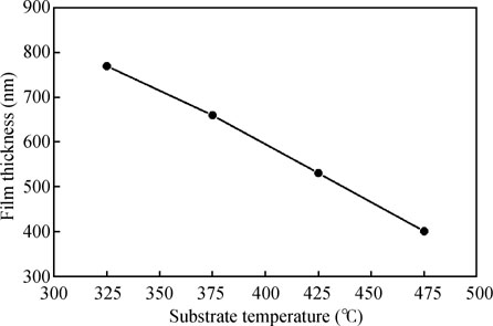
Fig. 1. Relationship between film thickness and substrate temperature for CdS films deposited by chemical spray pyrolysis.
Download figure:
Standard image3.2. Low angle X-ray diffraction (XRD) analysis
Low angle X-ray diffraction (low angle-XRD) is a widely used nondestructive technique for the structural characterization of different materials. Films deposited on glass were used for the low angle-XRD measurements. All low angle-XRD patterns were obtained at a grazing angle of 1°. Fig. 2 displays the low angle-XRD pattern of CdS thin films deposited at different substrate temperatures. Multiple diffraction peaks shows the polycrystalline nature of CdS thin films. As seen from the XRD pattern all films have diffraction peaks at 2θ = 24.79°, 26.52°, 28.11°, 36.63°, 43.56°, 47.75°, 51.79°, 58.29°, 66.95° and 70.85° corresponding to (100), (002), (101), (102), (110), (103), (201), (202), (203) and (211) diffraction planes respectively which are characteristic of hexagonal structure of CdS [JCPDS data file card # 41-1049]. It is interesting to note that the CdS films deposited at 325, 375, and  have preferred orientation of crystallites in (101) direction whereas the film deposited at
  have preferred orientation of crystallites in (002) direction. The sudden change in preferred orientation of crystallites from (101) to (002) may be attributed to the prevailing thermodynamical conditions at
  which favors the growth of crystallites along (002) plane.
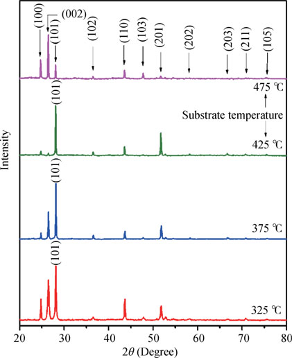
Fig. 2. (Color online) Low angle XRD pattern of CdS films prepared at different substrate temperatures.
Download figure:
Standard imageThe average crystallite ( ) size has been estimated using classical Scherrer's formula[27],
where λ is the wavelength of the X-ray used, β is full-width at half-maximum (FWHM) and θ is the Bragg diffraction angle. The estimated average crystallite size ( ) is shown in Fig. 3. The crystallite size was found to increase with an increase in substrate temperature which is in accordance with the previous reports[3, 31] for spraypyrolysed CdS thin films. Thus, increasing the substrate temperature decreases the density of the nucleation centers and under these circumstances, a smaller number of centers start to grow, resulting in large grains.

Fig. 3. Average crystallite size as a function of substrate temperature for CdS films deposited by chemical spray pyrolysis.
Download figure:
Standard image3.3. Raman spectroscopy analysis
Raman spectroscopy is a very powerful non-destructive technique used to investigate the structure of materials because it gives a fast and simple way to determine the phase of the material, whether it is amorphous, crystalline or nanocrystalline. Fig. 4 shows Raman spectra of CdS films deposited at different substrate temperatures by using chemical spray pyrolysis. As seen from the Raman spectra two major Raman peaks centered  and
and  were observed. They can be assigned to the first and second-order longitudinal optic (LO) phonon modes of CdS, respectively[32, 35]. Thus, formation of CdS films is further confirmed by Raman spectroscopy. With increase in substrate temperature significant change in the peak position was observed. The first order longitudinal optic (1LO) shifts from 300 to
  whereas second order longitudinal optic (2LO) shifts from 600 to
  when substrate temperature increased from 325 to
  , which can be due to decrease in the thickness of the film.
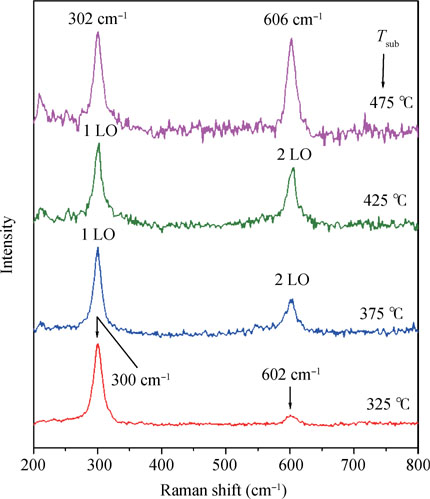
Fig. 4. Raman spectra of CdS films deposited at different substrate temperature by chemical spray pyrolysis.
Download figure:
Standard imageThe ratio of 2LO mode intensity to 1LO mode intensity (the overtone to fundamental ratio,  ), reflects the exciton-phonon coupling and is attributed to two main sources. The first is the increase of the overlap of the spatial wave functions of the electron and the hole in the electronic excited states in the nanoparticles, and the second is a big decrease of the lifetime of the excited state due to trapping on defects on the surface[36]. The ratio
  was calculated for the films deposited at different substrate temperatures. It was found that it increases from 0.12 to 0.96 when the substrate temperature increased from 325 to
  . These results indicate that the ratio
  depended on substrate temperature and hence average crystallite size of the CdS films (see Fig. 3). It increases with increase in average crystallite size. Our observations are in agreement with an earlier reported crystallite size dependent
  ratio for CdS films, both experimentally[35, 36] and theoretically[37, 38] and can be attributed to quantum confinement. Pan et al.[39] also found an increase in ratio from bulk CdS to CdS nanowires having larger dimensions.
3.4. X-ray photoelectron spectroscopy (XPS) analysis
The X-ray photoelectron spectroscopy (XPS) analysis was performed to determine the constituent elements present in the film. Fig. 5(a) shows XPS survey spectra (0–800 eV) of the CdS film deposited at substrate temperature  . The core level peaks corresponding to the elements Cd and S can be visibly seen in the spectra. In addition, it also shows the presence of C peak as well as O peak at
  285 and
  531 eV respectively as impurities. These contaminants have also been identified in CdS thin films deposited by CBD method by other workers[4, 41]. The core line of Cd 3d exhibited a doublet at
  404.88 and
  411.73 eV due to spin-orbit splitting resulting in Cd 3d5/2 and Cd 3d3/2 peaks with spin-orbit separation 6.85 eV [Fig. 5(b)]. These results are very well matched with the previously available data in Ref. [42]. Although the relative cross section of sulfur is small in comparison to the other elements, the sulfur peaks are sensitive to the chemical environment. The lower binding energy peak at 161.5 eV is indicative of metal sulfide. The S 2p level was resolved into a single spin-orbit splitting of Gaussian component [Fig. 5(c)]. The spin-orbit splitting separation was allowed to vary during fitting. The binding energy value of S 2p3/2 is
  161.5 eV and S 2p1/2 is
  162.7 eV with separation of 1.2 eV. This characteristic binding energy of S 2p3/2 and S 2p1/2 of CdS agree with those reported in Ref. [42]. The quantitative studies were carried out using normalized peak intensities of Cd 3d and S 2p spectra taking into consideration the relative sensitivity factor (RSF) of the spectrometer, provided by the instrument manufacturer (for Cd 3d is 6.62 and for S 2p is 0.67). The atomic percentage of Cd is 46%, S is 45% and 8% for O for the CdS film deposited at substrate temperature
  . The Cd/S ratio is 1.02, greater than unity in the present study which may be due to the partial oxidation of CdS film[40].
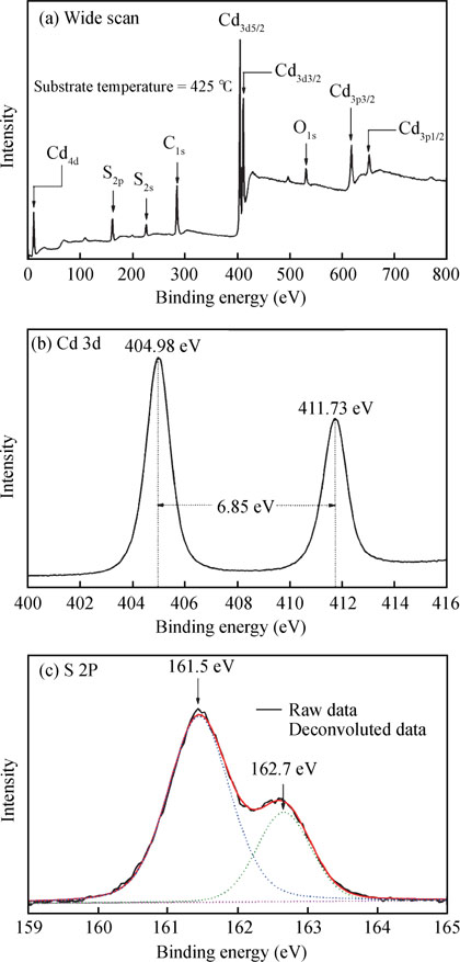
Fig. 5. Typical XPS spectra for CdS film deposited at substrate temperature  by CSP method. (a) Wide scan in the range 0–800 eV. (b) Cd 3d spectra in the range 400–416 eV. (c) S 2p spectra in the range 158–166 eV.
Download figure:
Standard image3.5. Field emission scanning electron microscopy analysis
Fig. 6 shows the FESEM images of CdS films deposited at different substrate temperatures. As seen all films are dense, homogeneous, and free from flaws and cracks. From FESEM images it is clear that the morphological properties of CdS films strongly depend on substrate temperature. As seen from the FESEM images, the film deposited at  exhibits sheetlike morphology with average length
  and width 80–140 nm [Fig. 6(a)]. These sheets tangle into each other forming film and are made up of nanoparticles in the range of 10 to 50 nm. The film deposited at
  shows faceted prismatic shape of nanoparticles having average length 100–250 nm and width 40–100 nm [Fig. 6(b)]. The film deposited at
  shows the same prismatic shape-like morphology, however, with increased particle size (
 200–550 nm) [Fig. 6(c)]. Finally, in the case of the film deposited at
  , instead of prismatic shape, the irregular rodlike structure having average 200–400 nm and width 60–100 nm were observed [Fig. 6(d)]. It may be noted that the CdS films prepared at this temperature have (002) preferred orientation which favors rodlike morphology instead of prismatic structure[43, 44].
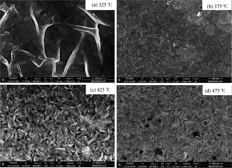
Fig. 6. FESEM images of CdS films prepared at substrate temperatures (a)  , (b)
, (b)  , (c)
, (c)  and (d)
  .
.
Download figure:
Standard image3.6. Atomic force microscopy analysis
Fig. 7 shows surface morphology of CdS films investigated by non-contact atomic force microscopy (NC-AFM). All images were measured for an area of  deposited on glass substrates. All films show complete coverage over the glass substrates. With change in substrate temperature, the significant differences in the surface morphology and topography can be seen. As seen from Fig. 7(a), the CdS film deposited at
  is composed of dense topography having irregular grains. The root-mean square (RMS) surface roughness of the films is calculated using the equipment's software routine and was found to be 62.83 nm. The CdS film deposited at
  [Fig. 7(b)] shows faceted shape like topography with widely separated tiny clusters of CdS having well-defined grain boundaries. For this film the RMS surface roughness was found to be 66.30 nm. With increase in substrate temperature to
  [Fig. 7(c)], one can observe the agglomeration of tiny clusters to form non-uniform larger clusters of CdS with increased surface roughness of 68.28 nm. Finally, the CdS film deposited at
  [Fig. 7(d)] shows topography with highly dense clusters of CdS having well-defined grain boundaries. For this film the RMS surface roughness was found to be 68.30 nm. Therefore, it is concluded that with increase in substrate temperature, the topography of CdS films changes from irregular grains to highly dense clusters having well-defined grain boundaries with enhanced surface roughness.
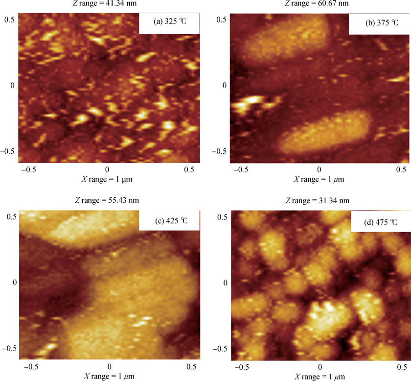
Fig. 7. AFM images of CdS films prepared at (a)  , (b)
, (b)  , (c)
, (c)  and (d)
  by CSP method.
Download figure:
Standard image3.7. Transmission electron microscopy analysis
The TEM image of CdS films deposited at 325,  and corresponding selected area electron diffraction (SAED) pattern are shown in Fig. 8. As seen from the figure, the film deposited at
  [Fig. 8(a)] clearly shows the formation of tangled sheets with bunches of nanoparticles. The length and width of these bunches vary in the range of 60–125 nm and 40–60 nm, respectively. These results are consistent with FE-SEM analysis (see Fig. 6). The film deposited at
  [Fig. 8(b)] shows highly dense quantum dot sized nano-particles having size around 5–10 nm. Fig. 8(c) shows SAED pattern of CdS film deposited at substrate temperature
  . The existence of ring-like nature in SAED pattern indicates that the film is polycrystalline which resembles low angle XRD pattern (see Fig. 2).
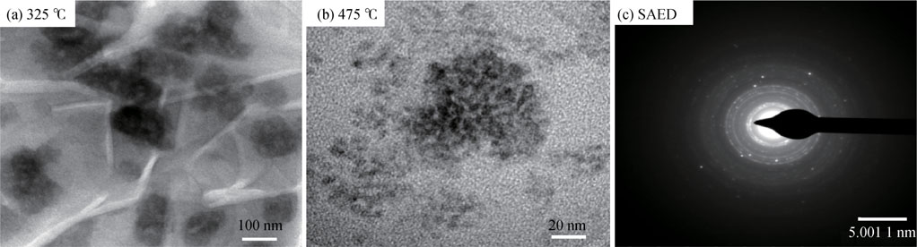
Fig. 8. TEM images of CdS films deposited at substrate temperature of (a)  , (b)
, (b)  and (c) SAED pattern of CdS film deposited at substrate temperature of
  .
.
Download figure:
Standard image3.8. UV–visible spectroscopy analysis
Fig. 9 displays the transmittance curves in the range 300–800 nm of CdS thin films prepared at different substrate temperatures. The transmission strongly depends on the film structure, which is determined by the preparation methods, film thickness and deposition conditions[3]. It has been observed that an increase in substrate temperature improves the transmission of CdS films. In chemical spray pyrolysis method the change in transmission of CdS thin films with substrate temperature is controversial. Ashour[31] related the improvement of the transmittance of CdS films with substrate temperature to a decrease in thickness or the improvement in perfection and stoichiometry of the films. On the other hand, Acosta et al.[45] interpreted the decrease in transmittance with the substrate temperature to the structural and morphological changes. We think that improvement in transmission of CdS thin films with temperature can be both due to decrease in thickness (see Fig. 1) and improvement in crystalline nature of the film (see Fig. 2). A sharp absorption edge is observed in the visible region, indicating good crystallinity and low defect density near the band edge. The absence of interference fringes in the films' transmittance spectra indicates that they have rough surface morphology. Atomic force microscopy analysis further supports this (see Fig. 7).
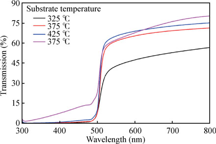
Fig. 9. (Color online) Transmittance spectra of CdS films deposited at various substrate temperatures using CSP method.
Download figure:
Standard imageIn the direct transition semiconductor, the optical energy band gap  and the optical absorption coefficient
  are related by[46]

where α is the absorption coefficient, B is the optical density of state and E is the photon energy. The α can be calculated from the transmittance of the films using

where d is the thickness of the films and T is the transmittance. Therefore, the optical band gap is obtained by extrapolating the tangential line to the photon energy  axis in the plot of
  as a function of photon energy,
  (Tauc plot). The Tauc plots for CdS films deposited at different substrate temperatures using CSP method is shown in Fig. 10. The inset shows variation of optical gap as a function of substrate temperature for CdS thin films deposited using CSP method As seen the band gap increases from 2.43 to 2.99 eV when substrate temperature increased from 325 to
  . An increase in band gap of CdS films with increase in substrate temperature is well established in Refs. [3, 31]. The band gap of bulk CdS is 2.42 eV. The values of the band gap were higher than the band gap of bulk CdS (2.42 eV)[47]. Raghvendra et al.[48] and Dongre et al.[49] have also reported high band gap values for CdS films deposited by chemical bath deposition method and sonochemical process respectively. These results suggest that the high band gap makes CdS a more effective window material in photovoltaic applications like the CdS/CdTe and CdS/Cu2S solar cells.

Fig. 10. (Color online) Tauc plots for CdS films deposited at different substrate temperatures. The inset shows variation of optical gap as a function of substrate temperature for CdS thin films deposited using CSP method.
Download figure:
Standard image3.9. Photoluminescence spectroscopy analysis
Fig. 11 shows room temperature photoluminescence (PL) spectra with 430 nm Argon ion laser as the excitation source for CdS films deposited at different substrate temperatures using CSP method. As seen from the figure, there are three prominent emission peaks observed at  546, 579 and 612 nm for all the CdS films. The high intensity peak
  546 nm is known as the near band edge emission (NBE) which is nearly the same as the optical band gap estimated using transmission spectra. This emission occurs due to recombination of free conduction electron with the holes in the acceptor levels and various reasons reported by Pedrotti et al.[5] and Kulp et al.[51]. It is well known that surface defects and shallow and deep trap states play an important role in the luminescent properties of nanocrystalline CdS thin films[52]. Therefore, the other two peaks
  579 and 612 nm shown in the PL spectra may originate from different surface level defects present in the CdS thin films. Surface defects in nanocrystalline CdS are created due to the creation of trap levels[53]. Some other defects are also created due to the S and Cd ion vacancies or may be due to being adsorbed in the interstitial surface[54]. According to Panda and others[5], the
  traps may form on the surface of nanocrystalline CdS due to migration of photo-generated holes. Recombination of the photo-generated electrons from the conduction band traps with holes at
  traps competes against a rather efficient h+ transfer, leading to very weak emission. The observed weak emission at 579 and 612 nm in the PL spectra further support this conjecture. It is interesting to note that intensities of all emission peaks decrease with increase in substrate temperature. Being small crystallite size, the surface to volume ratio of nanocrystalline CdS is quite high. As a result the surface related defects are dominant in nanocrystalline CdS films. With increase in substrate temperature the average crystallite size of CdS increases (see Fig. 3) and consequently, the surface to volume ratio declines. As a result, the intensities of the defect related peaks show gradual decreasing trend with increase in substrate temperature. The observed weak emission in the range of 650–750 nm observed from the synthesized CdS films is due to trapped state emission[55].

Fig. 11. (Color online) Photoluminescence spectra of CdS films deposited at different substrate temperatures using CSP method.
Download figure:
Standard image3.10. Electrical properties
The resistivity values of the different films were measured by using van der Pauw geometry. For the resistivity measurement, the four ohmic contacts were made by using indium wire at the four corners of the film sample. Sheet resistance  of a given CdS film was calculated by using the following equation

where R is the average resistance measured between four points of the film. Table 2 shows variation of sheet resistance as a function of substrate temperature of CdS thin films deposited using CSP method.
Table 2. Variation in sheet resistance as a function of substrate temperature of CdS thin films.
Substrate temperature  |
Sheet resistance (M  ) ) |
|---|---|
| 325 | 51.03 |
| 375 | 33.07 |
| 425 | 29.03 |
| 475 | 21.88 |
As seen from the table all films exhibited semiconductor behavior with the sheet resistance gradually decreasing from 51.03 to 21.88 M  over the entire range of substrate temperature studied. The gradual decrease in the sheet resistance can be attributed to the increase in crystallinity of the films with increase in substrate temperature.
4. Conclusions
In the present work, cadmium sulfide (CdS) thin films have been prepared by simple, cost effective and home-built chemical spray pyrolysis (CSP) method by spraying the precursor solution directly onto the soda lime glass (SLG) substrates. The influences of substrate temperature on structural, optical, morphological and electrical properties of CdS films have been investigated systematically. The synthesized films were characterized by using various techniques such as low angle XRD, FE-SEM, TEM, XPS, AFM as well as Raman, PL spectroscopy and UV–visible spectroscopy etc. The formation of CdS films has been confirmed by low angle X-ray diffraction, Raman spectroscopy and X-ray photoelectron spectroscopy analysis. It has been observed that the thickness of CdS decreases with increase in substrate temperature. Multiple diffraction peaks observed in XRD pattern shows that the CdS films are polycrystalline and has hexagonal structure. In addition, the preferred orientation of crystallites shifts from (101) to (002) direction with increase in substrate temperature. From Raman spectroscopy analysis it has been found that the exciton-phonon coupling ( /I1LO) increases from 0.12 to 0.96 when substrate temperature increased from 325 to
  . These results indicate that exciton-phonon coupling in CdS depends on substrate temperature and hence average crystallite size of the CdS films. The surface morphology and topography of CdS films investigated by FE-SEM and AFM are critically dependent on substrate temperature. The UV–visible spectroscopy analysis showed that the optical band gap increases from 2.43 to 2.99 eV when substrate temperature increased from 325 to
  . Such high band gap CdS may be useful as window material in heterojunctions like CdS/CdTe and CdS/Cu2S solar cells. However, further studies are needed to improve the quality of CdS films so as to realize them in photoconductor and solar cell applications.
Acknowledgement
One of the authors SRJ is grateful to University Grants Commission, New Delhi for special financial support under UPE program.
Footnotes
- *
Project supported by the Department of Science and Technology (DST), Ministry of New and Renewable Energy (MNRE), Government of India, New Delhi.