
Abstract
Zinc oxide (ZnO) shows great potential in electronics, but its large intrinsic thermal conductivity limits its thermoelectric applications. In this work, we explore the significant carrier transport capacity and diameter-dependent thermoelectric characteristics of wurtzite-ZnO 〈0001〉 nanowires based on first-principles and molecular dynamics simulations. Under the synergistic effect of band degeneracy and weak phonon–electron scattering, P-type (ZnO)73 nanowires achieve an ultra-high power factor above 1500 μW⋅cm−1⋅K−2 over a wide temperature range. The lattice thermal conductivity and carrier transport properties of ZnO nanowires exhibit a strong diameter size dependence. When the ZnO nanowire diameter exceeds 12.72 Å, the carrier transport properties increase significantly, while the thermal conductivity shows a slight increase with the diameter size, resulting in a ZT value of up to 6.4 at 700 K for P-type (ZnO)73. For the first time, the size effect is also illustrated by introducing two geometrical configurations of the ZnO nanowires. This work theoretically depicts the size optimization strategy for the thermoelectric conversion of ZnO nanowires.
Export citation and abstract BibTeX RIS
1. Introduction
Thermoelectric materials are characterized by the ability to directly convert thermal energy into electrical energy.[1,2] The thermoelectric properties of materials are usually evaluated using the dimensionless figure of merit ZT = S2 σT/κ, where S, σ, T and κ represent the Seebeck coefficient, electrical conductivity, temperature and thermal conductivity (the sum of lattice thermal conductivity κl and electronic thermal conductivity κe), respectively. These three parameters normally exhibit interdependence. Hence, enhancing thermoelectric performance by only optimizing one parameter has been proven to be a challenging endeavor.[1]
Zinc oxide (ZnO) is a wide band gap semiconductor material that is widely used in piezoelectrics and has great potential in the fields of optics, electronics, photoelectronics, acoustoelectronics and so on.[3–5] It has good carrier transport capabilities, but its extremely high intrinsic thermal conductivity (> 40 W⋅m−1⋅K−1) limits its thermoelectric applications. Experimental studies and theoretical computations have demonstrated that dimensionality reduction is a potential means of improving its thermoelectric performance.[6–8] Wurtzite-ZnO 〈0001〉 nanowires have been shown to be a reliable low-dimensional ZnO nanowire conformation. They have been selected as the subject of this work to investigate their thermoelectric properties based on first-principles calculations.[9] In practical applications, ZnO nanowires are often used as a dopant or in arrays.[10,11] When the diameter of the nanowires is reduced, the number of contained nanowires increases accordingly for the same doping concentration (volume fraction) or surface area due to array growth. As the diameter of a nanowire approaches the nanoscale, the size effects of phonons and electrons become more pronounced, making the study of size effects even more significant.
Efforts have been made to improve the thermoelectric properties of ZnO nanowires through doping with elements such as Al, Ga and Sb. These doping strategies have been found to improve the electrical transport characteristics of the nanowires while simultaneously reducing thermal conductivity.[12] It was also suggested that the W (wurtzite)–H (graphitic polymorph) phase transition under strain could potentially improve the thermoelectric properties of ZnO nanowires, providing a novel insight for optimization.[13] Although several studies have endeavored to enhance the thermoelectric performance of ZnO nanowires, the related size-effect questions are rarely addressed. A comprehensive analysis of the thermoelectric properties of ZnO nanowires is lacking, including the roles of nanowire configuration, diameter and temperature, which are important when studying low-dimensional materials.[7] When materials exist in a low-dimensional form, phonon and electron transport processes are both confined in the low-dimensional direction, so the study of size effects is essential.[7,14,15] In addition, previous studies have predominantly focused on N-type ZnO nanowires, neglecting the P-type semiconductor properties of ZnO nanowires, which constrains further development of thermoelectric properties.
In this study, we investigate the thermoelectric properties of ZnO nanowires with four different diameters in the temperature range of 300 K to 700 K using first-principles calculations. The rest of the article is organized as follows. The computational methods are introduced in Section 2. The geometric models are presented in Subsection 3.1 and the electronic properties, including band structure, charge density distribution and electron relaxation time, are investigated in Subsection 3.2. Lattice thermal conductivity is studied in Subsection 3.3. The underlying mechanism of the thermoelectric performance is discussed with the analysis of the band structure, charge density distribution, phonon–electron scattering intensity and structural configuration of ZnO nanowires in Subsection 3.4. The main conclusions are summarized in Section 4.
2. Computational methods
The optimization of geometric structure and the calculation of electronic properties are all based on the density functional theory (DFT), using the Vienna ab initio simulation package.[16] The projected augmented wave method with the Perdew–Burke–Ernzerhof generalized gradient approximation (GGA) is chosen for the electronic exchange–correlation function.[17,18] In the case of strongly correlated systems featuring d and f orbital electrons, there is a pronounced on-site Coulomb interaction among electrons. However, the local density approximation or GGA in exchange–correlation functionals inadequately describes the strong on-site Coulomb interaction among electrons.[19] Due to the fact that ZnO is a metal oxide composed of transition metal elements with localized d orbital electrons and oxygen elements with localized p orbital electrons, the traditional GGA method is insufficient for providing an accurate depiction. This aspect has often been overlooked in previous research,[12,13] which could lead to an underestimation of the band gap and inaccurate descriptions of electronic properties. Here, the Hubbard parameter U is introduced to describe the strong correlation interactions between atoms, termed as the GGA + U method. The GGA + U method is capable of precisely describing the electronic structure of doped transition metals, transition metal elements and oxides with localized oxygen elements.[19–21] In energy calculations, electrons are treated with spin polarization. Recognizing that the conventional GGA method typically underestimates the band gap of metal oxides, the GGA + U approach is employed to correct this band gap assessment. In the calculations, the Hubbard parameter U for the 3d state of Zn and the 2p state of O are set to 5.5 eV and 8.0 eV, respectively.[21] The cutoff energy is set to 500 eV, and a Monkhorst–Pack k-mesh is set as (1 1 5) for structural optimization and (1 1 9) for static self-consistent calculation. Since the present study focuses on the electrical properties of the nanowire in the axial direction (c direction), vacuum layers of 10 Å–15 Å are added in the a and b directions to avoid the interaction between nanowires due to the periodic boundary condition.
The physical quantities related to the electron transport properties, including Seebeck coefficient S, electrical conductivity σ and electronic thermal conductivity κe, are all derived from solving the Boltzmann transport equation using the BoltzTrap2 software package.[22] The electron relaxation time τ also needs to be calculated, since the BoltzTrap2 results are in the form of σ/τ and κe/τ. The deformation potential theory proposed by Bardeen and Shockley is chosen to solve the electron relaxation time τ,[23]
where μ1D is the 1D material's carrier mobility and m* = ℏ2[∂2 ε( k )/∂k 2]−1 is the inertia effective mass of the carrier related to the valence band maximum (VBM) and conduction band minimum (CBM) band energy, where ℏ is the Planck constant and k is the electron wave-vector. C1D represents the elastic modulus in the axial direction, determined by C1D = (1/l0)(∂2 E/∂(Δl/l0)2), where l0 is the lattice constant in the axial direction and E is the total energy of the system. The deformation potential constant El has a similar expression to the elastic modulus, El = ∂Eedge/∂(Δl/l0), where Eedge means the energy of the VBM or CBM, which depends on whether the carrier type is hole (P-type semiconductor) or electron (N-type semiconductor). In this work, the strain rate is set in the range of ±1.5% and the calculation of electronic properties is performed every 0.5% strain. It can be observed that the deformation potential constant is related to the band structure and lattice deformation, indicating its consideration of electron–phonon coupling effects. However, it is crucial to acknowledge that this parameter only reflects the influence of electrons in band edge states. This approximation is deemed acceptable and the deformation potential constant finds extensive applications in the computation of electron relaxation times for one-dimensional materials.[24–27] The electron relaxation time obtained through deformation potential theory comprehensively considers the effects of phonon–electron coupling and temperature and will directly impact the electrical conductivity and electronic thermal conductivity, thereby ultimately determining the ZT value.
In this work, the equilibrium molecular dynamics (EMD) method is employed to calculate the lattice thermal conductivities of ZnO nanowires. Heat conduction is a non-equilibrium process, while the EMD method calculates the thermal conductivity by simulating the equilibrium state of the system. The core theory is the linear response theory: within the linear response range, the Green–Kubo formula can be used to connect the transport coefficient of the non-equilibrium process with the fluctuation of the corresponding physical quantity in the equilibrium state.[28,29] The Green–Kubo formula points out that the transport coefficient is equal to the integral of the autocorrelation function over the correlation time. In the heat conduction process, the thermal conductivity is the integral of the autocorrelation function of heat flow. Through the Green–Kubo formula, the lattice thermal conductivity can be calculated by an equilibrium simulation. The Green–Kubo formula for calculating the lattice thermal conductivity is as follows:[30]
where κμν
(t) (μ, v = x, y, z) is the thermal conductivity tensor, t' is the correlation time, kB is the Boltzmann constant, T is the temperature and Cμν
(t) = 〈Jμ
(0)Jν
(t)〉 is the heat current autocorrelation function, where  represents the heat flux and angle brackets represent the statistical average over the time origin. The heat flux is obtained by summing the product of the space position vector
ri
(t) and the energy ei
(t) of each particle at a certain moment t, where the energy ei
includes the kinetic energy
represents the heat flux and angle brackets represent the statistical average over the time origin. The heat flux is obtained by summing the product of the space position vector
ri
(t) and the energy ei
(t) of each particle at a certain moment t, where the energy ei
includes the kinetic energy  and the potential energy of the interaction between particles (1/2)∑ϕ(rij
).
and the potential energy of the interaction between particles (1/2)∑ϕ(rij
).
The open source molecular dynamics software LAMMPS is employed for the molecular dynamics simulation. The interatomic interaction potential is described by the Buckingham potential, which is characterized by comprehensively considering the long-range and short-range Coulomb interactions between charges. Therefore, it is widely used in the relevant molecular dynamics calculation of ionic oxides represented by ZnO.[31,32] The expression is as follows:
where rij is the distance between ion i and ion j, qi and qj are the charges of ion i and ion j, respectively, A, ρ and C are related parameters, which are shown in Table 1. In the Buckingham potential expression, the first term is the long-range Coulomb force, and the second and third terms are the short-range repulsion and attraction, respectively. Ewald method is used in the treatment of long-range force, which ensures the computation efficiency and convergence.
Table 1. Buckingham potential related parameters
| Ion pair | A (eV) | ρ (Å) | C (eV⋅Å−6) |
|---|---|---|---|
| O2−–O2− | 9547.96 | 0.21916 | 32.0 |
| Zn2+–O2− | 529.70 | 0.3581 | 0 |
| Zn2+–Zn2+ | 0 | 0 | 0 |
In the EMD simulation, the step size of 0.001 ps is maintained. Firstly, the energy relaxation of the system is simulated at 500 ps in the NVT ensemble (canonical ensemble) to reach the thermodynamic equilibrium state. Then the NVT ensemble is removed and the NVE ensemble (micro-canonical ensemble) is added for equilibrium simulations, by setting the amount of correlation data to 1000, the number of sampling interval steps to 10, the number of heat flow autocorrelation functions to 10 and the total number of output simulation steps to 1000000.
3. Results and discussion
3.1. Geometric model
The wurtzite-ZnO 〈0001〉 nanowire model has been verified by both experiments and simulations to be the most reasonable ZnO nanowire configuration.[9] That is, the [0001] surface orientation of bulk wurtzite-ZnO is used as the cross-sectional foundation of the ZnO nanowire. As shown in Fig. 1, four wurtzite-ZnO 〈0001〉 nanowires with different diameters are selected for the present computational study and the configurations exhibit direct band gap features, where n indicates the number of Zn atoms/O atoms in a primitive cell. In the subsequent text, the different nanowire models will be marked as (ZnO)n .
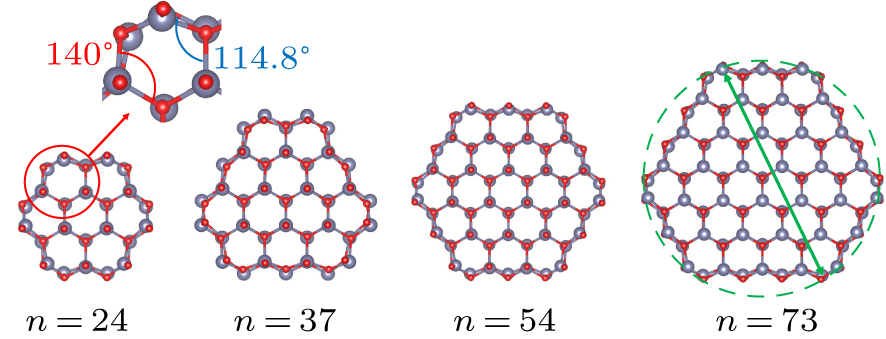
Fig. 1. Cross section view of wurtzite-ZnO 〈0001〉 nanowire models. From left to right: (ZnO)24, (ZnO)37, (ZnO)54, and (ZnO)73.
Download figure:
Standard imageThe geometric models are established by slicing the ZnO bulk along the [0001] direction using Materials Studio. The lattice constants in a and b directions differ because of variations in cross-sectional shapes (detailed in Table 2). A certain length of vacuum layer needs to be set around the model to ensure that the calculated nanowires are not affected by the periodic boundary in a and b directions. The initial lattice constant in c direction is 5.19 Å, which increases significantly after structural relaxation optimization (shown in Table 2).
Table 2. Diameters and lattice constants of wurtzite-ZnO〈0001〉 nanowire models
| Model | Diameter (Å) | Cell parameters (Å) | |
|---|---|---|---|
| La or Lb | Lc | ||
| (ZnO)24 | 10.06 | 20 | 5.393 |
| (ZnO)37 | 12.72 | 25 | 5.376 |
| (ZnO)54 | 16.56 | 30 | 5.361 |
| (ZnO)73 | 19.84 | 40 | 5.358 |
Given that the intrinsic lattice structure of ZnO in the a–b plane forms a regular hexagon, the bond angle of Zn–O–Zn and O–Zn–O should measure 120°. Following structural optimization, the axial view reveals notable displacements in the outermost Zn and O atoms (shown in Fig. 1). The bond angle of Zn–O–Zn on the a–b plane decreases to 114.8°, while the bond angle of O–Zn–O increases to 140°. The diameter of the nanowire is determined by selecting the distance between the two atoms that are furthest apart within the a–b plane of the nanowire (also the diameter of the smallest outer tangent circle of the nanowire, as shown in Fig. 1). Based on the geometric model established above, the thermal transport and electrical transport properties of ZnO nanowires are studied comprehensively.
3.2. Electronic properties
In this subsection, various charge carrier related properties of ZnO nanowires are discussed, starting with the electronic band structure and properties. Then, the relevant parameters in the calculation of carrier mobility and electron relaxation time are analyzed, and finally the carrier transport properties of ZnO nanowires are presented.
3.2.1. Band structure
The Γ–Z is selected as the high symmetry path for band calculation, since the carriers only transport in the axial direction. (ZnO)n nanowires (n = 24, 37, 54 and 73) show an obvious direct band gap, as shown in Fig. 2. All the VBMs and CBMs are located at the Γ point. Note that traditional GGA methods in previous studies significantly underestimate the band structure of ZnO nanowires in contrast to the GGA + U method employed in present study.[33,34]

Fig. 2. Band structure of (a) (ZnO)24, (b) (ZnO)37, (c) (ZnO)54 and (d) (ZnO)73.
Download figure:
Standard imageAs shown in Table 3, the direct band gap decreases monotonously from 2.02 eV to 1.67 eV with the increase of nanowire diameter. This is consistent with the trend of band gap variation with diameter observed in previous studies.[33,34] The band gap of ZnO nanowires exhibits a notable reduction compared with the bulk phase of ZnO (3.3 eV), which is favorable for enhancing carrier transport. From the Γ point, the energy bands of both VBM and CBM are half-parabolic, while the curvature of the CBM is more pronounced compared with that of the VBM. The morphological difference between the valence band and the conduction band results in a difference of carrier transport capacity. Details of the charge carrier transport properties are discussed in the following sections.
Table 3. Band gap, VBM and CBM of (ZnO)24, (ZnO)37, (ZnO)54 and (ZnO)73
| n | 24 | 37 | 54 | 73 |
|---|---|---|---|---|
| Band gap (eV) | 2.02 | 1.87 | 1.75 | 1.67 |
| VBM (eV) | −0.049 | −0.056 | −0.056 | −0.047 |
| CBM (eV) | 1.97 | 1.82 | 1.69 | 1.62 |
3.2.2. Charge density distribution
ZnO is a typical metal oxide. Zn and O atoms are bonded through ionic interactions, resulting from the transfer of charge. The Zn atom exhibits a positive valence state, while the O atom displays a negative valence state. Oppositely charged Zn2+ and O2− ions interact, culminating in the formation of an ionic bond. The total charge density distribution calculated by the DFT is shown in Fig. 3(a). The uniform distribution of charge around the Zn and O atoms suggests the existence of a stable ionic bond between these two elements within the ZnO nanowires.
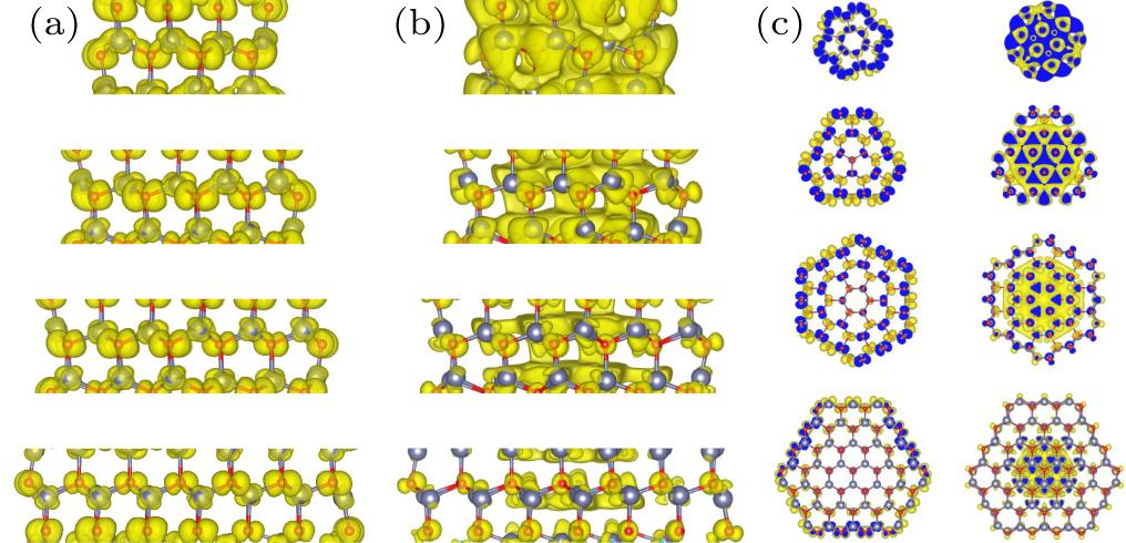
Fig. 3. (a) Charge density of the total state, (b) radial section and (c) axial view of VBM and CBM states for (ZnO)24, (ZnO)37, (ZnO)54 and (ZnO)73.
Download figure:
Standard imageFigures 3(b) and 3(c) supplement this understanding by illustrating the charge distribution of the VBM and CBM in axial section and radial view. The charges of the VBM states are distributed along the outside of the nanowire, while the CBM states are mainly distributed inside the nanowire. Moreover, in the VBM and CBM states, the charge distribution around the O and Zn atoms shows characteristics aligned with the p and d orbitals, which is consistent with the valence electron distribution of Zn and O atoms in ZnO. Another obvious feature is that the p and d orbital charges in the CBM state evidently overlap with the Zn2+–O2− ion bonds in the axial direction. In contrast, within the VBM state, only parts of the p and d orbitals of (ZnO)24 and (ZnO)37 overlap, and the overall charge distribution is discrete.
For a more comprehensive comparison of the electronic structures among the four nanowire models, the total density of states (DOS) and the projected DOS of atomic orbitals are calculated as shown in Fig. S1. It can be observed that in the region below the Fermi level, due to the obvious splitting phenomenon of the valence band, the DOS is evenly distributed. In the region above the Fermi level, there are few conduction bands, resulting in a prominent peak in the DOS. Near the CBM, the DOS exhibits a clear one-dimensional characteristic of E−1/2 function, whereas near the VBM, there is no obvious E−1/2 function characteristic due to the overlay of DOS in multiple energy bands. The original valence electron arrangements of the O and Zn atoms are 2s22p4 and 3d104s2, respectively. When combined by the ionic bond, the two electrons originally located in 4s2 of the Zn atom are transferred to the 2p4 orbital of the O atom, which is consistent with the DOS calculation result. The 2p orbital of the O atom and the 3d orbital of the Zn atom contribute most to the DOS, which is in harmony with the charge density distribution result. In the region near the Fermi level, the orbital density of states of the O 2p orbital is the main participant, while the Zn 3d orbital plays a secondary role. It can also be observed from the charge density distribution that the electron cloud around the O atom is significantly more concentrated than that of the Zn atom.
3.2.3. Electron relaxation time
To obtain the electron transport properties of ZnO nanowires, the electron relaxation time and carrier mobility must be calculated, which was missed in previous research on ZnO nanowires. In this work, the electron transport properties of ZnO nanowires in the temperature range of 300 K–700 K are discussed to obtain a more comprehensive conclusion.
As mentioned in Section 2, the deformation potential theory is employed to compute the electron relaxation time. In the deformation potential theory, elastic modulus C1D, inertial effective mass m* and deformation potential constant El are three uncoupled parameters. Thermoelectric performance can be effectively characterized through the analysis of these three parameters. The corresponding calculation results are shown in Table 4, and the data for fitting the deformation potential constant and elastic modulus are provided in Figs. S2–S5.
Table 4. Deformation potential constant, inertial effective mass and elastic modulus for (ZnO)24, (ZnO)37, (ZnO)54 and (ZnO)73.
| P-type | (ZnO)24 | (ZnO)37 | (ZnO)54 | (ZnO)73 |
|---|---|---|---|---|
| m*/m0 | 1.4 | 1.6 | 2 | 1.34 |
| C1D (10−11 J⋅m−1) | 1.38 | 2.20 | 3.22 | 4.49 |
| El (eV) | 1.14 | 1.31 | 0.34 | 0.22 |
| N-type | (ZnO)24 | (ZnO)37 | (ZnO)54 | (ZnO)73 |
|---|---|---|---|---|
| m*/m0 | 0.30 | 0.27 | 0.26 | 0.18 |
| C1D (10−11 J⋅m−1) | 1.38 | 2.20 | 3.22 | 4.49 |
| El (eV) | 2.09 | 4.07 | 3.27 | 2.86 |
Elastic modulus is a physical quantity that describes the elasticity of a material. It refers to the proportional coefficient between strain and stress during elastic deformation. Among the three parameters in the deformation potential theory, elastic modulus is the only parameter that is not affected by the carrier type. In this work, the modulus of elasticity increases linearly with increasing nanowire diameter.
The understanding of the inertial effective mass can be compared with the mass in Newton's second law; that is, the smaller the mass, the easier it is for the object (carrier) to move. For P-type semiconductors, the carriers are holes at the top of the valence bands, while the carriers of N-type semiconductors are electrons at the bottom of the conduction bands. Note that the hole effective mass is significantly larger than the electron effective mass, corresponding to the CBM slope being significantly larger than the VBM slope at the Γ point in Fig. 2. As the diameter increases, the CBM continues to drop, leading to a decrease in effective mass.
Deformation potential constant is a physical quantity to describe the response of band structure to material lattice deformation. The deformation potential constant represents the energy change of holes at VBM or electrons at CBM along the transmission direction when the material is deformed. The calculations reveal two prominent results. Firstly, the deformation potential constants for P-type materials are notably smaller than those for N-type materials. Secondly, there is a clear trend where the deformation potential constant increases from (ZnO)24 to (ZnO)37, followed by a subsequent decline at (ZnO)54 and (ZnO)73.
3.2.4. Carrier transport properties
After obtaining the electron relaxation time based on the deformation potential theory, the Seebeck coefficient S, electrical conductivity σ and electronic thermal conductivity κe and power factor PF are calculated from the solution of Boltzmann equation and electron relaxation time theory. The carrier concentrations discussed in this section correspond to the maximum ZT value and are typically on the order of 1019 cm−3 to 1020 cm−3.
It is most striking in Fig. 4 that the transport parameters related to P-type are 2–3 times higher than those of N-type, and P-type (ZnO)73 exhibits an ultra-high power factor over 1500 μW⋅cm−1⋅K−2 at 300 K. Among the transport coefficients, the Seebeck coefficient shows the least difference between the P-type and N-type, with the Seebeck coefficient of the P-type being 14%–82% higher than that of the N-type. In terms of electrical conductivity, the gap between P–N type is more pronounced. The electrical conductivity of P-type is averagely 2.36–7.58 times that of N-type. Correspondingly, the electronic thermal conductivity of P-type is 3.2–10 times that of N-type.
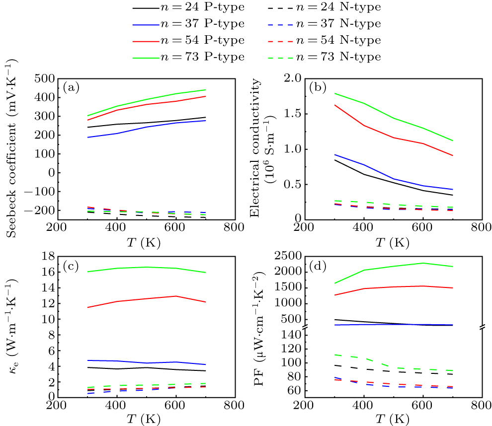
Fig. 4. (a) Seebeck coefficient, (b) electrical conductivity, (c) electronic thermal conductivity and (d) power factor of (ZnO)24, (ZnO)37, (ZnO)54, and (ZnO)73.
Download figure:
Standard imageA comparison of the carrier transport performance of the P–N type accurately corresponds to the energy band properties of ZnO nanowires. As shown in Fig. 2, the valence band of ZnO nanowires exhibits a dense band structure, with energy levels near the VBM closely spaced. In contrast, the conduction band region features a relatively thin band structure, with energy levels near the CBM also being highly independent. Pei et al. proved that when the energy difference between energy bands is less than 2kB T (the value ranges from 0.052 eV to 0.12 eV in the temperature range from 300 K to 700 K), the degeneracy effect between energy bands will enhance the thermoelectric properties.[35] In this energy range, ZnO nanowires exhibit 2–4 energy bands near the VBM available for participating in carrier transport, whereas only the CBM contributes to carrier transport in the conduction bands. The proportion of bands participating in carrier transport within the valence and conduction bands exhibits a noticeable correlation with P–N carrier transport parameters, such as electrical conductivity.
Apart from the band degeneracy effect in the valence band of ZnO nanowires, the weaker phonon–electron scattering intensity near the VBM further enhances the P-type transport properties. The deformation potential constant is a physical parameter that characterizes how the energy band structure responds to the lattice deformation. It also serves as an indicator of the strength of interaction between carriers in the VBM or CBM and acoustic phonons. Given that the deformation potential constant is squared in the denominator of the relaxation time equation (Eq. (1)), its influence on the final relaxation time result is prominent. The Seebeck coefficient and electrical conductivity of (ZnO)37 do not show a significant improvement compared with (ZnO)24, whereas (ZnO)54 and (ZnO)73 exhibit a significant enhancement in carrier transport properties. This is notably correlated with the pattern of deformation potential constant changes with diameter. Interestingly, the deformation potential constant of N-type is significantly greater than that of P-type, aligning perfectly with the higher carrier transport characteristics of P-type compared with N-type. These phenomena collectively indicate that the phonon–electron scattering exerts a direct influence on the carrier transport in ZnO nanowires. The overlapping degree of charge density distribution and chemical bonding directly reflects the intensity of phonon–electron scattering, as it reveals the impact of lattice perturbation deformation (i.e., phonon transport) on carrier transport.
As previously discussed in Subsection 3.2.2, it is evident that the charge distribution of p and d orbitals in the CBM state exhibits clear overlap in the axial direction, whereas, in the VBM state, the orbital charge distribution appears discrete. This phenomenon indicates that the phonon–electron scattering effect is more pronounced in N-type compared with P-type. In other words, the deformation potential constant of N-type will be larger corresponding to the above calculation results. The axial distribution of charge in VBM and CBM states tends to be discrete with the increase of nanowire diameter, resulting in the deformation potential constants of (ZnO)54 and (ZnO)73 being less than those of (ZnO)24 and (ZnO)37. However, from this point of view, it seems difficult to explain why the deformation potential constant of (ZnO)37 is greater than that of (ZnO)24. When taking the change in diameter as a reference, the carrier transport properties show a counter-intuitive downward trend from (ZnO)24 to (ZnO)37, and then start to rise with increasing diameter. It appears that (ZnO)37 is the inflection point not only for the lattice thermal conductivity but also for the carrier transport capacity. The effect of diameter on the variation of ZT will be discussed next. Based on the above discussion, the extremely high power factor of the P-type ZnO nanowires can be attributed to the interplay between a strong energy band degeneracy effect and weak phonon–electron scattering strength (as indicated by the small deformation potential constant).
3.3. Lattice thermal conductivity
Compared with the NEMD method, the EMD method has less dependence on the size of the geometric model and is chosen to study the lattice thermal conductivity of ZnO nanowires.[36,37] This method was employed for the calculation of the thermal conductivity and thermal properties of ZnO nanoribbons and ZnO thin films.[38,39] This subsection mainly focuses on the variation of lattice thermal conductivity with temperature and nanowire diameter, which will directly affect the thermoelectric performance of ZnO nanowires.
3.3.1. Temperature effect
For many semiconductor materials, Umklapp phonon scattering becomes more intense as the temperature rises. The resultant decrease in phonon mean free path leads to a reduction in lattice thermal conductivity. The law of variation of lattice thermal conductivity with temperature is normally fitted with κl ∼ T−β .[37,40,41] In this work, the thermal conductivities of (ZnO)n nanowires (n = 24, 37, 54 and 73) from 300 K to 700 K are calculated as shown in Fig. 5. The exponent β obtained from the fitting curves ranges from −0.878 to −0.95, again demonstrating the role of Umklapp scattering enhancement.

Fig. 5. Lattice thermal conductivity of (ZnO)24, (ZnO)37, (ZnO)54, and (ZnO)73 against temperature.
Download figure:
Standard image3.3.2. Diameter size effect
From Fig. 6, a significant increase in lattice thermal conductivity is found from (ZnO)24 to (ZnO)37 at all temperatures, after which the growth rate slows down and plateaus. This phenomenon is similar to the phonon confinement and thermal conductivity rebound in ultra-thin films.[15,42] To further understand this intriguing phenomenon, the phonon DOS is calculated so that the trends in phonon transport variations within the material can be observed more clearly.
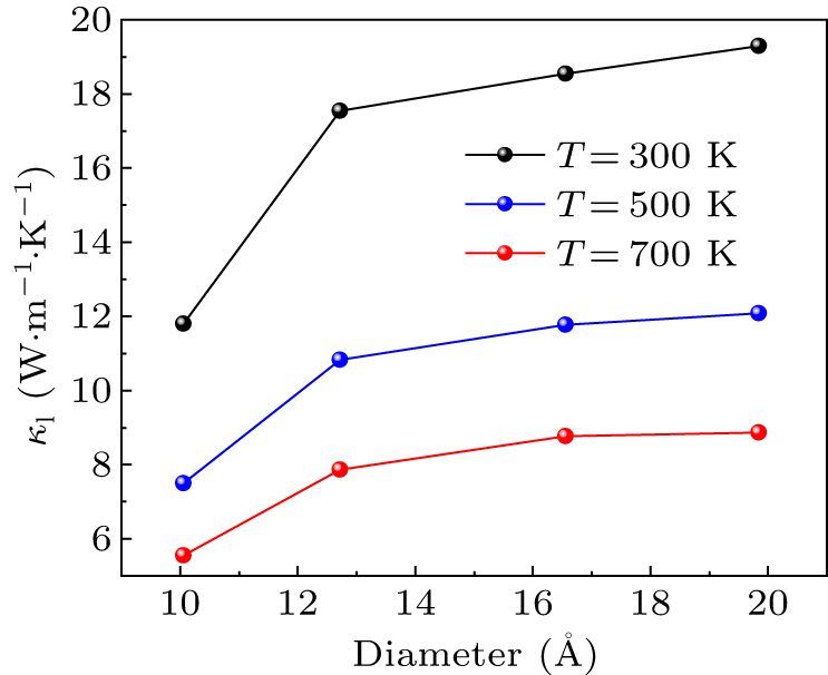
Fig. 6. Variation of lattice thermal conductivity with diameter at T = 300 K, 500 K, and 700 K.
Download figure:
Standard imageIn Fig. 7, the high-frequency phonon mode contribution of (ZnO)24 is evident, particularly in the two phonon DOS peaks near 350 cm−1 and 550 cm−1. The high-frequency phonon mode contribution of (ZnO)37 is significantly reduced compared with (ZnO)24, which accounts for the rapid increase in lattice thermal conductivity. In addition, the proportion of contributions from high-frequency phonon modes in (ZnO)54 and (ZnO)73 are more closely aligned with that in (ZnO)24, which slow down the growth rate in lattice thermal conductivity. In the case of thermal conductivity measurements for larger size ZnO nanowires, the thermal conductivity shows a linear increase with diameter.[43] In this work, the lattice thermal conductivity of ZnO nanowires shows a non-linear variation with diameter and the value of 12.72 Å seems to be an inflection point. When the diameter of ZnO nanowire is greater than 12.72 Å, the lower increment of lattice thermal conductivity with diameter can make a possible "sweet zone" for thermoelectric applications. As (ZnO)24 has the lowest lattice thermal conductivity of the four ZnO nanowires, the thermoelectric properties may also be prominent.
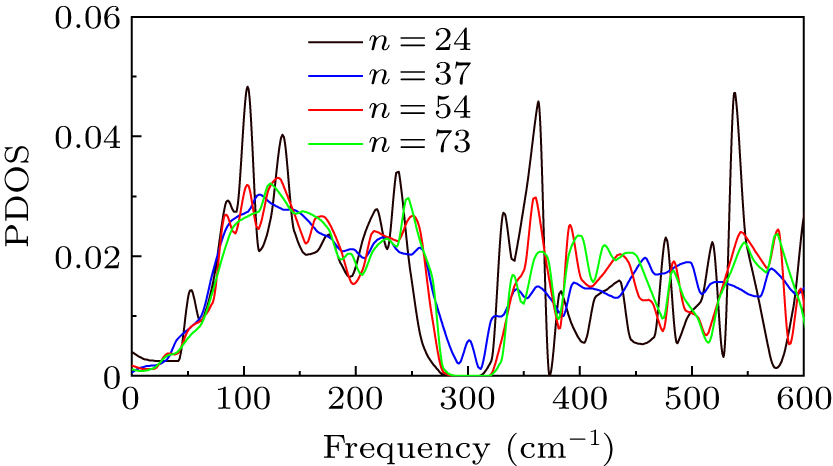
Fig. 7. Phonon DOS of (ZnO)24, (ZnO)37, (ZnO)54, and (ZnO)73.
Download figure:
Standard image3.4. Thermoelectric performance
In this section, the thermoelectric properties of ZnO nanowires are studied by combining the carrier transport properties with the lattice thermal conductivity properties. When calculating the ZT value, the total thermal conductivity including both electronic and lattice thermal conductivities is considered. The lattice thermal conductivity of ZnO nanowires is typically higher than the electronic thermal conductivity. Therefore, the gap between P-type and N-type electronic thermal conductivities will be reduced due to the contribution of lattice thermal conductivity, and the total thermal conductivity of P-type is about 1.27–2 times that of N-type (as shown in Fig. 8(a)).
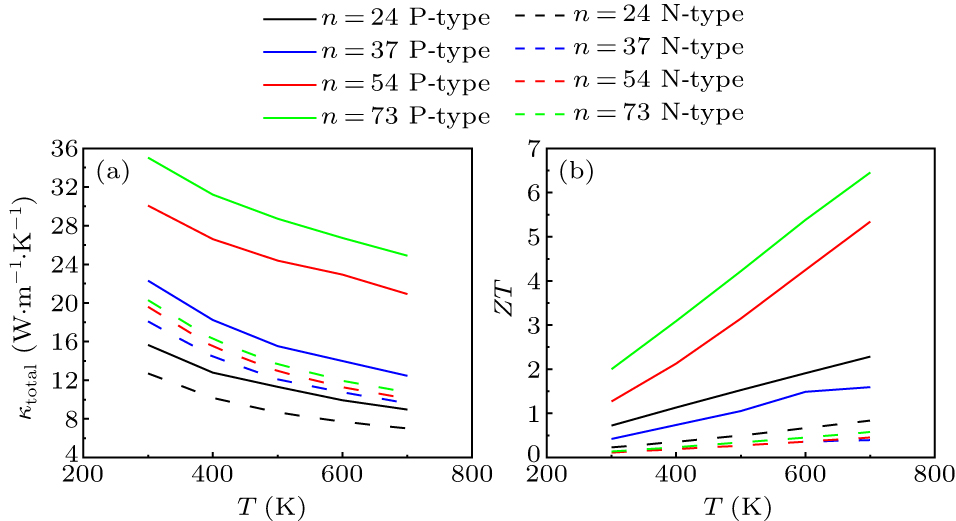
Fig. 8. (a) Total thermal conductivity and (b) ZT values of (ZnO)24, (ZnO)37, (ZnO)54, and (ZnO)73.
Download figure:
Standard imageAs the temperature rises, the lattice thermal conductivity continues to decline, but the decline rate gradually slows down and the contribution of electronic thermal conductivity to the total thermal conductivity becomes more important. Under the combined effect of the three parameters, the average ratio of ZT values of P-type to N-type is 7.75 (as shown in Fig. 8(b)). In addition, the energy band degeneracy effect is amplified at higher temperatures owing to the broadening of the Fermi distribution. The calculated P-type ZT value shows a distinct upward trend with temperature and reaches the highest value of 6.4 at 700 K for P-type (ZnO)73. As the diameter of the nanowire increases, more converging energy bands participate in the carrier transport at the VBM, and the slope of the P-type ZT with diameter becomes greater, which can be viewed in Fig. 9(a). In contrast, the upward trend of N-type ZT with temperature is mainly caused by the downward trend of thermal conductivity. However, note that although N-type ZT values are not as high as P-type, the achieved ZT values of 0.11–0.83 are still higher than the reported ones for ZnO-based thermoelectric materials.[44,45]

Fig. 9. The ZT values against diameter for (a) P-type and (b) N-type ZnO nanowires.
Download figure:
Standard imageNext, the variation of ZT value with the diameter of nanowires is further discussed. Intuitively, an increase in nanowire diameter implies an expansion of the conductive path, suggesting that the axial carrier transport of nanowires should increase monotonically with an increase of diameter. Based on the calculation results in Fig. 9, for the four configuration models in this work, the ZT from (ZnO)24 to (ZnO)37 does not rise but falls, while rises dramatically for (ZnO)54 and (ZnO)73. As mentioned in Subsection 3.2.4, the carrier transport capacity of (ZnO)37 does not show a significant improvement compared with (ZnO)24. In Subsection 3.3.2, it is also mentioned that (ZnO)37 exhibits a notable increase in lattice thermal conductivity, marking it as the turning point for lattice thermal conductivity with diameter variation. The combination of these two factors inevitably results in (ZnO)37 representing a point where the ZT value is relatively low. Additionally, there exists a distinct discrepancy in the pattern of ZT variation with diameter between P-type and N-type. It is observed that the highest ZT values for P-type occur at the largest diameter of (ZnO)73 while the highest ZT values for N-type at the smallest diameter of (ZnO)24. This phenomenon can be attributed to the fact that the P-type carrier transport capacity greatly surpasses that of the N-type and only the VBMs exhibit the energy band degeneracy effect with increasing size. The P-type ZT variation is dominated by the carrier transport capacity, while the N-type ZT variation is more influenced by the lattice thermal conductivity. Nevertheless, this explanation can only account for the differences in ZT variation trends between P-type and N-type ZnO nanowires. It does not yet fully clarify the overall pattern of ZT variation with diameter, especially the phenomenon of an inflection point at (ZnO)37. In Subsection 3.2.3, a turning point was observed in the deformation potential constant at (ZnO)37, which aligns with the variation pattern of ZT with diameter. Therefore, it can be inferred that there are some diameter-related factors influencing carrier transport.
The radial section of ZnO 〈0001〉 nanowires is composed of a hexagonal lattice, so the radial section of ZnO 〈0001〉 nanowires can also be viewed as a hexagon, which can be categorized into two types of configuration models, as shown in Fig. 10. One is a regular hexagon type represented by (ZnO)24 and (ZnO)54 and the number of hexagonal lattices involved in each side is the same. The other is a non-regular hexagon type represented by (ZnO)37 and (ZnO)73 and the hexagonal lattice number on adjacent sides differs by 1. Obviously, the regular hexagonal configuration is more symmetrical in the geometric spatial distribution. Figure 3 illustrates that the charge is distributed evenly around the atom surrounding the central axis in ZnO nanowires. The symmetry of charge distribution closely corresponds to the symmetry of atomic space distribution. This means that (ZnO)24 and (ZnO)54 with a regular hexagonal configuration exhibit strong symmetry, while (ZnO)37 and (ZnO)73 possess weaker symmetry due to their non-regular hexagonal configuration. This asymmetry influence on the deformation potential constant will diminish with the increasing nanowire diameter, as the proportion of the difference in the number of lattices between adjacent sides to the total number of lattices on a side becomes smaller. Exactly, the impact of asymmetry is significantly more pronounced on (ZnO)37 than on (ZnO)73. This provides an explanation for why the transport properties and thermoelectric properties of ZnO nanowires reach a minimum value at (ZnO)37 and then steadily increase with increasing diameter. Figure 9 clearly shows the variation of ZT values of ZnO nanowires with diameter. It is found that after the lowest ZT value at the diameter size of (ZnO)37, the ZT value goes higher with increasing diameter.
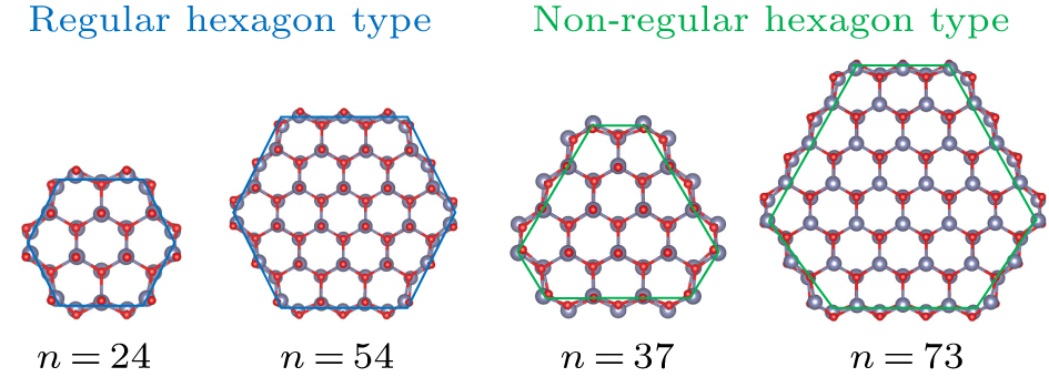
Fig. 10. Schematic of two geometric configuration models of ZnO nanowires.
Download figure:
Standard imageNote that the ZT value cannot rise indefinitely with diameter, as the thermal conductivity gradually enters a linear growth pattern as the diameter size increases, which can cause an unavoidable deteriorated effect on the ZT value. It is essential to emphasize that defects in the actual experimental samples result in lower ZT values compared with theoretical computations since ideal geometric models are usually used in the computations. As mentioned in this section, differences in configuration can influence the thermoelectric properties of ZnO nanowires. Defects in experimental samples can reduce the radial symmetry of the nanowires and constrain the transport of charge carriers within the nanowires, resulting in a decrease in thermoelectric performance.
The calculation results illustrate that the P-type ZnO nanowires have extremely strong carrier transport capabilities and the P-type (ZnO)73 can achieve a power factor over 1500 μW⋅cm−1⋅K−2, recording the highest ZT value of 6.4 at 700 K. It provides a theoretical basis for the application of ZnO nanowires in high-temperature scenarios in the future.
4. Conclusion and perspectives
In this study, we systematically investigated wurtzite-ZnO 〈0001〉 nanowires with four different diameters, by analyzing the geometrical configuration, thermal transport properties, carrier transport capacity and thermoelectric properties within a temperature range of 300 K–700 K based on deformation potential theory. The GGA + U method was employed in the study of ZnO nanowires for the first time to correct the underestimation of the band gap and thus accurately described the electronic structure of the material.
First, the ZnO nanowires were found to deliver an extremely high P-type carrier transport capacity originating from the band degeneracy effect of the multi-band VBM structure and the weak phonon–electron scattering effect. An ultra-high power factor over 1500 μW⋅cm−1⋅K−2 was achieved in P-type (ZnO)73 over a large temperature range. Then, a notable diameter-size dependence was observed in both the lattice thermal conductivity and the carrier transport capacity of ZnO nanowires with a mutual inflection point at 12.72 Å of (ZnO)37. For diameters larger than 12.72 Å, the thermal conductivity increases slightly, while the carrier transport capacity rises dramatically. On this basis, the highest ZT value of 6.4 is achieved for P-type (ZnO)73 at 700 K. Finally, two geometric configuration models of regular and non-regular hexagonal lattices for wurtzite-ZnO 〈0001〉 nanowires were introduced and their influences on the symmetry of geometry and charge distribution were discussed for the first time, which provided further evidence that (ZnO)37 is the inflection point of diameter for thermoelectric properties. This work demonstrates the crucial role of size control in improving the thermoelectric performance of ZnO nanowires and provides an outlook and guidance for practical material preparation and applications.
Acknowledgments
The numerical calculations in this work were done at the Hefei Advanced Computing Center. Project supported by the National Natural Science Foundation of China (Grant Nos. 52130604 and 51825604).