
Abstract
The realization of perpendicular magnetization and perpendicular exchange bias (PEB) in magnetic multilayers is important for the spintronic applications. NiO(t)/[Ni(4 nm)/Pt(1 nm)]2 multilayers with varying the NiO layer thickness t have been epitaxially deposited on SrTiO3 (001) substrates. Perpendicular magnetization can be achieved when t < 25 nm. Perpendicular magnetization originates from strong perpendicular magnetic anisotropy (PMA), mainly resulting from interfacial strain induced by the lattice mismatch between the Ni and Pt layers. The PMA energy constant decreases monotonically with increasing t, due to the weakening of Ni (001) orientation and a little degradation of the Ni–Pt interface. Furthermore, significant PEB can be observed though NiO layer has spin compensated (001) crystalline plane. The PEB field increases monotonically with increasing t, which is considered to result from the thickness dependent anisotropy of the NiO layer.
Export citation and abstract BibTeX RIS
1. Introduction
Perpendicular magnetization is essential for a wide range of technologies including spin transfer torque (STT) magnetic random access memory (MRAM), spin–orbit torque MRAM, ultrahigh-density magnetic recording devices, Racetrack memory, etc.[1–8] A ferromagnetic (FM) layer can be perpendicularly magnetized when it possesses a perpendicular magnetic anisotropy (PMA) overcoming its shape anisotropy. In general, PMA originates from interface and/or bulk magnetic anisotropy. In ordinary ferromagnetic/non-ferromagnetic (FM/NM) or FM/FM superlattices, e.g., Co/Pt,[9, 10] Co/Pd,[11, 12] CoFeB/MgO[13] and Co/Ni,[14] PMA results from the former and suffers from the extremely thin FM layer with its thickness in one nanometer scale. The PMA in the Ni-based epitaxial metallic superlattices (e.g., Ni/Cu (001)) mainly results from the strain effect caused by the lattice mismatch between Ni and the nonmagnetic layer (e.g., Cu).[15, 16] This interface-induced strain can propagate into the Ni layer and therefore the generated PMA is a kind of bulk magnetic anisotropy. Note that the strain-induced PMA results from the magnetoelastic effect for the FM layer. Very recently, Seki et al. reported that strain-induced PMA and perpendicular magnetization could be realized in epitaxial Ni/Pt (001) superlattices directly deposited on (001) SrTiO3 substrates, though the lattice constants for Ni and Pt are 3.52 Å and 3.93 Å, respectively.[17] They further reported that the anomalous Nernst coefficient for the perpendicularly magnetized Ni/Pt superlattice could be increased up to one order of magnitude larger than that for the bulk Ni.[18] Therefore, Ni/Pt superlattice is a promising material for spintronic and spin caloritronic applications. The obvious advantage of the strain-induced PMA system is the wide thickness range of the FM layer, which can even exceed ten nanometers,[15–17] making the fabrication much easier than that of the interface-induced PMA materials.
The interfacial interaction between FM and antiferromagnetic (AFM) layers leads to the so-called exchange bias (EB) effect, showing that the magnetic hysteresis (M–H) loop shifts along the magnetic field axis.[19, 20] Perpendicularly magnetized FM film exchange coupled with AFM layer can produce perpendicular exchange bias (PEB), which has promising applications in advanced spintronic devices and thus attracted much interest. For examples, PEB is much more desirable for high magnetic stability, low power consumption and ultrafast operation.[21, 22] PEB has been realized in multilayers with interface-induced PMA like Co/Pt, Co/Pd, Co/Ni superlattices coupled with an AFM layer such as IrMn, NiO,[21–24] which also suffers from much smaller FM layer thickness.
Perpendicularly magnetized Ni/Pt (001) superlattice could be epitaxially grown on the SrTiO3 (001) single-crystal substrate with a high PMA constant.[17] The PMA is mainly contributed by the strain-induced bulk effect and can be maintained with the Ni layer thickness up to 5 nm, providing us a good candidate to investigate PEB in bulk PMA system. NiO is a G-type AFM material owning relatively high Néel temperature (∼525 K) and crystallizes in rock-salt structure.[25] In addition, its lattice constant is 4.176 Å,[26] which differs not too much from that of SrTiO3 (3.905 Å).[17] These may lead to possible epitaxial growth of NiO layer and subsequent Ni/Pt superlattice on SrTiO3 (001) substrate, thus PEB might be established.
In this work, NiO (001) layer is directly grown on SrTiO3 (001) substrates, followed by epitaxial growth of a series of perpendicularly magnetized Ni/Pt (001) superlattices. Obvious PMA and PEB have been successfully achieved, and carefully investigated by varying the thickness of the NiO layer. The dependences of PMA and PEB on the NiO layer thickness can be understood based on the modification of Ni (001)-orientation and anisotropy of NiO layer.
2. Experimental details
The NiO(t)/[Ni(4.0/Pt(1.0)]N multilayers were deposited by magnetron sputtering on SrTiO3 (001) substrates. Here, t and N denote the NiO layer thickness and the period number of Ni/Pt superlattices, respectively. The value in the parentheses is in units of nanometer. The base pressure was below 5×10⁻⁶ Pa and Ar pressure was kept at 0.3 Pa during the film deposition. Prior to the deposition, the substrates were annealed at 400 °C for half an hour. First, the NiO layer was deposited directly on SrTiO3 substrate through a commercial NiO target by RF sputtering with t varying from 5 nm to 25 nm. Then, [Ni(4.0)/Pt(1.0)]N superlattice was deposited by DC sputtering. Note that the first layer of the [Ni/Pt]N superlattice is Ni, which is directly grown on the NiO layer. During the deposition of NiO layer and subsequent Ni/Pt superlattice, the substrate temperature was kept at 400 °C and meanwhile an external field of about 1500 Oe was applied perpendicular to the film plane. After that, the substrate was cooled down to room temperature and the magnetic field was still applied. Therefore PEB in NiO/[Ni/Pt]N multilayer can be established. The thicknesses of the Ni and Pt layers were fixed at 4.0 nm and 1.0 nm, respectively, to obtain significant PMA.[17] The period number N was chosen to be 2 due to that the strongest PEB was obtained experimentally, which is consistent with that the EB field generally decreases with increasing the FM layer thickness.[20] Finally, a 2.0-nm-thick Al layer was deposited at room temperature as a capping layer for preventing the multilayer from oxidation. The crystalline structures of the samples were characterized by x-ray diffraction (XRD, Bruker D8-Advance) with Cu Kα radiation (λ = 1.5406 Å). In addition, cross-sectional high-resolution transmission electron microscopy (HRTEM, FEI Titan G2 60-300) characterizations were performed to exhibit the microstructure. Both in-plane and out-of-plane M–H loops for all the samples were measured by a vibrating sample magnetometer (VSM, Microsense EV-7). The surface roughness was determined by atomic force microscopy (Veeco Dimension V). All the characterizations and measurements were carried out at room temperature.
3. Results and discussion
Figure 1(a) shows the XRD patterns for NiO(t)/[Ni/Pt]2 samples with t = 5, 10, 15, 20, 25 nm on single-crystal SrTiO3 (001) substrate. For comparison, the XRD pattern of the substrate is also shown. Besides the peaks from the SrTiO3 substrates, a strong NiO (002) peak can be observed clearly for the samples with t > 5 nm, suggesting the epitaxial growth of NiO layer on SrTiO3 (001) substrate. The enlarged XRD patterns displayed in Fig. 1(b) show a slight shift of the NiO (002) peak from 42.82° to 43.00° as t increases from 15 nm to 25 nm, reflecting that the out-of-plane lattice constant c of the NiO layer decreases monotonically from 4.220 Å to 4.202 Å, which is a little larger than the value of bulk NiO (4.176 Å). There is an obvious lattice mismatch (∼6.5%) between NiO and SrTiO3 since the lattice constant of SrTiO3 is only 3.905 Å. Therefore, when NiO film is epitaxially grown on SrTiO3 substrate with (001) orientation, a compressive strain is generated in the film plane, making the value of c increase accordingly. With increasing the NiO layer thickness, the in-plane strain is relaxed, leading to the gradual decrease of c.

Figure 1. (a) XRD patterns of NiO(t)/[Ni/Pt]2 samples with t = 5, 10, 15, 20, 25 nm and the bare SrTiO3 substrate. The asterisks denote the reflections from SrTiO3 (001) substrate. (b) The enlarged region with 2θ varied from 40° to 45° for all the NiO/[Ni/Pt]2 samples in (a). The red inverted triangles denote the peak positions for NiO (002).
Download figure:
Standard imageIn Fig. 1(a), it is noted that the Ni (002) peak can only be observed in the sample with t = 5 nm. This may be due to the small thickness (i.e., 8 nm) of the total Ni layers for N = 2. To verify this argument, three samples of NiO(5 nm)/[Ni(4 nm)/Pt(1 nm)]N with N = 2, 3, 4 were prepared and the corresponding XRD patterns are shown in Fig. 2(a). It demonstrates that the Ni (002) peak becomes more and more clear when N increases gradually from 2 to 4. Meanwhile, the satellite reflections also become more significant, indicating the sharp Ni–Pt interface with uniform layer thicknesses. In contrast, when the same Ni/Pt superlattices are directly deposited on SrTiO3 (001) substrates, the Ni (002) peaks and corresponding satellite reflections become even distinct, as shown in Fig. 2(b). These results indicate that the Ni/Pt superlattice grows with (001) orientation and sharp Ni-Pt interface on NiO (001) layer, while the (001)-orientation is weaker than that for the same superlattices deposited on SrTiO3 (001) substrates directly. Moreover, the absence of Pt (002) peak (2θ ∼ 46.2°) in Figs. 1 and 2 may be due to the small thickness as well or overlapping with the peaks from the SrTiO3 substrate. With further increasing the NiO layer thickness above 5 nm, Ni (002) peaks are absent in the XRD patterns for NiO(t)/[Ni/Pt]2 multilayers, which may be due to the mosaic structure[27] of Ni/Pt layers and will be discussed in the following.
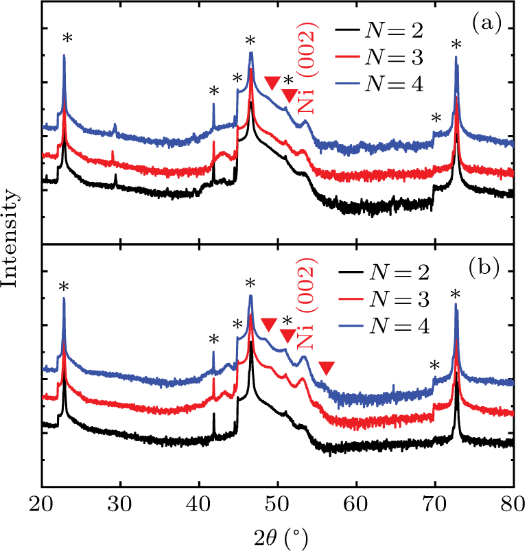
Figure 2. XRD patterns for the (a) SrTiO3/NiO(5.0)/[Ni(4.0)/Pt(1.0)]N and (b) SrTiO3/[Ni(4.0)/Pt(1.0)]N samples with the period number N = 2, 3, 4. The value in the parentheses is in units of nanometer. The asterisks denote the reflections from SrTiO3 (001) substrate. The red inverted triangles represent the satellite reflections of Ni (002) peaks.
Download figure:
Standard imageIn order to further investigate the growth mode for the multilayer film, cross-sectional HRTEM characterizations were performed on a representative sample with t = 20 nm and N = 2, and the corresponding images are shown in Fig. 3. As displayed in Fig. 3(a), followed by an initial ∼2 nm thick transition layer residing at the SrTiO3–NiO interface, very clear lattice can be observed in the NiO layer, unambiguously demonstrating the epitaxial growth of NiO layer. Calculated from the interplanar spacing in the NiO layer, the averaged lattice constants c (out-of-plane) and a (in-plane) are 4.199 Å and 4.082 Å, respectively. Thus, a compressive strain is generated in the film plane and thus the interplanar spacing in the out-of-plane direction increases, agreeing well with the XRD characterization results. As shown in Fig. 3(b), the lattice for the Ni and Pt layers can be clearly observed, indicating the epitaxial and coherent growth of Ni/Pt superlattice on the NiO layer with the preferred (001) orientation. In contrast to very clear and smooth interface of NiO–SrTiO3, the interface between NiO and the first Ni layer is relatively rough (see Fig. 3(a)) and even discontinuous in some locations (see Fig. 3(c)). These results indicate that the first Ni layer forms islands following the Volmer–Weber growth mode[28] due to the large lattice mismatch (∼15.7%) between Ni and NiO, which is much similar to the epitaxial growth of Ni layer on SrTiO3 (001) substrate.[17] The contrast due to the different electron scattering ability indicates that the subsequent Pt and Ni layers are continuous. From Fig. 3(b), the c (a) value of the Ni layer is calculated to be 3.510 Å (3.621 Å), which is slightly smaller (larger) than the bulk value (3.52 Å[17]), suggesting the existence of tensile strain in the film plane direction. This kind of strain is of great importance for inducing bulk PMA in the Ni/Pt superlattice.[17] In Fig. 3(d), the selected area electron diffraction (SAED) pattern displays two sets of diffraction spots scattered in square shape, one denotes SrTiO3 and the other belongs to NiO, which further confirms the epitaxial growth of NiO on SrTiO3 (001) substrate. Because both the Ni and Pt layers are very thin, the corresponding diffraction spots can hardly be distinguished. As indicated by the green lines in Fig. 3(b), the (001) lattice planes of the Ni layer on NiO layer, and following Ni and Pt layers are not exactly parallel to the substrate surface, but show some bending., i.e., mosaic structure.[27] Thus, the lattice planes cannot fully fulfill the Bragg diffraction conditions in XRD θ–2θ scan measurements, leading to the disappearance of the Ni (002) peaks in this sample.
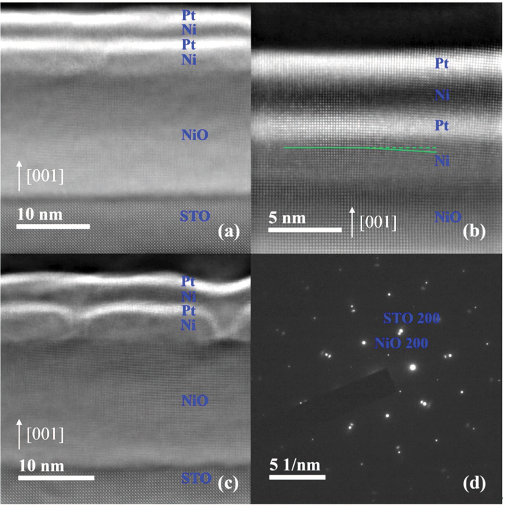
Figure 3. Cross-sectional HRTEM images for SrTiO3(STO)/NiO(20 nm)/[Ni(4 nm)/Pt(1 nm)]2/Al(2 nm) sample taken in two different locations for (a) and (c). (b) A magnified image for (a). (d) SAED image for the same sample. The solid and dash green lines in panel (b) are guides to eyes.
Download figure:
Standard imageFigure 4(a)–4(f) display the M–H loops for the NiO(t)/[Ni/Pt]2 samples with varying t from 0 to 25 nm. The blue and red curves denote the hysteresis loops measured by applying out-of-plane and in-plane magnetic fields, respectively. The positive direction of the measuring field for the out-of-plane M–H loop is the same as that of the applied field during film deposition. Note that H ranges from −6 kOe to 6 kOe for all the measurements except for measuring the in-plane M–H loop for the sample with t = 0 due to the very large saturate field. Thus, the maximum H is increased to 10 kOe to acquire a more trustable loop after removing the linear part at high field. However, to be in line with all the other loops, this loop is still plotted in the range between −6 kOe to 6 kOe, as shown in Fig. 4(a). Without NiO layer (t = 0), the [Ni/Pt]2 multilayer possesses out-of-plane easy axis with a very square M–H loop, reproducing well the results reported previously.[17] After the insertion of NiO layer, the easy axis can still be kept in the out-of-plane direction when t is less than 25 nm. However, the M–H loop becomes more slant and the Mr/Ms value decreases continuously, indicating a weakening tendency of PMA in the [Ni/Pt]2 superlattice. This is also consistent with the decreasing tendency for the in-plane saturation field as t is increased. When t equals to 25 nm, the in-plane and out-of-plane hysteresis loops are almost overlapped, indicating that the PMA is much weaker in this sample. Besides the appearance of PMA in the Ni/Pt superlattice, PEB can be also observed and varies significantly with changing the NiO layer thickness. As shown in the insets of Fig. 4, PEB becomes more and more prominent as t is increased. In contrast, the in-plane exchange bias can hardly be observed for all the samples.

Figure 4. The M–H loops for NiO(t)/[Ni/Pt]2 samples with t = 0, 5, 10, 15, 20 and 25 nm, respectively. The blue and red curves denote the hysteresis loops measured with out-of-plane and in-plane magnetic fields, respectively. The enlarged views for each out-of-plane loop with H varied from −0.4 kOe to 0.4 kOe are displayed in each inset.
Download figure:
Standard imageTo quantify the variation of PMA and PEB, the effective uniaxial magnetic anisotropy constant (Keff), the uniaxial magnetic anisotropy constant (Ku) and exchange bias field (HE) against the NiO layer thickness are summarized in Figs. 5(a)–5(c), respectively. Note that Ku reflects the intrinsic uniaxial magnetic anisotropy of the multilayer. Keff can be determined from the area enclosed between the out-of-plane and in-plane M–H loops as shown in Fig. 3, and positive (negative) value denotes that the easy axis is out-of-plane (in-plane). The values of Keff, saturation magnetization (Ms), and Ku comply with the relation  . Here,
  denotes the shape anisotropic energy which originates from the demagnetization energy along the film normal direction. As shown in Fig. 5(a), Keff first drops abruptly with inserting NiO layer, and then decreases gradually with further increasing t. Finally, Keff approaches zero when t equals to 25 nm. The value of Ku against t is plotted in Fig. 5(b), which shows a similar t dependence to that of Keff. A little fluctuation can be observed in the Ku–t curve around t = 15 nm, which is due to the fluctuation of the value of Ms. When a 5 nm NiO layer is inserted between the Ni layer and SrTiO3 substrate, the Ni (001)-orientation weakens significantly, which can be seen by comparing the strength of Ni (002) XRD peaks shown in Figs. 2(a) and 2(b). On the other hand, the XRD satellite reflections corresponding to the Ni (002) peak are more significant in the SrTiO3/[Ni/Pt]N
multilayers in comparison with those in the SrTiO3/NiO/[Ni/Pt]N
multilayers, indicating that the Ni–Pt interface becomes relatively worse in the latter. The weakening of Ni (001)-orientation and degradation of Ni–Pt interface after insertion of the NiO layer are both resulted from the mosaic structure of the Ni/Pt layers, which has been verified by the HRTEM images shown in Fig. 3(b). Because bulk single-crystal Ni has the largest magnetostrictive coefficient along (001) direction[29, 30] and the PMA in Ni/Pt multilayer originates from the Ni–Pt interfacial strain, it is reasonable to observe a significant reduction of Ku and Keff with insertion of a thin NiO layer and a continuous decrease with further increasing t. Moreover, as shown in the inset of Fig. 5(a), the peak-to-peak surface roughness (Ra) for the NiO layer increases monotonically from 0.078 nm to 0.117 nm with t increased from 5 nm to 25 nm. The roughness data were obtained by the atomic force microscopy characterization performed on a series of NiO single layer films prepared under the same conditions as those for the present NiO/[Ni/Pt]2 multilayers. These two reasons may cause a gradual decrease of Keff after t exceeds 5 nm. Since the value of Ra is very small, it is reasonable to consider that the weakening of Ni (001)-orientation and degradation of Ni–Pt interface after insertion of the NiO layer play the dominant role in determining the t dependence of Ku or Keff.
denotes the shape anisotropic energy which originates from the demagnetization energy along the film normal direction. As shown in Fig. 5(a), Keff first drops abruptly with inserting NiO layer, and then decreases gradually with further increasing t. Finally, Keff approaches zero when t equals to 25 nm. The value of Ku against t is plotted in Fig. 5(b), which shows a similar t dependence to that of Keff. A little fluctuation can be observed in the Ku–t curve around t = 15 nm, which is due to the fluctuation of the value of Ms. When a 5 nm NiO layer is inserted between the Ni layer and SrTiO3 substrate, the Ni (001)-orientation weakens significantly, which can be seen by comparing the strength of Ni (002) XRD peaks shown in Figs. 2(a) and 2(b). On the other hand, the XRD satellite reflections corresponding to the Ni (002) peak are more significant in the SrTiO3/[Ni/Pt]N
multilayers in comparison with those in the SrTiO3/NiO/[Ni/Pt]N
multilayers, indicating that the Ni–Pt interface becomes relatively worse in the latter. The weakening of Ni (001)-orientation and degradation of Ni–Pt interface after insertion of the NiO layer are both resulted from the mosaic structure of the Ni/Pt layers, which has been verified by the HRTEM images shown in Fig. 3(b). Because bulk single-crystal Ni has the largest magnetostrictive coefficient along (001) direction[29, 30] and the PMA in Ni/Pt multilayer originates from the Ni–Pt interfacial strain, it is reasonable to observe a significant reduction of Ku and Keff with insertion of a thin NiO layer and a continuous decrease with further increasing t. Moreover, as shown in the inset of Fig. 5(a), the peak-to-peak surface roughness (Ra) for the NiO layer increases monotonically from 0.078 nm to 0.117 nm with t increased from 5 nm to 25 nm. The roughness data were obtained by the atomic force microscopy characterization performed on a series of NiO single layer films prepared under the same conditions as those for the present NiO/[Ni/Pt]2 multilayers. These two reasons may cause a gradual decrease of Keff after t exceeds 5 nm. Since the value of Ra is very small, it is reasonable to consider that the weakening of Ni (001)-orientation and degradation of Ni–Pt interface after insertion of the NiO layer play the dominant role in determining the t dependence of Ku or Keff.
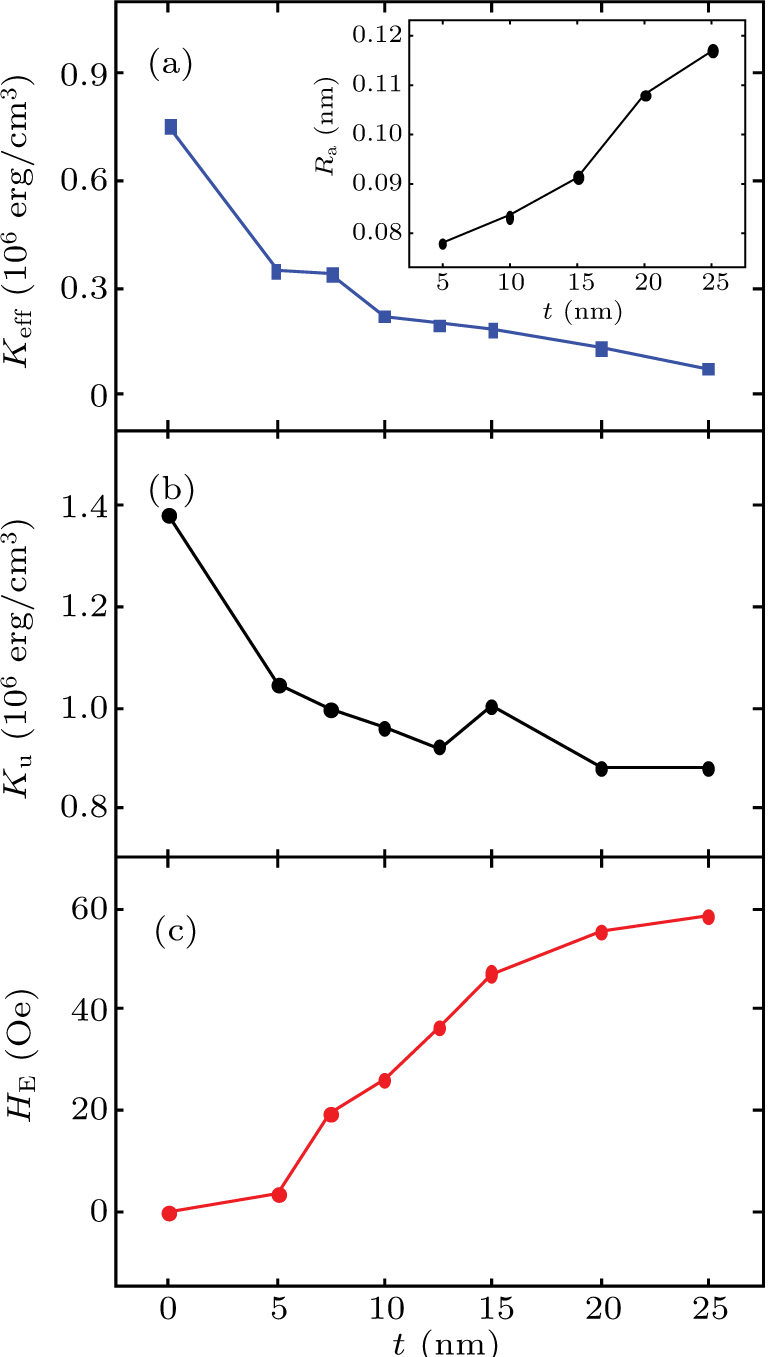
Figure 5. (a) The effective uniaxial magnetic anisotropy constant (Keff), (b) the uniaxial magnetic anisotropy constant (Ku) and (c) the perpendicular exchange bias field (HE) against the NiO layer thickness. The inset of (a) denotes the surface roughness against the NiO layer thickness on a series of NiO single layer films.
Download figure:
Standard imageThe value of HE can be calculated by HE = − (HL + HR)/2, where HL and HR are the coercive fields of the left and right branches for the out-of-plane M–H loop, respectively. As displayed in Fig. 5(c), only a trivial HE of about 3 Oe appears when t equals to 5 nm. Then, HE increases monotonically with increasing t and reaches about 60 Oe when t is 25 nm. In the present work, NiO (001) layer could be well epitaxially grown on SrTiO3 (001) substrate, which has been verified by the XRD and TEM studies. It is well accepted that an ideal NiO (001)-plane is spin compensated,[31–33] hence only weak EB effect could be observed at room temperature, as reported in some FM/(001)-NiO bilayer films with the FM magnetization in the film plane.[31, 32, 34] Furthermore, it is noted that PEB has never been reported in (001)-NiO pinning systems. The generation of PEB in the present NiO/[Ni/Pt]2 multilayers is considered to result from the NiO–Ni interfacial fluctuation/roughness in terms of random field model.[35] According to this model, interfacial fluctuation/roughness between NiO and Ni layers may generate random magnetic fields, which are produced by isolated FM spins penetrating into the AFM layer to form uncompensated surface.[35] They act on the interfacial spins and induce an out-of-plane unidirectional anisotropy, i.e., PEB consequently. As for the variation of PEB against t, it may be resulted from the thickness dependent anisotropy energy of NiO. The variation of HE with the AFM layer thickness is generally explained by competition between the interfacial exchange energy and the anisotropy energy of the AFM layer.[36] Generally, with increasing AFM thickness in exchange biased AFM/FM bilayers, HE often appears at a certain thickness and then increases to a maximum at a critical thickness. After that, HE may keep almost unchanged[37, 38] or decrease slowly with further increasing the AFM layer thickness.[36, 39] For the NiO-based EB bilayers, the critical thickness is often in the range between 30 nm and 40 nm.[36, 40, 41] For the present studies, since the maximum thickness of the NiO layer is only 25 nm, it is reasonable to observe a monotonic increase of HE against t.
4. Conclusions
In summary, we have obtained (001)-oriented epitaxial growth for a series of NiO(t)/[Ni(4 nm)/Pt(1 nm)]2 multilayers deposited on SrTiO3 (001) substrates with varying t from 0 to 25 nm. PMA is realized to overcome the shape anisotropy, leading to perpendicularly magnetized Ni/Pt superlattice. Although an ideal NiO (001)-plane is spin compensated, obvious PEB can still be observed in the present NiO-pinning [Ni/Pt]2 multilayers, which can be understood in terms of the random field model. Furthermore, the PEB field can be further enhanced to a maximum value of about 60 Oe with increasing t up to 25 nm. These findings will provide new clues for developing strain-induced bulk PMA and PEB materials for spintronic applications.
Acknowledgments
Project supported by the National Natural Science Foundation of China (Grant Nos. 51971109, 51771053, 52001169, and 11874199), the National Key Research and Development Program of China (Grant No. 2016YFA0300803), the Fundamental Research Funds for the Central University, China (Grant No. 2242020k30039), and the open research fund of Key Laboratory of MEMS of Ministry of Education, Southeast University.