
Abstract
Two-dimensional monolayer copper selenide (CuSe) has been epitaxially grown and predicted to host the Dirac nodal line fermion (DNLF). However, the metallic state of monolayer CuSe inhibits the potential application of nanoelectronic devices in which a band gap is needed to realize on/off properties. Here, we engineer the band structure of monolayer CuSe which is an analogue of a p-doped system via external atomic modification in an effort to realize the semiconducting state. We find that the H and Li modified monolayer CuSe shifts the energy band and opens an energy gap around the Fermi level. Interestingly, both the atomic and electronic structures of monolayer CuHSe and CuLiSe are very different. The H atoms bind on top of Se atoms of monolayer CuSe with Se–H polar covalent bonds, annihilating the DNLF band of monolayer CuSe dominated by Se orbitals. In contrast, Li atoms prefer to adsorb at the hexagonal center of CuSe, preserving the DNLF band of monolayer CuSe dominated by Se orbitals, but opening band gaps due to a slight buckling of the CuSe layer. The realization of metal-to-semiconductor transition from monolayer CuSe to CuXSe (X = H, Li) as revealed by first-principles calculations makes it possible to use CuSe in future electronic devices.
Export citation and abstract BibTeX RIS
1. Introduction
Two-dimensional (2D) materials with graphene-like one-atomic-thick honeycomb structures have attracted tremendous attention due to their novel properties and potential applications.[1–6] Recently, a new honeycomb analogue of graphene, monolayer transition metal selenide (CuSe), has been successfully fabricated on Cu(111) surfaces with or without intrinsically patterned triangular holes.[7,8] First-principles calculations based on a freestanding monolayer of CuSe predict that planar CuSe with a honeycomb lattice is thermodynamically stable and possesses two 2D Dirac nodal line fermions (DNLFs).[8] However, monolayer CuSe is not suitable for potential applications in electronic devices because of its metallic nature. A semiconducting feature is necessary for applications of CuSe in electronic devices. We notice that there are several Dirac points near the Fermi level. In addition, there is a prominent band gap which is only ∼ 1 eV above the Fermi level. On this basis we deduce that either the opening of a band gap or suitable doping of monolayer CuSe can make it a semiconductor.
The successful methods to alter the band structures of graphene-like 2D materials include controlling the thickness or the stacking geometry of 2D materials,[9–11] quantum confinement of charge carriers from 2D to 1D nanoribbons or nanotubes,[12–16] chemical doping,[17–19] strain,[20–23] and atomic modification.[24–26] First-principles calculations show that the band structure of monolayer CuSe has a gap above the Fermi level. A simple analysis of electron and band counting shows that monolayer CuSe is a p-type system with one electron depleted, indicating that modification by electron-donating atoms may lift the Fermi level toward the existing gap.
In this paper, we study influence of a modification via H and Li atoms on the band structure of monolayer CuSe, forming a new monolayer CuXSe (X = H, Li) These monolayers are dynamically stable, as evidenced by the calculated phonon dispersion. It is found that monolayer CuXSe (X = H, Li) does achieve the semiconducting state. Furthermore, monolayer CuHSe and CuLiSe are different in both atomic and electronic structures. For monolayer CuHSe, H atoms bind on top of Se atoms of monolayer CuSe with Se–H polar covalent bonds, annihilating the DNLF band of monolayer CuSe dominated by Se pz orbitals. In contrast, Li atoms prefer to adsorb at the hexagonal center of CuSe, preserving the DNLF band.
2. Calculation method
First-principles calculations were performed using the Vienna ab initio simulation package (VASP).[27,28] The local density approximation (LDA)[29] is used for exchange and correlation functional. The rotationally invariant LDA + U formalism proposed by Dudarev et al. is used[30] and Ueff is chosen as 6.52 eV for Cu.[31] The electronic wavefunctions are expanded in a plane wave basis set with an energy cutoff of 450 eV. For all the structures, a 15 Å vacuum layer is used. All atoms are fully relaxed until the residual forces on each atom are smaller than 10−3 eV/Å. The k-points sampling is 39 × 39 × 1. The phonon dispersion is calculated based on a 6 × 6 supercell using the finite displacement method as implemented in the PHONOPY package.[32–34]
3. Results and discussion
The relaxed monolayer CuSe possesses a graphene-like planar honeycomb structure, as shown in Fig. 1(a). Figure 1(b) shows the calculated electron localization function (ELF) indicating the degree of electron localization which allows to analyze the bonding character. We plot the ELF map in the vertical plane marked by the black dotted line in Fig. 1(a). It is found that there is only a little electronic localization between Cu and Se, while localized electrons are mainly distributed around Se, showing both covalent and ionic characters. To visualize the above picture, we further calculate the differential charge density and perform the Bader charge analysis. On the one hand, differential charge density (see Fig. 1(c)) clearly shows charge accumulations between Cu and Se atoms, while charge depletion on Cu and Se atoms, hence demonstrating a covalent bonding character. On the other hand, the Bader charge analysis indicates a 0.23 | e| charge transfer from a Cu atom to a Se atom, showing the evidence of ionic bonding.

Fig. 1. Atomic and electronic structures of monolayer CuSe. (a) Top and side views. (b)–(c) Cross sections of electron localization function and differential charge density, respectively. These cross sections are of the vertical plane marked by the black dotted line in (a), cutting through one Cu atom and one Se atom. (d) Band structure. The path for plotting band structures is marked in the inset. (e)–(f) Projected density of states on Cu and Se, respectively.
Download figure:
Standard imageTo better understand the electronic properties of monolayer CuSe, we calculate the band structure (see Fig. 1(d)) and projected density of states (PDOS) of monolayer CuSe (see Figs. 1(e) and 1(f)). Monolayer CuSe is intrinsically metallic with a gap region of 2.41 eV above the Fermi level marked in light blue in Fig. 1(d). Below the gap region, the three bands crossing the Fermi level can be classified into two groups.[8] The two downward hole-like bands are composed of the in-plane Se/orbitals and Cu/orbitals. These two bands are energetically degenerate at the Γ point arising from three-fold rotational symmetry. The upward electron-like band is composed of the out-of-plane Se and Cu/orbitals. From the PDOS, the band of upward dome marked by blue dotted curve in Fig. 1(d) is dominated by the out-of-plane Se pz orbital, which determines the bonding configuration for external atoms as shown below.
From the band structure, it is obvious that the Fermi level will shift to the gap region by electron doping. Considering that there are 17 valence electrons (Cu 3d104s1 and Se 4s24p4) with nine bands (see Fig. 1(d)) below the gap region in one CuSe unitcell, it is possible to move the Fermi level into the gap region by adding one electron to a CuSe unitcell resulting in a CuSe layer with a semiconducting character. Therefore, elements with one valence electron, for example, H and Li, can be expected to modify the electronic structure of monolayer CuSe.
The newly formed monolayer CuHSe and CuLiSe have different atomic configurations as shown in Fig. 2. H atoms prefer to adsorb on top of Se atoms, while Li atoms prefer to adsorb at the hexagonal center of monolayer CuSe. As reported in the previous work,[8] the planar monolayer CuSe is dynamically stable while the buckled one is not. After the atomic modification, the basal plane of CuSe is slightly buckled. Surprisingly, the phonon dispersion of monolayer CuHSe and CuLiSe with slightly buckled CuSe plane do not show imaginary frequency modes in the whole brillouin zone indicating the important role of atomic adsorption on the stabilization of the monolayer CuHSe and CuLiSe.
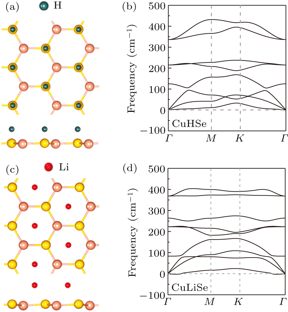
Fig. 2. Atomic structure and stability of monolayer CuHSe and CuLiSe. (a) Top and side views of CuHSe. (b) Phonon dispersion of monolayer CuHSe. (c) Top and side views of CuLiSe. (d) Phonon dispersion of monolayer CuLiSe.
Download figure:
Standard imageThe band structures of monolayer CuHSe and CuLiSe are presented in Figs. 3(a) and 3(b), respectively. Compared with the band structure of pristine CuSe (see Fig. 1(d)), the Fermi levels of monolayer CuHSe and CuLiSe shift up into the gap region transforming the monolayers to direct semiconductors, in agreement with our previous electron counting analysis. The band gaps of CuHSe and CuLiSe are 1.43 eV and 1.51 eV, respectively, which are smaller than the gap region of 2.41 eV in pristine CuSe. To confirm the band structure evolutions of monolayer CuHSe and CuLiSe, we calculate their band structures using the HSE06 hybrid functional as shown in Figs. 3(c) and 3(d), which is known to perform well for band structures and band gaps. The band gaps of CuHSe and CuLiSe are 2.08 eV and 1.98 eV, respectively, which are slightly larger than those obtained using LDA + U.
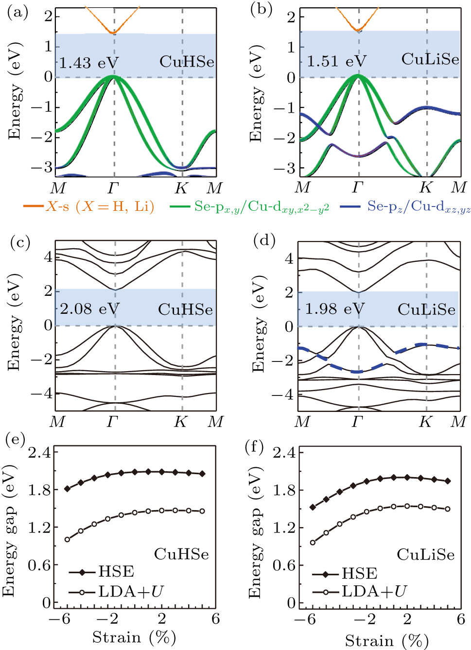
Fig. 3. Band structures at LDA + U level of monolayer (a) CuHSe and (b) CuLiSe, respectively. Band structures at HSE06 level of monolayer (c) CuHSe and (d) CuLiSe, respectively. Band gap variations with strain of monolayer (e) CuHSe and (f) CuLiSe, respectively.
Download figure:
Standard imageSince the growth of 2D materials on substrates is often accompanied by strain,[35,36] we further investigate the atomic and electronic properties of monolayer CuHSe and CuLiSe with different strains. The biaxial strain is applied via changing the lattice parameters of the monolayers and then fully relaxing the atomic positions. We find that the most stable adsorption sites of H and Li on CuSe do not change with increasing tensile and compressive strains. The band gap dependence on the strain has been calculated as shown in Figs. 3(e)–3(f), respectively. The band gaps of monolayer CuHSe and CuLiSe are both insensitive to tensile strain, while they decrease with compressive strains. When –5% compressive strain is applied, the band gap changes of monolayer CuHSe and CuLiSe are ∼ 0.2 eV and ∼ 0.4 eV, respectively.
It is interesting to note that CuHSe and CuLiSe show a different variation of the electronic band dispersion. CuLiSe has an electron-pocket-like band of upward dome near –2 eV as shown in Figs. 3(b) and 3(d), while CuHSe does not. Since this band is mainly dominated by the Se orbital, while H atoms prefer to adsorb on top of Se atoms, the missing of the electron-pocket-like band is due to the strong coupling between the Se orbital and the H s orbital.
To verify the above picture, we calculate the ELF, PDOS, and partial charge density of monolayer CuHSe shown in Fig. 4. The ELF (see Fig. 4(a)) clearly shows that a typical polar covalent bonding feature appears between the Se and H atoms, indicating the formation of a Se–H polar covalent bond. From the PDOS (see Fig. 4(b)), we can clearly see that the energy position of the Se orbital is consistent with that of the H s orbital indicating a hybridized bonding character. The bonding and antibonding states of the Se orbital and the H s orbital are marked by red arrows, which is confirmed by the partial charge density of these two peaks (from left to right), as shown in Figs. 4(c) and 4(d), respectively.
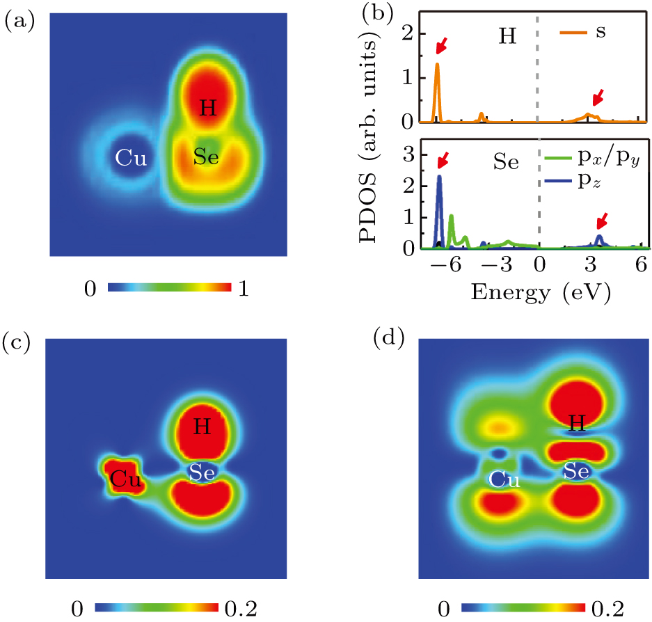
Fig. 4. Electronic properties of monolayer CuHSe. (a) Cross section of electron localization function. (b) Projected density of states on H and Se. [(c), (d)] Cross sections of partial charge density of the two peaks (from left to right) marked by red arrows in (b), respectively. These cross sections are of the vertical plane cutting through one Cu atom, one H atom and one Se atom.
Download figure:
Standard imageDue to the different intrinsic properties of H and Li, the atomic configurations and band structures of CuHSe and CuLiSe are different. H is a non-metallic element while Li is a metallic one. Therefore, H atoms prefer to adsorb on top of Se atoms, forming polar covalent bonds. The formation of covalent bonds between the Se and the H s makes the DNLF band of monolayer CuSe dominated by the Se orbitals disappear, forming a bonding state at a lower energy level and an antibonding state at a higher energy level. Li atoms prefer to adsorb at the hexagonal center of monolayer CuSe, preserving the DNLF band of monolayer CuSe dominated by the Se orbitals. However, due to the Li modification, the basal plane of CuSe is slightly buckled, opening band gaps of DNLFs.
4. Conclusion
In summary, the band structure of monolayer CuSe is engineered from metal to semiconductor via H and Li modification. The newly formed monolayer CuHSe and CuLiSe have different atomic configurations and band structures. H atoms bind on top of Se atoms of monolayer CuSe, while Li atoms prefer to adsorb at the hexagonal center of CuSe. CuLiSe has an electron-pocket-like band of upward dome near –2 eV, while CuHSe does not have due to the formation of the bonding and antibonding states of the Se orbital and the H s orbital. The realization of metal-to-semiconductor transition from monolayer CuSe to CuXSe (X = H, Li) as revealed by first-principles calculations makes the use of CuSe in electronic devices possible.
Acknowledgments
A portion of the research was performed in CAS Key Laboratory of Vacuum Physics. Computational resources were provided by the National Supercomputing Center in Tianjin.
Footnotes
- *
Project supported by the National Key Research & Development Projects of China (Grant No. 2016YFA0202300), the National Natural Science Foundation of China (Grant No. 61888102), and the Strategic Priority Research Program of Chinese Academy of Sciences (Grant No. XDB30000000).