


Abstract
In this work, we studied the photovoltage response of an antidot lattice to microwave radiation for different antidot parameters. The study was carried out in a Si/SiGe heterostructure by illuminating the antidot lattice with linearly polarized microwaves and recording the polarity of induced photovoltage for different angles of incidence. Our study revealed that with increased antidot density and etching depth, the polarity of induced photovoltage changed when the angle of incidence was rotated 90 degrees. In samples with large antidot density and/or a deeply etched antidot lattice, scattering was dominated by electron interaction with the asymmetrical potential created by semicircular antidots. The strong electron–electron interaction prevailed in other cases. Our study provides insight into the mechanism of interaction between microwaves and electrons in an antidot lattice, which is the key for developing an innovative ratchet-based device. Moreover, we present an original and fundamental example of antidot lattice etching through the use of a two-dimensional electron gas. This system deals with a hole lattice instead of an electron depletion in the antidot lattice region.
Export citation and abstract BibTeX RIS

Content from this work may be used under the terms of the Creative Commons Attribution-NonCommercial-ShareAlike 3.0 licence. Any further distribution of this work must maintain attribution to the author(s) and the title of the work, journal citation and DOI.
1. Introduction
In systems without spatial inversion symmetry such as macroporous silicon membranes [1], microfluidic channels [2], and vortexes in Josephson junction arrays [3], the directed motion of particles can be induced by a time-varying force. This directed motion, which is commonly referred to as the ratchet effect, is generated by the anisotropy of collision events. Such anisotropic collision events can be artificially realized by constructing asymmetric scatterers such as semidisks and cuts [4–9]. In our study, we patterned a semi-circular antidot array in a Si/SiGe heterostructure to create asymmetric scattering potential for a two-dimensional electron gas (2DEG) as shown in figure 1(b).

Figure 1. (a) Si/SiGe heterostructure schematic and different etching depth representation of samples studied (b) On left: representation of sample. Hall bar 4.5 mm long and Hall bar 50 μm wide. On right: representation of central part of Hall bar. Antidot lattice patterned in central part of Hall bar 230 μm long. Hexagonal symmetry of lattice is represented; side of hexagon is equal to lattice period a. Electrical measurements of antidot lattice part were made by using Hall probes 1, 2, 3, and 4. Semi-disk axis also indicated on right (for which θ = 0 degree). Electric field pointing vector of microwave for perpendicular polarization (θ = 90 degree) is represented in blue in lattice. Resulting electron flow is shown by arrows on each antidot. (c) Representation of microwave polarization orientation as function of semi disk axis. Electron flow for each polarization also indicated. Angle theta as function of antidot lattice orientation (semi disk axis) is shown.
Download figure:
Standard image High-resolution imageThe electronic version of the ratchet effect can be described as the capability of an asymmetric system to generate a directed transport under polarized microwave radiation. We focused on the ratchet effect originating from an antidot lattice patterned on a semiconductor heterostructure; see figure 1(a). As shown in figure 1(c), the carriers in the two-dimensional electron gas interact strongly with the asymmetrical potential induced by the antidots under microwave (MW) radiation, and the broken spatial symmetry forces the carriers to move preferably in one direction (ratchet effect), thereby generating a longitudinal photovoltage (semicircular antidot orientation). The semicircular antidots act as asymmetrical scatterers, which deflect carriers preferentially toward a particular direction and thereby generate a dc voltage. Since the voltage is generated by a current induced by the microwave radiation, the method can be used without an external electrical power source or any other electronic circuitry.
Figures 1(b) and (c) provide a clear picture of the Hall bar geometry and directional dependence of the polarity of the ratchet photovoltage. When the microwave polarization is oriented perpendicularly to the semi-disk axis (polarization angle is θ = 90 degrees), the electrons move towards the right side of the sample. When the microwave polarization is oriented parallel to the semi-disk axis (polarization angle is θ = 0 degrees), the electron flow direction is reversed; that is, the electrons move in the opposite direction, towards the left side of the sample. Longitudinal photovoltage induced by the ratchet effect can be measured by using Hall probes 1–2 and 3–4 fabricated on either side of the ratchet cell. According to theoretical estimates [7–9], the polarity of the ratchet photovoltage should change on changing the microwave polarization from 90 to 0 degrees for weak electron–electron (e–e) interaction. In contrast, with strong e–e interaction, the polarity of the ratchet–photovoltage will not change on rotating the angle of polarization, and discovering this fact is one of the important experimental results of this work.
Nanoscale devices based on the ratchet effect have attracted great scientific attention due to their unique ability to function without any power supply. Recently, ratchet-based wireless microwave detectors and current generators were successfully demonstrated in a Si/SiGe heterostructure, which paved the way for information technology development [17]. However, more ground work needs to be done to understand the dynamics of electron motion in antidot lattices, which will enable us to improve the performance of the devices quite substantially. In this work, we studied the interaction of microwaves with different antidot lattices etched on a Si/SiGe heterostructure.
The influence of a circular antidot lattice on 2DEG has been studied and reported elsewhere [10–13]. In the weak magnetic field regime, electrons describe circular motions around one or many antidots. This phenomenon localizes electrons and induces resistance change at low magnetic fields. The resulting resistance peaks are called commensurability peaks. From the peak position in magnetic fields, it is possible to extract the lattice period, which is the most common phenomenon observed on such structures. In our study, we focused our attention on semicircular antidot lattices—a very challenging geometry to achieve with existing lithographic tools. We intentionally chose this geometry because we wanted to see if we could create asymmetric scattering potential, which is the basis for realizing the ratchet effect.
The semicircular antidot lattice has been patterned and studied on a GaAlAs/GaAs and Si/SiGe heterostructures [14–16]. We chose the latter for our study because applications in wireless communication are possible with silicon-based materials commonly used for high-frequency devices [17]. A photovoltage amplitude of about 2 to 4 mV for Si/SiGe heterostructures and around 10 mV for GaAlAs/GaAs heterostructures was measured at 4 K. The signal was observed up to 80 K. At higher temperatures, the photovoltage disappears because the mobility of the 2DEG layer decreases, as does the depletion of electrons in the antidot lattice. As the mobility of 2DEG decreases, the mean free path becomes less than the period of the antidot lattice. In this scenario, the electrostatic scattering potential created by the antidot lattice is significantly reduced, thereby quenching the ratchet effect.
To increase the temperature limit and amplitude of the photovoltage, antidot lattice parameters such as the antidot radius, period, and etching depth should be tuned. The ratchet effect occurs when the electrons interact with the asymmetrical potential of the antidots. To optimize the ratchet photovoltage intensity, the antidot lattice parameters must be adjusted. Ideally, the antidot lattice period should be less than or equal to the mean free path [7–9, 14, 15] so that electrons move on a ballistic trajectory between two adjacent antidots. This implies that the antidot radius and period must be adjusted as a function of 2DEG mobility. For practical applications, observation of the ratchet effect at ambient temperature is very crucial. It implies that antidots should be able to maintain their asymmetric potential profile even at high temperature. To achieve this, the antidot lattice should be fabricated by a proper combination of different antidot parameters that maintains the depletion process even at high temperature. Moreover, the ratchet photovoltage response as a function of the microwave polarization orientation has to be established.
Operating this device requires no external electrical power source or other electronic circuitry such as an antenna. Because a ratchet cell is sensitive to a microwave power of a few μW, the ratchet cell can be seen as a nanoantenna. However, the ratchet cell is usually seen as a nanogenerator of current and voltage because the principle behind the effect is the induction of a directional electron motion. We have also demonstrated that the ratchet-based device can be used as a demodulator [17] for a theoretical carrier frequency ranging from 10 GHz to 10 THz [7].
This paper is organized into two parts. First, we present our analysis of magnetotransport properties. The commensurability peaks study gives information on the motion of electrons in the antidot lattice region. Second, we investigate the influence of antidot lattice parameters on the polarity of induced photovoltage for different microwave polarization orientations.
2. Experimental set-up
Photovoltage and magnetotransport experiments were performed at 4 K and in a low magnetic field by using the technique illustrated in previous works [14–16]. The samples were studied under a perpendicular magnetic field. The microwave system is made of a circular waveguide 5 m long with two transition pieces, which ensures that there is a rectangular window to the circular port connection at each end of the waveguide. The rectangular window controls the MW linear polarization on the sample [15].
A backward wave oscillator (BWO) generates a microwave power of 5 mW (measured at the waveguide output), leading to a power absorption of 3.6 μW by the antidot lattice fabricated over an area of 11 500 μm2. This low power absorption is sufficient to observe a large ratchet photovoltage. The microwave power at the waveguide output varies with the frequency, which can be tuned from 33 GHz to 50 GHz. Because the ratchet photovoltage amplitude is sensitive to the power [14], the measurements were made at maximum power, which led to an absorption power of a few μW by the ratchet cell. The incidence angle of polarized MW was changed by rotating the sample holder. The experimental uncertainty on the polarization angle was about ±10 degrees.
3. Sample description
The schematics of the samples used in this study are given in figure 1 and elsewhere [14–16]. Samples with different antidot radii and geometries (hexagonal and linear) were prepared by using conventional electron beam lithography (EBL) techniques. The samples were first cleaned by using an O2 descum plasma process and spin coated with a 1:1 mixture of ZEP 520: Anisole for a target thickness of 100 nm. The samples were then exposed by using the JEOL JBX-9300FS EBL system at the Institute of Electronics and Nanotechnology at the Georgia Institute of Technology. The samples were developed in amyl acetate with a rinse in deionized water and an N2 dry. Using the resist as a soft mask, the antidot pattern was then etched into the sample by an inductively coupled plasma system called the Surface Technology System, with the following parameters: coil power = 300 W, platen power = 100 W, flow rates Cl = 20 sccm, and Ar = 10 sccm. Any remaining resist was then removed by an acetone methanol isopropanol (AMI) rinse. A depth uncertainty of at least ±5 nm was determined by performing atomic force microscopy (AFM) measurements on dummy samples.
An antidot lattice of 230 × 50 μm2 was etched into the central part of a Hall bar. As shown in figure 1(a), the 2DEG lies below 53 nm from the Si/SiGe heterostructure cap layer. To create a local depletion of electrons in the 2DEG, the targeted etching depth was fixed at 43 nm. This ensured that the etching stopped within the spacer layer. However, the lattice can reach the bottom part of the supply layer or the bottom part of the spacer layer when etching uncertainty is taken into account. Moreover, the SiGe surface irregularity [14] leads to varying degrees of etching across the sample. In some part of the lattice the etching will be shallow and in others, deeper.
The electron depletion in the antidot lattice region becomes more and more effective as the temperature is decreased and is complete at 4 K. As temperature increases, the depletion profile of the antidots diminishes inhomogenously due to the differences in etching depth. As the effect of antidots in depleting the 2DEG locally vanishes at high temperature, investigating the ratchet-based devices at room temperature becomes very challenging. Etching the antidot lattice through the 2DEG layer overcomes those depletion limitations. Therefore, in one of our samples (sample C), the antidots were etched very deeply. Atomic force microscopy measurements performed on the sample showed an etching depth of 72–76 nm.
Of course, the depletion of the edge sidewalls combined with the possible increase of defects in the 2DEG layer reduces the mobility of the 2DEG (see table 1), but it is one way to overcome the depletion reduction at high temperature. Despite the defects introduced due to deep etching, a ratchet photovoltage of correct amplitude is observed. This proves the robustness of the ratchet-effect phenomenon. It is very important to note that an antidot lattice etched in the supply or the spacer layer induces a corresponding depleted area in the 2DEG plane. However, the antidot lattice etched up to or through the 2DEG actually represents a semicircular hole in the 2DEG plane.
Table 1. Antidot lattice parameters and electronic properties at 4 K for samples studied. See [15] for a linear antidot lattice arrangement description.
| Antidot lattice parameters | Electrical properties | ||||||
|---|---|---|---|---|---|---|---|
| Sample | Lattice arrangement | Etching depth (nm) | Period a (nm) | Radius r (nm) | Ratio a/r | 2 × RC (nm) | Electron mobility in antidot lattice (cm2/V.s) |
| A | Linear | 43 ± 5 | 600 | 200 | 3 | 916 | 31 737 |
| B | Hexagonal | 43 ± 5 | 600 | 120 | 5 | 796 | 25 600 |
| C | Hexagonal | 74 ± 2 | 600 | 120 | 5 | 920 | 19 911 |
| D | Hexagonal | 43 ± 5 | 300 | 60 | 5 | 462 | 16 499 |
4. Magnetotransport properties study
In typical magnetoresistance measurements, electrons in an antidot lattice undergo circular orbits around the antidots and are strongly localized. The resulting maxima of resistance called commensurability peaks are shown in figure 2 for the samples studied. The most intense peaks, symmetric in the magnetic field, correspond to the circular motion of electrons around one antidot. From this peak position, the antidot period a can be deduced from the formula 2 × RC = a where RC is the cyclotron radius [10–13, 19, 20]. The smaller commensurability peaks corresponds to electron motion around three antidots.
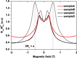
Figure 2. Normalized magnetoresistance exhibiting commensurability peaks for samples studied at 4 K. Peak of higher resistance corresponds to electron motion around one antidot. Those peaks marked by dashed line for sample D. Antidot lattice period a can be calculated from peak position in magnetic field as a = 2RC, where RC is the cyclotron radius. Commensurability peaks of lower resistance represent electron motion around 3 antidots.
Download figure:
Standard image High-resolution imageThe antidot lattice periods calculated from the major commensurability peak position in the magnetic field are given in table 1. Comparison of the calculated period with the period etched by plasma and measured by AFM provides interesting indications on effective electron motion in the antidot lattice. For all the samples, the period calculated is found to be larger than the one patterned. However, the cyclotron radius calculations indicate that electrons encircle one antidot when r < RC < a. Electrons prefer this larger cyclotron orbit when moving around semicircular antidots. The well-known formula 2RC = a is applicable to the main commensurability peak, for which the cyclotron orbit encircles one unique antidot.
The carrier density is the only parameter of the material taken into account in this calculation. However, it is evident that the cyclotron radius corresponding to a motion around one antidot depends on the antidot geometry (circular, semicircular, triangular, etc), its radius r, and the free space between adjacent antidots represented by the ratio a/r. The cyclotron radius also depends on the mobility and carrier density of the material studied. Nevertheless, to validate this hypothesis, a complete and independent study of the commensurability peaks for different antidot geometry and parameters (period, radius, and depth) should be carried out for different materials of different mobility and carrier density.
It is to be noted that the 2DEG carrier density of the Si/SiGe heterostructure is high compared with that of other most-studied materials. In addition, the low 2DEG mobility and smaller spatial separation between the antidots due to the small lattice period pose many challenges. It is probably the combination of all these characteristics that gives rise to a difference between the value of 2RC and the antidot lattice period.
The electron mobility calculated in the antidot lattice part is reported in table 1. The mobility is larger than 25 000 cm2/V.s for samples A and B but lower than 20 000 cm2/V.s for samples C and D. The lower mobilities measured for those samples were expected. Indeed, the antidot lattice etching of sample C was made deeper than the 2DEG layer, which introduced more defects into the 2DEG layer. The antidot lattice period and radius of sample D were decreased two times in comparison with those of sample B; see table 1. As a consequence, local electron depletion is increased, leading to increased interaction between electrons and the asymmetric potential induced by the asymmetrical antidots.
5. Photovoltage amplitude study for different microwave polarization
To characterize the system reaction under microwave excitation, photovoltage measurements were performed on each antidot lattice segment by using Hall probes (figure 1(c)) for configuration of the two MW linear polarizations with respect to the antidot lattice orientation. The MW polarization was chosen to be either parallel or perpendicular to the semicircular antidot lattice orientation, which corresponds to a 0 or 90 degree angle of incidence (±10°), respectively. The photovoltage response obtained for two different microwave polarizations is represented in figure 3 for sample C.
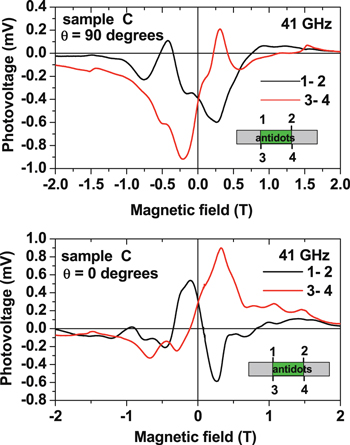
Figure 3. Ratchet photovoltage of sample C as function of magnetic field measured at 4 K. Measurements made for parallel and perpendicular microwave polarization. Microwave radiation attenuated at −10 dB.
Download figure:
Standard image High-resolution imageWithout the magnetic field, the same photovoltage value is obtained on both antidot lattice sides as expected theoretically in the case of a quasi-symmetric ratchet current flow distribution through the lattice [21]. Applying a negative magnetic field results in photovoltage that is more intense on one antidot lattice side, leading to a maximum photovoltage in a negative magnetic field for the probe pair 3–4. For a positive magnetic field, the electron antidot scattering takes place predominantly on the other antidot lattice edge, which suggests that the photovoltage response is predominant in a positive magnetic field for the probe pair 1–2. Those observations were found to be in good agreement with the theoretical investigations [21] without taking into account the e–e interaction.
When the MW polarization is rotated from 90 to 0 degrees, the ratchet flow direction is reversed, which induces a photovoltage polarity change from negative to positive as expected theoretically [7–9]. Similarly, the maximum photovoltage previously observed in a negative magnetic field is observed in a positive magnetic field and vice versa.
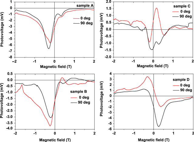
Figure 4 shows the photovoltage of different samples as a function of the magnetic field for parallel and perpendicular MW polarization. Sample B, which has the same antidot lattice period and radius as sample C, shows no photovoltage polarity change when the MW polarization orientation is changed for the magnetic field range considered. Moreover, the photovoltage maximum is always found in a negative magnetic field, which shows that changing the MW polarization angle does not affect the photovoltage intensity. This is explained by the strong e–e interaction in the Si/SiGe heterostructure, which suppresses the ratchet current flow reversibility [14, 21]. Because the e–e interaction strength is related to the carrier density equal to 6.6 × 1011 cm−2 for all the samples studied, the change in photovoltage polarity with the microwave polarization orientation observed in figure 4 for sample C is unexpected.
Figure 4. Ratchet photovoltage of samples A, B, C, and D as function of magnetic field measured at 4 K. Measurements made for parallel and perpendicular microwave polarization. Maximum microwave power used.
Download figure:
Standard image High-resolution image
To investigate this effect in more detail, we studied four samples based on Si/SiGe heterostructures with different lattice characteristics. Table 1 provides details for the antidot lattice parameters and the electronic properties of the different samples. The photovoltage polarity does not change with the MW polarization orientation for samples A and B in the magnetic field range studied. We note that the same photovoltage response to MW polarization is found for a sample having the same antidot parameters as sample A, which has a hexagonal lattice arrangement. This is not surprising because the difference between linear and hexagonal arrangements is not significant.
Sample C has the same effective antidot lattice period as sample A, but the etching depth is increased up to 72–76 nm, which means that a semicircular hole lattice is created in the 2DEG layer. In this case, an effect of the MW polarization orientation on the photovoltage polarity is observable. This is correlated with a magnetic field polarity change. The photovoltage polarity change with the microwave polarization orientation change is clearly noticeable on this sample and can be related to the fact that the 2DEG layer is composed of a real hole lattice instead of an electron depletion induced by the antidot lattice. The polarity change also implies that the amplitude of photovoltage is smaller when electron mobility is lower.
Sample D has an antidot density increased twofold compared with that of sample B. The microwave polarization effect is well observed. When rotating the MW polarization angle, the photovoltage polarity and the magnetic field polarity are reversed. The change in the polarity of photovoltage is observed in the range of the magnetic field studied.
In brief, experimental observations are as follows:
- -photovoltage polarity independence with microwave polarization for samples A and B;
- -photovoltage polarity dependence with microwave polarization for samples C and D.
The results obtained for samples A and B are explained by the strong e–e interaction, which suppresses the dependence of the photovoltage on the microwave polarization [21] otherwise observed in weakly interacting 2DEG [15]. The strong e–e interaction counteracts the action of the pointing vector orientation of the electrical field on electron motion. The e–e interaction depends on the carrier density, revealing that its strength is equal for all samples.
We argue that the modulation of the 2DEG potential by a high antidot density or the presence of a hole lattice in the 2DEG plane counteract the effect of the e–e interaction in comparison with the electron interaction with the asymmetrical potential induced by the antidots. As a consequence, the effect of the orientation of the microwave polarization on the photovoltage polarity, which is one of the bases of the ratchet-effect phenomenon, is observable even if the e–e interaction is strong. The increase of the antidot density as well as of the antidot depth etching diminish the free space between adjacent antidots in the 2DEG plane. Consequently, the electron interaction with the asymmetrical potential increases, favoring the ratchet effect and its dependence on microwave polarization.
6. Conclusions
We observed that in samples A and B, e–e interaction dominates, thereby preventing the reversal of the polarity of induced photovoltage upon changing the angle of MW polarization. Our photovoltage study clearly indicates that the antidot density and the antidot etching depth are two important parameters that significantly affect the polarity of induced photovoltage. Competition between the e–e interaction and the electron interaction with the asymmetrical antidot is observed. The deeply etched antidot sample and the sample with large antidot density showed a reversal of photovoltage polarity upon changing the MW polarization due to stronger electron depletion in the antidot lattice. We conclude that for enhancing the performance of ratchet-based devices at higher temperature, antidot lattices with higher antidot density and/or larger etching depth must be created.
Acknowledgments
We thank A D Chepelianskii, D L Shepelyansky, L Ermann, H Aubert, A Takacs, and D Medhat for fruitful discussions. The authors are very grateful to J M Hartmann from the CEA–LETI for the Si/SiGe wafer growth (PLATO-PROJECT 2002). We also thank J Florentin for technical support. This work was funded by the ANR/PNANO projects NANOTERRA and NADIA and the PUF project (France–USA), which provided financial support for E S Kannan, I Bisotto, and Y Krupko.