

Abstract
This study details the production and analysis of undoped zinc oxide (uZnO) and boron (B) doped zinc oxide nanostructured thin films, with a specific focus on assessing the influence of varying B doping concentrations on humidity sensing performance. The synthesis of undoped ZnO and B doped ZnO nanoparticles was carried out using sol–gel method. B doping concentrations within the ZnO lattice were adjusted to 1, 3, 4, 5, and 10 mol%. Subsequently, nanostructured thin films were obtained through the spin coating technique on glass substrates. X-ray diffraction analysis revealed a hexagonal wurtzite structure for all nanostructured thin films. Notably, a change in preferential orientation from the (002) plane to the (100) plane occurred when B doping concentration exceeded 5 mol%. Scanning electron microscopy showcased nano-sized grains and capillary nanopores on the surface of each thin film. Energy dispersive X-ray spectra confirmed the presence of zinc, oxygen, and boron elements in the nanostructured thin films. Humidity sensing performance was assessed through electrical resistance measurements in the range of 45%–90% relative humidity at room temperature. All fabricated sensors exhibited sensitivity to humidity. Remarkably, the sensor with a 5 mol% B doping concentration demonstrated the highest humidity sensitivity (438.44 times) and the fastest response (2.0 s) and recovery times (14.2 s). The study concluded that the optimal B doping concentration for designing a highly efficient humidity sensor was determined to be 5 mol%. Overall, the study underscores the potential of B doped ZnO nanostructures for humidity sensor applications, given their exceptional sensor performance.

Original content from this work may be used under the terms of the Creative Commons Attribution 4.0 licence. Any further distribution of this work must maintain attribution to the author(s) and the title of the work, journal citation and DOI.
1. Introduction
The role of humidity in the decay of plants, the formation of mold, the oxidation of metal materials and the negative effects on different production processes and personal comfort is quite remarkable. In addition, humidity is an important factor in the proliferation of microorganisms that carry the risk of allergies and in people with chronic diseases such as heart, asthma and diabetes [1]. These adverse events require constant detection, measurement, monitoring and control of humidity [2, 3]. This situation clearly demonstrates the need for a good humidity sensor [4, 5]. For a humidity sensor to be considered good, it depends on its ability to combine qualities such as high selectivity and sensitivity, low hysteresis, excellent repeatability, long-term stability, fast response and recovery times, easy production and low cost [6, 7]. However, it has not been possible so far to produce an ideal humidity sensor that combines all these qualities. The working mechanisms of humidity sensors are generally related to electrical changes such as capacitance (capacitive humidity sensor) and resistance (resistive humidity sensor) [8]. The disadvantage of capacitive humidity sensors is the limited distance between the sensor and the signal circuit. On the other hand, resistive humidity sensors are more advantageous due to the large distance between the sensor and the signal circuit, better sensitivity and good linearity, small size and low-cost production [9]. The correct selection of the sensing material is a parameter that plays as important a role as the preparation process and morphology in the characterization and performance of a humidity sensor, perhaps even more so [10]. In humidity sensor studies, ceramics, organic polymers, metal oxides and their nanocomposites are frequently tested as humidity sensing materials [8, 11–15].
In today's studies, metal oxide thin film nanostructures, which have superior qualities than bulk structures, have become more frequently preferred as humidity sensing materials [12]. The superior qualities of these nanostructures arise from their simple and low-cost production, smaller sizes, higher surface-to-volume ratios, higher surface charge transfer capabilities, better sensitivity, and better physical, chemical and thermal stability. Among these, the high surface-to-volume ratio quality makes nanostructures preferable for humidity sensor applications, as they can provide more surface active sites for the adsorption of water molecules, facilitate the water adsorption process, and increase the adsorption ability [16–19]. Based on these, many researchers have intensively used metal oxide semiconductor nanostructures in humidity sensor studies, and they have frequently benefited from zinc oxide (ZnO) nanostructures in these studies [10, 17–21].
ZnO has a wide direct band gap (∼3.37 eV) and large exciton binding energy (60 meV) at room temperature (RT). It is also non-toxic, sensitive to humidity and has high chemical stability. These characteristic features of ZnO are the main reason why it is frequently preferred by researchers [22–25]. Many different methods can be used for the production of ZnO nanostructures, such as molecular beam epitaxy, metal organic chemical vapor deposition, chemical vapor deposition, physical vapor deposition, vapor-liquid–solid reaction, pulsed laser deposition, sputtering, spray pyrolysis and sol–gel processing [26–33]. Among these methods, the sol–gel method has higher popularity and industrial application than other existing methods due to its many advantageous aspects [34]. The sol gel method enables the production of high-quality nanoparticles of the same size on an industrial scale. Moreover, the production of two or more types of nanoparticles can be achieved in one step. Highly homogeneous composites of very high purity (99.99% purity) can be made. In addition, ease of application, low production cost and production at low temperatures are other advantages of the sol gel method.
The use of different dopant elements and/or different dopant concentrations is one of the effective ways to change the structural, electrical and chemical character of ZnO [35]. In this way, it is also possible to eliminate or at least improve situations that may affect the humidity sensing performance such as long response and recovery times, low sensitivity and high hysteresis in the humidity sensors to be produced [9, 35–37]. The studies in the literature show that elements with very different properties such as aluminum (Al), indium (In), fluorine (F), magnesium (Mg) and strontium (Sr) are used as doping elements to increase the humidity sensing performance in humidity sensor applications based on ZnO [38–41]. On the other hand, boron (B), one of the III group elements of the periodic table, is a noteworthy element. Because, if ZnO is doped with B, the electrons that will be released when the B atom replaces the Zn atom and bonds with oxygen can increase the electrical conductivity of ZnO [42]. This can be seen as a sign that doping ZnO with B to increase its humidity sensing performance will give a positive result.
In our comprehensive literature search, we could not find any studies examining the humidity sensing performance and characteristics of B doped ZnO nanostructures. To understand the role of B in enhancing humidity sensing performance, we expanded our literature search to include the effect of B in compounds other than ZnO. However, we could only find a limited number of publications on this subject [43, 44]. In a notable contribution, Lv et al detailed the effects of B doping into TiO2, revealing the formation of oxygen vacancies and an increase in Ti3+ concentration [43]. This phenomenon led to a significant increase in humidity sensitivity. This finding served as the primary impetus for us to undertake our current study towards pioneering the investigation of the humidity sensing performance of B doped ZnO nanostructured thin films. Therefore, we thought that our study would be important in terms of filling this critical gap in the scientific literature. In this context, the main purpose of our study is to produce undoped ZnO (uZnO) and B doped ZnO (BZO) nanostructured thin films at different concentrations, and to examine the effect of B doping concentration on the humidity sensing performance of these nanostructured thin films. The originality of our study is that it will be the first study to examine the humidity sensing performance of B doped ZnO nanostructured thin films. Our study includes a holistic analysis of humidity-dependent resistance changes, sensitivity, stability, hysteresis, response and recovery times, reproducibility of measurements, and the effect of B doping concentration on humidity sensing performance. In addition, our study emphasizes the economical and simple production method used in the production of B-doped ZnO nanostructured thin films. In conclusion, our findings conclude with an assessment of the feasibility of B doped ZnO nanostructured thin films produced with cost-effectiveness and simplicity in contributing to advances in humidity sensing technologies.
2. Experimental procedures
2.1. Synthesis of nanoparticles
The synthesis of nanoparticles was carried out by the sol–gel method. Zinc acetate dihydrate (Zn(CH3COO)2·2H2O, 99.999% purity; Merck, Germany), boric acid (H3BO3, > 99.5% purity; Sigma-Aldrich, Germany), 2-methoxyethanol (CH3OCH2CH2OH, ≥ 99.3% purity; Sigma-Aldrich, Germany) and monoethanolamine (MEA; NH2CH2CH2OH, ≥ 99.5% purity); Merck, Germany) chemicals were used in the synthesis process. These chemicals functioned as zinc source, boron source, solvent and stabilizer, respectively. The molar ratios were set as 1:1 for Zn(CH3COO)2·2H2O:NH2CH2CH2OH and 0.4 M for the entire mixture solution. The mixture solutions were mixed on a magnetic stirrer with heater at 400 rpm at 80 °C for 90 min. The concentration of B doped into ZnO was varied between 1–10 mol% (1, 3, 4, 5 and 10 mol%). The amounts of precursors and reagents used for the synthesis of uZnO and BZO nanoparticles are represented in table 1 [45].
Table 1. The amounts of precursors and reagents used for the synthesis of uZnO and BZO nanoparticles.
| The amount of B doping in ZnO (mol%) | Zinc acetate dihydrate Zn(CH3COO)2·2H2O (gr) | Boric acid H3BO3 (mg) | Monoethanolamine NH2CH2CH2OH (ml) | 2-methoxyethanol CH3OCH2CH2OH (ml) |
|---|---|---|---|---|
| 0 | 4.390 | --- | 1.1 | 50 |
| 1 | 4.346 | 0.012 | 1.1 | 50 |
| 3 | 4.258 | 0.037 | 1.1 | 50 |
| 4 | 4.214 | 0.049 | 1.1 | 50 |
| 5 | 4.170 | 0.061 | 1.1 | 50 |
| 10 | 3.951 | 0.123 | 1.0 | 50 |
Solutions containing undoped ZnO and B doped ZnO nanoparticles at different concentrations were clear and homogeneous and were kept at RT for 1 day after synthesis. The flow diagram of the synthesis process is given in figure 1.

Figure 1. Flow diagram of nanoparticle synthesis and thin film preparation by sol gel method.
Download figure:
Standard image High-resolution image2.2. Preparation of nanostructured thin films
In this study, soda lime glasses were used as substrates. uZnO and BZO nanostructured thin films and humidity sensors were created on these substrates. The glass substrates were first cleaned with detergent and then with ethanol and acetone in an ultrasonic cleaner at 60 °C for 5 min each, respectively. Thus, the substrates are cleaned of unwanted dust, oil and organic or inorganic contaminants. The cleaned substrates were rinsed with deionized water and dried with dry air.
uZnO and BZO nanostructured thin films were obtained by sol–gel spin coating technique. The spin coating technique provides many advantages in coating processes [46]. Its main advantage is the absence of combined process variables. Because the presence of multiple combined process variables present in many alternative coating techniques can complicate coating control. On the other hand, the film thickness can be adjusted by changing the rotation speed and/or duration or by changing the viscosity of the coating material. Moreover, it is a low-cost and fast coating process. Another advantage of spin coating is that the film becomes increasingly uniform as it thins, thus a homogeneous and uniform coating can be obtained. During the use of this technique, first, the cleaned and dried substrates were placed in the spin coating device one by one, and then each prepared solution was dropped separately onto the glass substrates. The solutions were shaken well each time before use. The spin coating process of the substrates was carried out at 2500 rpm for 20 s and the process was repeated 6 times. During the coating process, each pre-coated film was pre-heated at 300 °C for 2 min after each layer of coating to get rid of unwanted solvents and organic precipitates. After the 6-layer coating was completed, all of the uZnO and BZO nanostructured thin films were placed in a box furnace and annealed at 500 °C for 1 h (5 °C min−1) in an ambient atmosphere [47, 48]. BZO nanostructured thin films are coded as BZO1, BZO3, BZO4, BZO5, and BZO10 for 1, 3, 4, 5, and 10 mol% B doping, respectively). The preparation stage of nanostructured thin films is shown schematically in figure 1.
2.3. Structural, morphological and elemental analyzes
After annealing, uZnO and BZO nanostructured thin films were divided into 4 equal parts of 13 × 13 mm each. One part was used for x-ray diffraction (XRD) analyses, one part was used for scanning electron microscopy (SEM) and energy dispersive x-ray spectroscopy (EDS) analyses, one part was used for electrical conductivity measurements, and another part was used for humidity measurements. XRD, SEM and EDS were used to reveal the structural, morphological and elemental characteristics of the prepared nanostructured thin films, respectively. XRD analyzes were performed with Cu Kα1 radiation (1.54 Å) in the 2θ range of 20°–80° in 1°/min steps for a full scan. Analyzes were carried out with the Bruker D8 Discover X-ray diffractometer. For SEM and EDS, FEI Versa 3D (FEG) model high-resolution scanning electron microscope (HR-SEM) with energy dispersive x-ray spectrometer (Thermo Fisher Scientific, USA) was used.
2.4. Electrical conductivity and humidity sensing measurements
Before electrical conductivity and humidity sensing measurements, electrical contacts were created on pieces cut in 13 × 13 mm dimensions for these measurements. For this, first, the nanoparticle-coated front surfaces of these parts were selectively masked (Note: for electrical measurements, masking was done in accordance with the two probe measurements and a similar procedure was followed) and these parts were placed in the thermal evaporator. Then, approximately 150 nm thick Al metal was deposited on the masked front surfaces of uZnO and BZO nanostructured thin films. Al deposition process was carried out under a pressure of approximately 10−6 Torr. Afterwards, two copper wires were connected to the Al deposited areas using conductive silver paste (EPO-TEK H20S, Epoxy Technology, USA). The conductive silver paste used to make contacts has excellent electrical conductivity, low resistance and good adhesion, and is resistant to thermal and mechanical shock. By providing electrical contacts, the samples were prepared for electrical conductivity, and humidity sensors were fabricated. The distance between contacts is 8 mm. The fabricated humidity sensors are shown with their real photographs in figure 2(a) and schematically in figure 2(b). Additionally, to compare the size of the fabricated sample, a 10 cent coin with a diameter of 19.75 mm and the sensors are shown in the same photograph in figure 2(a).

Figure 2. a) The real photos and b) schematic image of fabricated humidity sensors.
Download figure:
Standard image High-resolution imageEssentially, the measurement of relative humidity (RH) sensing is determined by measuring the change in surface conductivity. In this regard, the electrical conductivity of the produced nanostructured thin films was measured using the two-probe method [38, 39]. This method is frequently applied to measure the resistivity of very high resistivity samples such as thin films/polymer layers [49]. The measurement is based on applying electric current to the ends of two probes a few centimeters away from each other and measuring the potential difference between these two probes. The same method was preferred for electrical measurements in order to be similar to RH sensing measurements. Keithley 2400 SourceMeter (Keithly Instrument/Tektronix, USA) was used for these measurements.
A sealed humidity test chamber was utilized for humidity sensing measurements. The RH in the humidity test chamber was provided by atomized water (wet air) produced by a desktop humidifier. The processes of introducing the produced wet air into the humidity test chamber, controlling the RH percentage, and removing the wet air from the chamber were carried out with a computer-controlled Arduino-based automatic feedback controller [50]. In this way, possible fluctuations/variations of the humidifier used were minimized and measurements were made in a more controlled manner.
The RH range of the measurements was set to 45%–90%, and all measurements were made at RT under a constant current of 1 μA. The RH sensing characteristics of the fabricated humidity sensors were determined by measuring the dc electrical resistance changes of these sensors at different RH levels [38, 39]. In the measurements, Keithley 2400 SourceMeter was used as a constant current source and measuring device. Calibration of the humidity test chamber was carried out with a computer-controlled Arduino DHT22 commercial digital RH and temperature sensor (Adafruit, USA). This sensor served as the humidity indicator, controlling the different atmospheres in the humidity test chamber. All data were collected via computer, and the experimental setup used is schematically shown in figure 3.

Figure 3. Schematic representation of the experimental setup used in RH sensing measurements.
Download figure:
Standard image High-resolution image3. Result and discussion
3.1. Structural analysis
Figure 4 discloses the XRD results of the produced uZnO and BZO nanostructured thin films. Determination of crystallographic orientations was done using PDF Card No 80–0075. Figure 4 indicates that the diffraction peaks of all nanostructured thin films are in accordance with the standard diffraction peaks of the hexagonal wurtzite ZnO structure in the examination made according to the PDF card [35, 51]. Based on this, it is obvious that there is no change in the crystal structure when ZnO is doped with B, so all of the nanostructured thin films maintain the hexagonal wurtzite structure. Additionally, there is no secondary phase or impurity phase resulting from B doping in figure 4.

Figure 4. XRD spectra of the produced uZnO and BZO nanostructured thin films.
Download figure:
Standard image High-resolution imageBesides these, figure 4 indicates that B doping has an effect on the intensity and location of the diffraction peaks as well as on the preferential orientation. It can be seen in figure 4 that the sharpest diffraction peak in the XRD spectrum of uZnO is the (002) peak. This peak also indicates that the preferential orientation of the uZnO nanostructured thin film is in this direction [52–55]. However, the sharpest peak in the XRD spectra of BZO5 and BZO10 nanostructured thin films is the (100) peak. That is, the preferential orientation changed from the (002) plane to the (100) plane at high B doping concentrations. The material studied and the thermodynamics of the deposition conditions are effective parameters for the formation and direction of preferential growth [56]. The presence of the Van der Waals force between the substrate and the film highlights the effect of surface energy on the growth mode. Accordingly, the plane with the minimum interface energy determines the preferential orientation [56, 57]. Therefore, the change in preferential orientation observed in this study can be attributed to the fact that the (100) plane has a smaller surface energy than the (002) plane above a certain B dopant concentration (5 mol% for this study) when the ZnO lattice is doped with B [57–59].
On the other hand, figure 4 reveals that the intensities of (102), (101), (103) and (112) diffraction peaks slowly weaken with the increase of B doping concentration and almost disappear for 10 mol% B doping concentration. The intensity of the (101) diffraction peak first decreased for 1, 3 and 4 mol% B doping, increased slightly for 5 mol% B doping, and decreased significantly for 10 mol% B doping. The intensity of the (002) diffraction peak slowly decreased up to 3 mol% B doping concentration, and started to intensify again, albeit slightly, for doping concentrations greater than 4 mol% B doping. The intensity of the (100) diffraction peak increased with the increase of B doping concentration, and there was a very sharp increase in intensity for 10 mol% B doping concentration. In the relationship between peak intensity and crystallinity quality, it is a generally known concept that increasing the peak intensity emphasizes the increase in crystallinity quality, and decreasing the peak intensity emphasizes the decrease in crystallinity quality [60–62]. Accordingly, when B is doped into ZnO, it can be said that low B doping concentrations (1 and 3 mol%) deteriorate the crystallinity quality of nanostructured thin films, while B doping concentrations greater than 4 mol% increase the crystallinity quality and BZO10 is the nanostructured thin film with the best crystallinity quality. It is possible to explain the reason for the deterioration in crystallinity quality as the stress resulting from the size difference between Zn (0.74 Å) and B (0.23 Å) ions and the separation of B at the grain boundaries [62, 63]. The mechanism responsible for the increase in crystallinity quality may be that B atoms contribute to the reduction of defects related to oxygen (O) vacancies and interstitial sites initially occupied by Zn [53, 64].
Moreover, according to the XRD spectrum in figure 4, the position of the (100), (002) and (101) main diffraction peaks of the uZnO nanostructured thin film correspond to 31.727°, 34.4° and 36.211°, respectively. Whereas, in the XRD spectrum of BZO10, these main peaks correspond to 31.613°, 34.22° and 36.036°, respectively. A similar trend for the diffraction peaks is also present in other films with different B doping concentrations. That is, when B is doped into the ZnO lattice, the diffraction peaks shift towards smaller angles. These changes in the positions of the peaks may be related to the strain caused by point defects that may occur due to the ionic radius of B (0.23 Å) being smaller than the ionic radius of Zn (0.74 Å) [65–67].
The calculation of the structural parameters of the produced nanostructures was made using XRD data, the Debye–Scherrer formula given in equation (1) and the dislocation formula given in equation (2), and the results obtained are given in table 2 [68, 69].


where D, K, λ, β and θ represent the average crystallite size, Scherrer constant (general value was used for this study; 0.94), the wavelength of the X-ray used, the full width at half maximum of the XRD diffraction peak (FWHM) and the Bragg diffraction angle, while δ represents the dislocation density.
Table 2. Structural parameters calculated for uZnO and BZO nanostructured thin films.
| Sample name | FWHM (°) | D (nm) | δ (1/m2 × 1015) | ε × 10–3 |
|---|---|---|---|---|
| uZnO | 0.311 | 28 | 1.28 | 1.37 |
| BZO1 | 0.547 | 15 | 4.44 | 2.59 |
| BZO3 | 0.606 | 13 | 5.92 | 2.32 |
| BZO4 | 0.569 | 14 | 5.10 | 2.37 |
| BZO5 | 0.533 | 15 | 4.44 | 2.68 |
| BZO10 | 0.453 | 18 | 3.09 | 5.06 |
In order to minimize the errors in FWHM measurement and calculation of the average crystallite size, calculations were made by taking into account the strongest diffraction peak in the XRD spectrum [70]. Table 2 reveals that the structural parameters are affected by the B doping concentration.
When B was added to ZnO, FWHM increased up to 3 mol% B doping (1 and 3 mol%), and then FWHM started to decrease with the increase of B doping amount (for > 4 mol% B). The change in FWHM also affects the crystallite size according to equation (1). That is, the amount of B doping concentration also causes a change in the crystallite size of the nanostructures. According to table 2, the crystallite size decreases for 1 mol% B doping, and then as the B doping concentration increases (for > 3 mol% B), the average crystallite size increases. The main factors that determine the value of crystallite size are mainly the radius of substituted ions, lattice stress and dislocation density [71]. The stress caused by the difference in the ion radii of Zn and B and the dislocations caused by B ions occupying the interstitial regions within the ZnO crystal lattice can explain the decrease in crystallite size [67, 72]. The increase in crystallite size can also be expressed as the Zener pinnig effect [67, 72].
Another result seen in table 2 is that the dislocation density also varies depending on the B doping concentration. The dislocation density increased until 3 mol% B doping into the ZnO lattice (for 1 and 3 mol%), and then started to decrease with the increase of the B doping concentration (for > 4 mol%). Dislocation density refers to defects in the crystal structure [70]. Therefore, the mechanism responsible for the increase in dislocation density in the produced nanostructured thin films when B is doped into the ZnO lattice may be the increase in point defects resulting from the difference in the ion radii of Zn and B [69, 73].
On the other hand, while the XRD peaks of bulk materials are generally represented by a delta function, this is not the case for nanocrystals. The energy density (u) of a real nanocrystal is not isotropic. In this case, the ratio between stress and strain is non-linear [74, 75]. Therefore, it is more appropriate to use the Williamson–Hall (W-H) method to determine strain [76–78]. Considering the energy density, the relationship between the energy density and the uniform anisotropic lattice strain in each crystallographic orientation is as in equation (3) according to Hooke's law [79].

where ε is the strain and Yhkl is the Young modulus. In this case, the modified W-H equation is expressed as follows [78].

where βhkl is the width of the half-maximum intensity of instrumental corrected broadening. In this study, W-H plots of 4sinθ(2u/Yhkl )1/2 (on the x-axis) versus βhkl cosθ (on the y-axis) of each nanostructured thin film were drawn using equation (4) [79]. Energy density was determined from the slope of the linear fit made according to the data of these plots. W-H plots drawn to determine energy density are not presented in this manuscript, but the obtained values are given. Equation (3) and Yhk1 values of the hexagonal structure were used to calculate the lattice strains [78]. Approximate values determined by taking into account the margins of error in experimental measurements and calculations are given in table 2. According to table 2, the lattice strain tends to increase with the increase of B concentration. Lattice strain refers to a measure of the distribution of lattice constants resulting from crystal defects [78]. Lattice dislocation, which occurs as a result of the lattice atoms being in different places relative to the reference lattice positions, is one of the crystal defects. Accordingly, the effect of excessive volume of grain boundaries caused by dislocations may explain the increase in lattice strain [78].
Briefly, the above expressions include the possible effects of B doping on the structural characterization of ZnO nanostructure. These expressions emphasize the critical role of surface energy for preferential orientation and the possible effects of size differences between ions and defects in the structure on the observed changes in crystallinity quality, peak density and position, crystallite size, lattice stress, dislocation density and lattice strain. Understanding the complex effects of B doping on the structural characterization of ZnO nanostructures may not only help tailor their structural properties to specific applications, but may also provide implications for advancing semiconductor technology through improved material performance and functionality.
3.2. Morphological analysis
Figure 5 represents the SEM images of uZnO and BZO nanostructured thin films. Figures 5(a)–(f) emphasizes that all films have nano-sized grains and a capillary nanoporous structure, but also shows that the nano-sized grains are almost homogeneously and uniformly distributed on the surface. Nanostructured thin films containing nano-sized capillary pores/cracks and having a large surface/volume ratio generally facilitate the water adsorption process and increase the adsorption ability [7]. Overall, the findings suggest that the morphological properties of the nanostructured thin films produced in this study have significant potential for improving humidity sensor technologies and offer prospects for increased sensitivity and efficiency in real-world applications.

Figure 5. SEM images of the surfaces of (a) uZnO, (b) BZO1, (c) BZO3, (d) BZO4, (e) BZO5 and (f) BZO10 nanostructured thin films and (g) SEM image of the cross section of the BZO1 nanostructured thin film.
Download figure:
Standard image High-resolution imageAdditionally, the SEM images in figures 5(a)–(f) were carefully examined to determine the grain sizes in each nanostructure. By taking into account the randomly distributed data on the surface images of uZnO and BZO nanostructured thin films in figures 5(a)–(f), histograms of the variation in grain size along with Gaussian fitting for each film are provided and these are shown in figures 6(a)–(f) [80].

Figure 6. Histograms of grain size variations with Gaussian fit of uZnO and BZO nanostructured thin films.
Download figure:
Standard image High-resolution imageAccordingly, the average grain size of uZnO, BZO1, BZO3, BZO4, BZO5 and BZO10 nanostructures in figures 6(a)–(f) is 23.5 nm, 18.6 nm, 14.0 nm, 15.7 nm, 19.2 nm and 21.2 nm, respectively. Grain size varies depending on B doping concentration, and while it decreases for 1 and 3 mol% B doping concentrations, it increases for doping concentrations higher than 4 mol% B doping concentration. The change in grain sizes depending on the doping concentration is consistent with XRD measurements. However, since the grains are crystal bundles arranged in the same direction, the grain sizes determined by SEM images are slightly larger than the crystallite sizes determined by XRD analysis [81].
In addition, the film thickness of each structure was determined from the cross-sectional SEM images of the structures, and the cross-sectional image of the BZO1 nanostructured thin film is given as a representative in figure 5(g). Based on data obtained from all cross-sectional SEM images, the average film thickness was assessed as 1000 nm.
3.3. Elemental analysis
The elemental contents of the produced uZnO and BZO nanostructures were clarified by EDS analysis. Elemental content analysis was carried out as regional scanning on each nanostructured thin film surface [82]. The scanning result showed the relative proportions of the elements in the scanned region. Elemental analyzes were performed for all nanostructures. The EDSs of all produced thin films is not the same, but similar. In all EDSs, all peaks belonging to the relevant elements were obtained based on regional scanning, and only the intensity of the peaks varies depending on the elemental ratio. Therefore, to avoid similar figures, BZO10 nanostructured thin film served as a representative in figure 7. Figure 7 clearly emphasizes that Zn, O and B elements, which are the main elements of the structure, exist in the BZO10 nanostructured thin film [65, 83].

Figure 7. EDS spectrum of BZO10 nanostructured thin film.
Download figure:
Standard image High-resolution imageHowever, it is also possible to see peaks in the EDS spectra that belong to the glass substrate and/or whose origin cannot be identified by the measuring device, as seen in the characteristic X-ray energies of ∼0.24–0.29 keV, ∼0.80–0.90 keV and ∼1.70–1.80 keV in figure 7. In this case, the general practice is to remove peaks that belong to the substrate and/or whose origin cannot be identified from the EDS spectra and normalize the values. For example, the peak seen at ∼0.80–0.90 keV in figure 7 was seen in the EDS spectrum of ZnO in many studies in the literature, but could not be identified and was evaluated together with the main Zn peak [84]. For this reason, peaks of elements such as silicon (Si) and calcium (Ca), which are thought to belong to the glass substrate, and unidentified peaks were removed from the EDS spectra, the values were normalized for the main elements Zn, B and O, and the results are displayed in table 3.
Table 3. Normalized weight percentages (wt%) of the main elements of uZnO and BZO nanostructured thin films.
| Sample name | Normalized weight percentage of Zn (wt%) | Normalized weight percentage of O (wt%) | Normalized weight percentage of B (wt%) |
|---|---|---|---|
| uZnO | 84.21 | 15.79 | --- |
| BZO1 | 72.54 | 16.62 | 10.84 |
| BZO3 | 64.66 | 22.78 | 12.56 |
| BZO4 | 64.69 | 21.75 | 13.56 |
| BZO5 | 64.11 | 22.04 | 13.85 |
| BZO10 | 55.47 | 20.73 | 23.80 |
Table 3 highlights that Zn, O, and B elements are present in each nanostructured thin film, and the weight percentage of B element in the scanned region increases with the increase in B doping concentration [65, 83]. Additionally, table 3 is an indication that the stoichiometric calculations for BZO nanostructured thin films are relatively accurate.
3.4. Electrical measurements
The electrical resistivities of the produced nanostructured thin films were measured and calculated by the two-probe method as approximately 4.35 Ωcm, 29.46 Ωcm, 62.64 Ωcm, 14.72 Ωcm, 103.38 Ωcm and 128.82 Ωcm for uZnO, BZO1, BZO3, BZO4, BZO5 and BZO10, respectively. Although it decreased slightly for 4 mol% B doping concentration, the resistivity of ZnO gradually increased for 1, 3, 5, and 10 mol% B doping concentration. This can be interpreted as the resistivity of nanostructured thin films generally increases (therefore their conductivity decreases) with the increase in B doping concentration. The increase in resistivity of BZO nanostructured thin films can be attributed to the fact that lattice disturbances caused by B ions doped into the ZnO lattice (which is consistent with our XRD results) increase the probability of scattering [85–87].
3.5. Humidity sensing measurements
Before starting the humidity sensing measurements, the resistance of each humidity sensor in air was measured using the Keithley 2400 SourceMeter, and the resistances of uZnO, BZO1, BZO3, BZO4, BZO5 and BZO10 were recorded as 4.89 MΩ, 640 MΩ, 5.02 GΩ, 340 MΩ, 38.1 GΩ and 69.4 GΩ, respectively. It is thought that the high resistance recorded for these sensors may be due to the electrical contacts provided on these films and/or the capillary nanoporous surface that all these sensors have, as can be seen in the SEM micrographs [88]. Figure 8 exhibits the effect of relative humidity (RH%) on the resistances of uZnO, BZO1, BZO3, BZO4, BZO5, and BZO10 humidity sensors.

Figure 8. Effect of RH% on the resistance of uZnO and BZO humidity sensors.
Download figure:
Standard image High-resolution imageIn order to minimize the margin of error in the measurements, each measurement was repeated 5 times with 1 day intervals and the experimental error average of the 5 measurements was taken. Based on this, all measurements and calculations are evaluated with a tolerance of ± 2%. Figure 8 declares that the effect of RH% on the resistance of humidity sensors is that the resistance of humidity sensors decreases as RH% increases. That is, all fabricated sensors exhibit sensitivity to humidity. In figure 8, except for the uZnO sensor, the resistance change of the other sensors is generally quite fast at 45%–55% RH, while it is relatively slow between 55%–90% RH. This is an indication that the humidity sensitivity of these sensors is quite high in the 45%–55% RH range and relatively low in the 55%–90% RH range.
The decrease in electrical resistance of fabricated humidity sensors as the RH% increases is essentially related to the shape, size and nature of the surface of these sensors, the size of the particles on the surface, and the amount of water molecules adsorbed on this surface [19, 48, 89]. The size of the particles is in the range of nanometers, allowing the surface area on which water molecules to be adsorbed to be larger [90]. Thus, a greater number of charge carriers will contribute to the conductivity as a greater number of water molecules can be adsorbed on this surface [10, 90]. According to our XRD and SEM analyses, the sensors we produced in this study have nano-sized particles and the sensor surfaces contain capillary nanopores. This structural and morphological character may help understand the reason for the decrease in resistance of our sensors as %RH increases.
The humidity sensing mechanism responsible for the change in resistance depending on RH% is a process that includes chemical adsorption (chemisorption), physical adsorption (physisorption) and capillary condensation, and the Zn2+ ions on the material surface and the morphology of the humidity-sensing metal oxide material are the critical parameters of this process [37, 75, 91, 92]. According to figure 8, the resistances of BZO humidity sensors change quite rapidly at low relative humidity. The rapid change of resistance means that water molecules are chemically adsorbed on the metal oxide surface and a chemisorbed layer of water vapor is formed on the sensor surface [93]. As a result of the interaction of water molecules with the sensor surface, free electrons are released. The interaction of water molecules with the sensor surface results in the release of free electrons and this leads to the decrease in resistance. Metal cations and hydroxyl ions of dissociated water molecules form covalent bonds and cause the emergence of mobile protons [75]. In this case, conduction occurs by the movement of these mobile protons from site to site via the Von Grotthuss mechanism (proton hopping mechanism) across the surface in this first chemically absorbed layer. The increase in relative humidity results in the physical adsorption of new water layers on top of the first chemically adsorbed layer. If the relative humidity increases further, physisorption on the film surface causes the formation of a multilayered water layer in series. In this case, the change in resistance depending on relative humidity is low due to the layers formed on the film surface [93]. Conduction in the physisorbed layer takes place with mobile protons moving freely in the liquid-water layer according to the Grotthuss mechanism [91]. At higher relative humidity levels, the number of water molecules adsorbed to the metal oxide surface will further increase. This causes the capillary pores to reach saturation, and then water vapor condenses in these pores [92]. As a result, at higher relative humidity levels, the resistance decreases significantly and saturates [93].
Figure 9 are graphs expressing how the sensitivity of the humidity sensors fabricated in this study changes depending on the RH%. According to figure 9, each of the uZnO and BZO humidity sensors is sensitive to RH%. However, the degree of humidity sensitivity of each humidity sensor differs depending on the B doping concentration they contain.

Figure 9. Humidity sensitivities of fabricated humidity sensors depending on RH%.
Download figure:
Standard image High-resolution imageIn order to perceive this difference more clearly, the humidity sensitivity ratings of all sensors according to 90% RH were calculated with equation (5) and the approximate values are given in table 4 [94].

where S, Ra and Rrh express the humidity sensitivity of the sensor, the resistance of the sensor in air and the resistance of the sensor at different RH%, respectively. In the calculations, the resistance of the sensors at 45% RH was taken into account as the Ra value [95].
Table 4. Humidity sensitivity ratings of fabricated humidity sensors according to 90% RH.
| Sample name | Sensitivity (S) (for 90% RH) |
|---|---|
| uZnO | 1.45 |
| BZO1 | 8.68 |
| BZO3 | 19.02 |
| BZO4 | 24.46 |
| BZO5 | 438.44 |
| BZO10 | 50.02 |
Figure 9 and table 4 indicate that both B doping and the amount of B doping concentration are highly effective on the humidity sensitivity of the sensors. When the humidity sensitivities were compared with uZnO, the sensitivity gradually increased up to 5 mol% B doping, the increase peaked significantly for 5 mol% B doping, and the sensitivity decreased again for 10 mol% B doping. Among the B doped ZnO humidity sensors, the sensor with the highest humidity sensitivity is BZO5, and the sensor with the lowest humidity sensitivity is BZO1. While the humidity sensitivity degree of BZO1 between low RH (45%) and high RH (90%) was calculated as 8.68 times, the humidity sensitivity degree of BZO5 between RH (45%) and high RH (90%) was calculated as 438.44 times.
Grain size and crystallinity quality stand out as factors that have a remarkable impact on the humidity sensitivity of humidity sensors [96]. High crystallinity quality and/or smaller particle size have an increasing effect on humidity sensitivity [75]. It was determined from XRD analysis that the structure with the highest crystallinity quality was BZO10. However, it can be seen in table 4 that the humidity sensitivity of this structure is much lower than BZO5. Accordingly, even if the crystallinity quality is low, if the structure has smaller grain sizes, the humidity sensitivity of that structure may be higher. Because the decrease in particle size in the structure will increase the active surface area, this may lead to an increase in the number of adsorbed water molecules, thus increasing humidity sensitivity [75, 96]. It was concluded through SEM analysis that the grain size of BZO5 is smaller than that of BZO10. In this case, in view of the above expression, the active surface area of BZO5 is likely to be larger than that of BZO10. Therefore, it would be normal for the BZO5 sensor to have the highest humidity sensitivity. On the other hand, the grain sizes of BZO1, BZO3 and BZO4 are smaller than those of BZO5, but their humidity sensitivity is much lower because their crystallinity quality is lower than BZO5. Considering the highest humidity sensitivity within the scope of this study, it was concluded that the optimum amount of B doping concentration to be doped into ZnO could be 5 mol%.
In summary, the information obtained from humidity sensing measurements points to the importance of B doping and morphological structure in increasing humidity sensor sensitivity and underlines the critical role of B doping concentration, grain size and crystallinity quality in determining the humidity sensitivity degree of sensors. These findings may pave the way for tailored B-doping strategies to optimize sensor performance to meet highly sensitive humidity sensor expectations in various fields, including environmental monitoring, industrial processes, and healthcare, thus shedding light on innovation in sensor technology.
Additionally, the sensitivities of the humidity sensors fabricated in this study were compared with other studies on this subject in the literature and the results are given in table 5. According to the comparison results, an idea was obtained as to whether the sensitivities of the fabricated sensors were good or not.
Table 5. Humidity sensitivities of fabricated humidity sensors in the literature and in this study.
| Material | Method | Sensitivity | References |
|---|---|---|---|
| ZnO thin film | The chemical bath deposition | 70.1 | [97] |
| Poly(triphenylamine) (PTPA) into poly(vinylidene fluoride)(PVDF) nanofibers (NFs) | Electrospinning | 2.9 | [98] |
| Magnesium oxide (MgO) nanoparticles | Green synthesis | 99.84 | [99] |
| Poly Vinylidene Fluoride (PVDF)/Polymethyl Methacrylate (PMMA)/ZnO hybrid nanocomposite thin films | Sol–gel | 63.43 | [100] |
| Erbium Oxide (Er2O3) nanospheres | One-step solvothermal | 403 | [101] |
| Silver (Ag)–ZnO nanocomposites | The chemical reduction | 5.25 | [102] |
| Al doped ZnO | Ultrasonic solution immersion | 77.3 | [103] |
| ZnO / Tin Oxide (SnO2) Nanostructure Film | Electrospraying | 7.46 | [104] |
| Fe doped SnO2 nanocoral (FSNC) | Hydrothermal synthesis | 68.03 | [4] |
| Iron tungstate-tungsten trioxide (FeWO4–W03) composite nanoparticles | Solid state | 3956 | [105] |
| Copper ferrite–yttrium oxide (CFYO) nanocomposite | Mechanochemical | 4895 | [106] |
| B doped ZnO | Sol–gel | 438.44 | This study |
Table 5 clearly reveals that the humidity sensitivity of the sensors fabricated in this study is much better than the structures produced in many studies in the literature. This table can be seen as a sign that B doped ZnO nanostructured thin films have humidity sensor potential and that these nanostructures can be considered for applications in this field. However, Poovaragan et al and Babu Reddy et al obtained very high sensitivity values in their studies [105, 106]. Even though these values are higher than the values obtained in this study, our study can be considered more noteworthy because we can produce our sensors easily and at low cost.
The long-term stability of the humidity sensing characteristics of the fabricated sensors was evaluated by repeating each measurement for each sensor candidate. Measurement repetitions were carried out in two stages. The first was performed in the first 5-day period immediately after the fabrication of the sensors, while the second was carried out in the 25-day period 1 month after the fabrication of the sensors. Figure 10 shows the stability over a 25-day period for the fabricated humidity sensors. The insert figure in figure 10 represents the stability over a 5-day period for each sensor. Long-term stability curves were obtained by measuring resistance values under 90% RH conditions for each measurement. When figure 10 was compared with the insert figure in figure 10, it was determined that both figures had similar characters and that there was only a slight increase in the resistance of the sensors after 1 month. Accordingly, although there are small differences between the resistance values measured in each measurement, it can be assumed that all humidity sensor candidates have adequate and good stability. The consistent stability observed as a result of evaluating long-term stability increases the potential for reliable and long-term use of these humidity sensor candidates in practical applications in real-world conditions and promises sustained effectiveness in humidity sensing tasks.

Figure 10. Long-term stability of fabricated humidity sensors.
Download figure:
Standard image High-resolution imageA sensor should have low hysteresis in relation to the stability and reliability of the sensor material [107]. In this regard, he reliability and stability of the fabricated humidity sensors were tested with hysteresis measurements. The same operations were carried out for all humidity sensors and similar graphics were obtained as a result of the operations. For this reason, only the hysteresis curve of the BZO5 sensor is given as a representative in figure 11. The curve expresses the time delay between the adsorption and desorption processes during the increase and decrease of RH%. The width of the loop formed in figure 11 gives a preliminary idea about the hysteresis error rate, and for a reliable sensor, it is desirable that the loop have a narrow structure [93].

Figure 11. Hysteresis curve between adsorption and desorption processes of BZO5 sensor.
Download figure:
Standard image High-resolution imageThe hysteresis error rates detected for each humidity sensor produced were calculated using hysteresis curves and equation (6) [108].

where γH ; hysteresis error rate, ΔHmax ; difference between the output of adsorption and desorption processes and FFS ; full scale output symbols. The hysteresis error rate of all sensors was calculated using figure 11 and equation (6). Accordingly, the hysteresis error rates of uZnO, BZO1, BZO3, BZO4, BZO5 and BZO10 sensors were found to be approximately 16.4%, 15.7%, 15.7%, 15.9%, 14.7% and 15.1%, respectively. Although the measurements for the fabricated sensors include hysteresis, it is predicted that these humidity sensors can be considered reliable because the hysteresis error rates are relatively low. However, it can be said that BZO5 may have a better performance as a humidity sensor compared to others since it has the lowest hysteresis error rate among the fabricated humidity sensors. On the other hand, the hysteresis that may exist in structures of this nature can be attributed to the residual water molecules remaining on the surface of the sensor, that is, the humidity absorbed during adsorption does not evaporate completely during desorption [109, 110]. The presence of relatively low hysteresis observed in fabricated humidity sensors indicates their potential reliability for practical applications, as it will not significantly degrade the effectiveness of the sensors. This points to positive prospects for the development of reliable humidity sensing technologies, especially with the potential for further optimization of sensor materials and design.
Since the reproducibility of the measurements can give an idea about the consistency of the humidity sensor performance, the reproducibility of the performances of all sensors produced was tested [111, 112]. Measurements of the reproducibility of the sensor performance were carried out for 9 cycles under a constant current of 1 μA. Since graphs with similar characteristics were obtained for all sensors as a result of the measurements, the curve obtained for the BZO5 sensor is presented representatively in figure 12.

Figure 12. Reproducibility of sensor performance of the BZO5 humidity sensor.
Download figure:
Standard image High-resolution imageAs seen in figure 12, the same type of character was observed in each of the 9 cycles. The observed character for 9 cycles is that the resistance increases when the RH% decreases and the resistance decreases when the RH% increases. Exhibiting a similar character in each cycle is a result of the reproducibility of sensor performance. Since this is also valid for all sensors, it is possible to say that the performances of all sensors fabricated in this study are reproducible. The consistent and reproducible performance observed across multiple cycles for all fabricated sensors suggests a high level of reliability in their functionality. This result is noteworthy as it can meet expectations in terms of reliable humidity sensing performance.
The response and recovery time of a humidity sensor is almost one of the most critical sensor characteristics. Therefore, the response and recovery times of all sensors fabricated in this study were also determined. Graphs obtained from reproducibility measurements were used to determine these times. Since calculations were made on the same type of graphs of all fabricated sensors, only the graph of the BZO5 humidity sensor is shown as a representative in figure 13 in order to avoid repetition.

Figure 13. Response and recovery time graph of BZO5 humidity sensor.
Download figure:
Standard image High-resolution image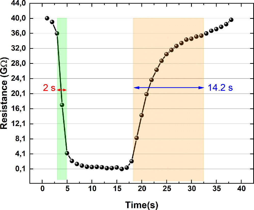
Figure 13 shows the times in the sections containing 90% of the resistance changes occurring during the adsorption and desorption processes in a single cycle in figure 12. The duration of the adsorption process (from 45% to 90% RH) was considered as the response time, while the duration of the desorption process (from 90% to 45% RH) was considered as the recovery time. A similar process was applied for all fabricated sensors (using the reproducibility graph of each sensor) and the response and recovery times obtained are given in table 6.
Table 6. Response and recovery times of fabricated humidity sensors.
| Sample name | Response time (s) | Recovery time (s) |
|---|---|---|
| uZnO | 3.6 | 19.2 |
| BZO1 | 9.7 | 27.6 |
| BZO3 | 4.6 | 16.4 |
| BZO4 | 5.2 | 20.2 |
| BZO5 | 2.0 | 14.2 |
| BZO10 | 2.8 | 15.7 |
Table 6 highlights that the response and recovery times of the sensors vary depending on the B doping concentration. Accordingly, the response and recovery times shortened up to 3 mol% B doping concentration (for 1 and 3 mol%), increased slightly for 4 mol% B doping, reached their shortest values for 5 mol% B doping, and increased again for 10 mol% B doping.
The short response and recovery times for concentrations higher than 4 mol% B doping concentration may be related to the O-containing hydrophilic functional groups that may exist in the surface layer of these sensors and/or the interlayer distance in these nanostructures being wide enough to facilitate water adsorption and desorption [44, 113]. On the other hand, the increase in times (especially recovery time) for 10 mol% B doping concentration may be due to the increase in the interfacial hydrophilicity of the BZO10 nanostructure with the increase of doping concentration and/or the slow desorption kinetics of water vapor [110, 114, 115]. According to table 6, BZO5 sensor has the shortest response and recovery times of 2.0 s and 14.2 s, respectively. The reason why the BZO sensor has the best response and recovery times can be attributed to the relatively faster adsorption and desorption of water molecules on its surface due to its texture containing nano-sized capillary pores [93]. This research on response and recovery times underscores the critical role of B doping concentration in optimizing sensor performance. Specific to this study, the results show that 5 mol% B doping concentration represents the optimal balance to achieve fast response and recovery times in humidity sensors, and expectations for efficient and fast sensing can be met.
In addition, the response and recovery times of the humidity sensors fabricated in this study were compared with the times presented in different studies in the literature and the comparison is displayed in table 7. Table 7 demonstrates that the humidity sensors we fabricated in this study have much faster response and recovery times than many fabricated humidity sensors in the literature. On the other hand, table 7 shows that much faster humidity sensors are also available. However, we think that low cost and ease of production can bring our sensors to the forefront.
Table 7. Response and recovery times obtained in the literature and in this study.
| Material | Method | Response time (s) | Recovery time (s) | References |
|---|---|---|---|---|
| TiO2/ZnO composites | Hydrothermal | 18 | 22 | [116] |
| (In+Nb) co-doped HfO2 ceramics | The solid-state reaction | 20 | 50 | [117] |
| Poly(triphenylamine) (PTPA) into poly(vinylidene fluoride)(PVDF) nanofibers | Electrospinning | 33 | 28 | [98] |
| Cerium dioxide (CeO2)/molecular sieve type 4A composite (CeO2/4A) | Simple | 9 | 80 | [118] |
| Poly Vinylidene Fluoride (PVDF)/Polymethyl Methacrylate (PMMA)/ZnO hybrid nanocomposites | Sol–gel | 26 | 12 | [100] |
| TiO2/KNbO3 nanocomposite | Two-step hydrothermal | 3 | 163 | [119] |
| Graphene oxide (GO) film | The drop-casting method | 0.28 | 0.3 | [120] |
| Er2O3 nanosphere | Solvothermal | 1 | 5.1 | [101] |
| Rubidium-doped Magnesium ferrite | The self-propagating high temperature synthesis | 20 | 30 | [121] |
| Ag-ZnO nanocomposites | The chemical reduction | 54 | 73 | [102] |
| Molybdenum disulfide (MoS2) nanosheets | Ultrasound-assisted liquid phase exfoliation | 30 | 40 | [112] |
| Copper ferrite-yttrium oxide (CFYO) nanocomposite | Mechanochemical | 9 | 23 | [106] |
| B doped ZnO | Sol–gel | 2 | 14.2 | This study |
4. Conclusions
This study delves into a comprehensive examination of the humidity sensing performances exhibited by BZO nanostructured thin films. Key parameters under scrutiny include humidity-dependent resistance changes, sensitivity, stability, hysteresis, reproducibility of measurements, as well as response and recovery times, with a particular emphasis on the influence of B doping concentration on these performances. uZnO and BZO nanostructured thin films obtained by sol–gel spin coating technique exhibit a hexagonal wurtzite structure. Notably, a change in preferential orientation from the (002) plane to the (100) plane occurred when B doping concentration exceeded 5 mol%. The surface of the films has homogeneously and uniformly distributed nano-sized grains and capillary nanopores, rendering them well-suited for humidity sensor applications. All fabricated sensors were sensitive to humidity, and BZO5 sensor containing 5 mol% B doping concentration exhibited the highest sensitivity with 438.44 times. BZO5 sensor also demonstrated the fastest response time (2.0 s) and recovery time (14.2 s) among all sensors. These findings underline the idea that the optimal B doping concentration for designing a high-performance humidity sensor within the scope of this study was determined as 5 mol%. Moreover, BZO nanostructures are emerging as reliable humidity sensors with long-term stability and reproducibility in humidity measurements. Importantly, BZO humidity sensors fabricated in this study outperform many of their counterparts in the literature with higher sensitivity and significantly faster response and recovery times. Consequently, their remarkable characteristic sensor performance positions BZO nanostructures as having significant potential for humidity sensor applications.
Acknowledgments
This study was funded by the Scientific Research Projects Coordination Unit of Istanbul University. Project numbers are FYL-2017-24168 and FDK-2021-38266.
Data availability statement
The data cannot be made publicly available upon publication because the cost of preparing, depositing and hosting the data would be prohibitive within the terms of this research project. The data that support the findings of this study are available upon reasonable request from the authors.
Conflicts of interest
The authors declare no conflict of interest.
Author contributions
Gökhan Algün: Conceptualization, formal analysis, investigation, methodology, resources, validation, visualization, writing–original draft, writing–review & editing; Marwa Alshater: Conceptualization, investigation; and Namık Akçay: Data curation, formal analysis, resources, software, visualization, writing–review & editing.