
Abstract
The compositional effect of Mo/W ratio on linear, nonlinear absorption and optical limiting behavior of the NaBi(MoxW1−xO4)2 single crystals grown by Czochralski technique was investigated. X-ray diffraction patterns of the studied crystals presented well-defined peaks associated with the tetragonal crystalline structure. The nonlinear absorption performance and optical limiting threshold were determined using an open-aperture Z-scan technique. A theoretical model including one photon absorption (OPA), two photon absorption (TPA) and free carrier absorption was used to determine the nonlinear absorption parameters. All of the results showed that defect states, which strongly affect nonlinear absorption (NA) and optical limiting behaviors, can be tuned with the Mo/W ratio, enabling NaBi(MoxW1−xO4)2 single crystals to be used in desired optoelectronic applications. Linear optical absorption analysis revealed that bandgap energy and defect states can be tuned by changing the Mo/W ratio in the crystal structure. The obtained results showed that all the studied crystals had NA behavior and the nonlinear absorption coefficient decreased with increasing Mo/W ratio. Sequential TPA is the main NA mechanism for these crystals due to the fact that the incident light energy is lower than the bandgap energies and the existence of the real intermediate state around 2.32 eV.
Export citation and abstract BibTeX RIS

Original content from this work may be used under the terms of the Creative Commons Attribution 4.0 licence. Any further distribution of this work must maintain attribution to the author(s) and the title of the work, journal citation and DOI.
1. Introduction
Double tungstates and molybdates formulated as AB(YO4)2 (A: monovalent cation; Li+, Na+ or K+, B: trivalent one; Ln3+, Y3+, or Bi3+, Y: Mo6+ or W6+) have been a significant research interest thanks to their structural and optical features [1, 2]. These compounds crystallize in two phases belonging to the monoclinic and tetragonal structures [1].The high refractive index, nonlinear optical characteristics, luminescence properties, wide transmission range and large optical bandwidths make these compounds potential candidates in laser, light emitting diode, optical amplifier, and nonlinear optical device applications [3–5]. NaBi(WO4)2 and NaBi(MoO4)2 are two members of this group and the device applications of these compounds are increasing in recent years. Device application studies indicated that NaBi(MoO4)2 and NaBi(WO4)2 may be used in light emitting diodes, scintillators, temperature sensors, gas sensing devices [6–11]. Both compounds crystallize in tetragonal structure with reported lattice parameters of a = b = 5.272 Å, c = 11.577 Å for NaBi(MoO4)2 and a = b = 5.265 Å, c = 11.429 Å for NaBi(WO4)2 [12–14]. In the crystal structure, each Mo and W element is attached to four O-atoms and thanks to these bonds, MoO4 and WO4 tetrahedron structure are formed. Random distribution of Na+ and Bi3+ atoms in the crystal structure caused these compounds to have a disordered structure. NaBi(WO4)2 and NaBi(MoO4)2 compounds can be synthesized/grown in single crystal, thin film and nano structures. Although this situation causes changes in the band energies of the compounds, the bandgap energies of NaBi(MoO4)2 and NaBi(WO4)2 are generally reported to be around 2.90 and 3.50 eV, respectively [14–17].
NaBi(MoxW1−xO4)2 compounds are formed as a result of replacing Mo element with W element. The most important advantage of obtaining such compounds is that the structural and optical properties can be adjusted depending on the composition. The tuning behavior of the optical characteristics supplies a noteworthy advantage especially in optoelectronic applications. For example, the photoluminescence study on GaS1−xSex nanobelts showed that the materials give emissions that vary with the composition in the range of 490–620 nm (2.0–2.5 eV) [18]. It is possible to design a device emitting specific light within this region by adjusting the composition. The studies on ZnxMg1−xO indicated that crystal structure and emission characteristics change depending on the composition [19]. It was reported in [19] that Mg-rich compounds may be used to design optoelectronic devices operating at deep UV range. There are limited studies on NaBi(MoxW1−xO4)2 compounds in the literature. In our recent study, the structural and optical properties of NaBi(Mo0.5W0.5O4)2 single crystal were reported [13]. The direct bandgap and Urbach energies of the crystal were reported as 3.18 and 0.17 eV, respectively [13]. A recent paper reported the microwave dielectric properties of compounds corresponding to compositions of x = 0.0, 0.5 and 1.0 [20]. The reported characteristics indicated that (Na0.5Bi0.5)(Mo1−xWx)O4 ceramics have significant potential to be utilized in low temperature co-fired ceramic area. Considering the device application effectiveness of the NaBi(MoxW1−xO4)2 compounds, the present paper aimed at investigating NA characteristics of the single crystals of compositions x = 0, 0.5 and 0.75. NA and optical limiting characteristics of these compounds were revealed for the first time with this study. For this purpose, open aperture (OA) Z-scan measurements were accomplished at 532 nm irradiation wavelength by increasing the input densities to reveal NA behavior of the NaBi(MoxW1−xO4)2 single crystals. Optical limiting characteristics were also investigated. The dependence of the revealed optical parameters on Mo/W ratio was discussed throughout the paper.
2. Experimental section
2.1. Growth of NaBi(MoxW1−xO4)2 single crystals
NaBi(MoxW1−xO4)2 single crystals for compositions of x = 0, 0.5 and 0.75 were grown by Czochralski method [13, 21]. Bi2O3, MoO3, WO3 and Na2CO3 starting compounds were used in the required ratios for each crystal. The starting compounds used in stoichiometric ratios were mixed and then pelleted. The pellets were heated at 700 °C–800 °C for 20–24 h to obtain a single phase. Throughout the growing process, 2 mm h−1 pulling rate and 15 rpm rotation rate was applied. After the end of the crystal growth process, small rectangular prism-shaped pieces were cut from the large ingot and these pieces were polished. NaBi(MoxW1−xO4)2 single crystals for x = 0, 0.5 and 0.75 were represented as crystals 1, 2 and 3 in this report.
2.2. Characterization methods
X-ray diffraction (XRD) experiments are used to analysis of structural characterization of the grown crystals. Rigaku miniflex model diffractometer emitting CuKα radiation at wavelength of 0.154049 nm from 20 to 50° with a speed of 0.02°/s was used for XRD measurements. The thicknesses of the single crystals were measured at around 0.4 cm. UV-1800 model Shimadzu UV–vis spectrophotometer was used to reveal the linear optical behavior of the NaBi(MoxW1−xO4)2 (at x = 0, 0.5 and 0.75) single crystals. OA Z-scan experiments with Q-switched Nd:YAG (Quantel Birillant) laser (10 Hz repetition rate, 4 ns pulse duration) at 532 nm excitation wavelength were carried out to determine nonlinear optical behavior of the crystals. The beam waist radius (ω0) at the focus was used as 22 μm, Rayleigh length were calculated to be 2.85 mm for 532 nm. The OA experiments were performed at 0.8, 2.7 and 4 μJ input energies and at 13.23, 44.10 and 66.16 MW cm−2 the input intensities.
3. Results and discussions
3.1. Materials characterizations
Figure 1 depicts the XRD patterns of NaBi(MoxW1−xO4)2 crystals. XRD patterns show sharp peaks at 31.30° and 64.95° for crystal 1, 34.60° and 70.00° for crystal 2, 35.20° and 70.90° for crystal 3. The presence of these peaks shows that grown compounds were successfully obtained in single crystal form. The peaks seen in the XRD patterns of crystals 1 and 2 are in good accordance with the literature's previously published peaks [13]. Considering the [20], the observed peaks are related to tetragonal crystalline structure of the studied crystals and figure 1 shows the corresponding Miller indices on the peaks. When the positions of the peaks observed for each crystal in the figure were compared, it was seen that the angle position of the peaks seen at high degrees corresponded to almost twice the angle position of the peaks seen at low degrees. This shows that the planes of the respective peaks are parallel to each other. For example, the (200) plane of the peak at 35.20° observed for crystal 3 is parallel to the (400) plane of the peak at 70.90°. This can be interpreted as the orientation of crystal surfaces in a single plane. The values of particle sizes (D) were were found to be 61.02, 29.92 and 44.43 nm for 1, 2 and 3 crystals, respectively, which were calculated using the Scherrer's equation (D = 0.94λ/β cosθ) [22]. Herein, θ is the Bragg angle, β is the FWHM and λ refers to the wavelength of the x-ray.
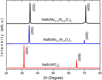
Figure 1. XRD patterns of single crystals 1, 2 and 3.
Download figure:
Standard image High-resolution image3.2. Linear absorption analysis
Figure 2(a) indicates linear absorption behavior of crystals 1, 2 and 3. The Mo/W ratios are 0, 1 and 3 for crystal 1, 2 and 3, respectively. As can be seen from this figure, the increased Mo/W ratio resulted in increased absorption with slightly shifted absorption band edge towards the longer wavelength. The energy of forbidden bandgap is obtained by the following expression [23]

where n = 1/2 and n = 2 for direct and indirect transitions taking place between valence and conduction bands, Eg is forbidden bandgap energy, α is absorption coefficient, A is a constant and hν is photon energy. Due to the direct transition of the crystals 1, 2 and 3, (αhν)2 versus hν graphs (Tauc plot) presented in figure 2(b) give the Eg values of the studied single crystals. The Eg values are found as 3.47, 3.24 and 3.13 eV for crystals 1, 2 and 3. The reported bandgap energies of the NaBi(MoO4)2 and NaBi(WO4)2 crystals are around 2.90 and 3.50 eV, respectively [14, 15]. It is clearly seen that increasing Mo/W ratio in the crystal led to decreasing bandgap energy. This also means that the Eg value of NaBi(MoxW1−xO4)2 single crystals can be adjusted for desired optoelectronic applications by varying the Mo/W ratio. The tuning characteristics of the bandgap energy of NaBi(MoxW1-xO4)2 compounds provide a remarkable advantage for optoelectronic applications.

Figure 2. (a) Linear absorption spectra and (b) (αhν)2 versus hν graphs (Tauc plots) of crystals 1, 2 and 3.
Download figure:
Standard image High-resolution imageNonlinear optical behavior and nonlinear absorption mechanisms are strongly associated with the defects in the structure as well as bandgap energy of the materials [24–28]. The tail width of absorption band edge, known as the Urbach tail, is used to reveal the defects just below the conduction band using the following expression [29]

where α0 is a constant, EU is the Urbach energy and α is the linear absorption coefficient. The inverse slope of the linear region of the lnα with respect to hν graphs presented in figure 3 provides the EU values of the samples. The values of EU are calculated as 0.37, 0.17 and 0.15 eV for crystals 1, 2 and 3, respectively. Decreasing EU value with increase of the Mo/W ratio is the evidence of the decreasing defects in the structure [30, 31].
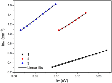
Figure 3. lnα versus hν plot of crystals 1, 2 and 3.
Download figure:
Standard image High-resolution image3.3. Nonlinear absorption and optical limiting analysis
OA Z-scan measurements are conducted at 532 nm irradiation wavelength under several input densities to bring out the NA properties of 1, 2 and 3 single crystals. The data of Z-scan are analyzed using a theoretical model that takes into account the contribution of one-photon absorption (OPA), two-photon absorption (TPA) and free carrier absorption (FCA) to NA.

In this model, the first term represents the OPA and its saturation, the second term represents TPA, FCA and their saturations. In equation (3), ISAT is the saturation intensity threshold and βeff is the effective NA coefficient and it is given as below.

The fitting details are given in [32]. The curves of OA Z-scan of the crystals 1, 2 and 3 at various input intensities are shown in figure 4. When the input intensity increased, the normalized transmittance for crystal 1 decreased. Contrarily, for crystals 2 and 3, the normalized transmittance increased as the input intensity increase. Due to lower energy of the incident light (2.32 eV) than that of the bandgap energies of the single crystals, the main NA mechanism is TPA for studied crystals. On the other hand, the presence of intermediate states allows the differentiation of two types of TPA: (i) genuine TPA, which involves simultaneous absorption of two photons through a virtual state, and (ii) sequential TPA also known as OPA + ESA (excited state absorption) is sequential absorption of two photons [33]. Intermediate states created by defects lead to enhanced depletion of the ground state population, resulting in increased ESA. Genuine TPA is common when the NA coefficient is independent of the input density. However, when the NA coefficient changes (increases/decreases) with increasing input density, the ESA process will become dominant. Z-scan cannot reveal the nature of TPA, therefore, intensity-dependent NA assessment is necessary to ascertain the true mechanism behind TPA. Therefore, the graph of variation βeff by input density is presented in figure 5. According to this figure, the studied crystals have real intermediate states in the energy region of 2.32 eV. NA decreased with increasing input densities due to defect states corresponding to the energy region of 2.32 eV being filled by OPA. Therefore, the main NA mechanism is sequential TPA for these crystals.
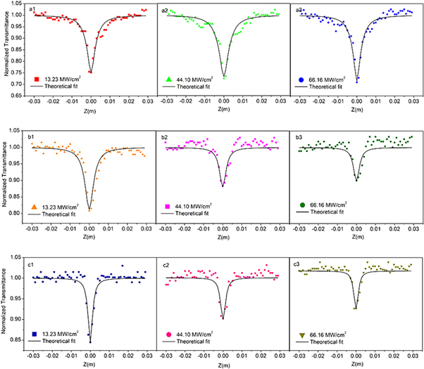
Figure 4. OA Z-scan curves of crystals 1 (a1)–(a3), 2 (b1)–(b3) and 3 (c1)–(c3) at 532 nm under various input intensities.
Download figure:
Standard image High-resolution image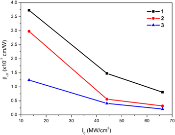
Figure 5. Variation of βeff with respect to input intensities.
Download figure:
Standard image High-resolution imageThe normalized transmittances of single crystals at 66.16 MW cm−2 are presented in figure 6. The obtained βeff are found to be 3.73 ×10⁻⁷, 2.98 ×10⁻⁷ and 1.24 ×10⁻⁷ cm W−1, and the ISAT values are obtained as 6.63 ×10⁹, 3.86 ×10⁹ and 1.80 ×10⁹ W/cm2 for crystals 1, 2 and 3, respectively. Decreased βeff is obtained for increasing Mo/W ratio and a similar trend is observed for ISAT values. The schematic of the proposed NA mechanisms for these single crystals were given in figure 7. All of the single crystals have the same NA mechanism (sequential TPA). On the other hand, their defect states density created differences on the power of NA behaviors. Their defect states density were displayed in figure 7 as dash line. S.G. Singh et all [34] reported five defect centers around 3.1, 2.8, 2.6, 2.0 and 1.7 eV for NaBi(WO4)2 which is represented as crystal 1 in this study. According to figure 5, it was also said that the crystal 2 and 3 have defect states at around 2.32 eV energy region inside the band gap. The observing increasing normalized transmittance (figure 4) can be attributed to lower defect states of crystal 2 and 3 at around 2.32 eV as compared to crystal 1. These lower density of the defect states were filled by OPA and the saturable absorption effect on the NA led to weaker NA behavior as compared to crystal 1. All of the results indicated that the crystal 1 has higher βeff among other single crystals due to its higher defect states. We reported the effect of the defect states on the NA behavior of the single crystals in our previous studies [35–37].
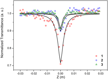
Figure 6. OA Z-scan curves of the crystals 1, 2, and 3 at 66.16 MW cm−2 input intensity.
Download figure:
Standard image High-resolution image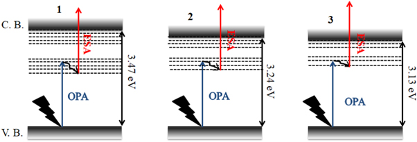
Figure 7. A schematic for the proposed NA mechanisms for the crystals 1, 2, and 3.
Download figure:
Standard image High-resolution imageAn excellent optical limiter for efficient limiting at intense laser beam is composed of FCA, TPA, ESA, nonlinear refraction and nonlinear scattering [38]. As the optical limiters are essential for protecting optically sensitive equipment from hazardous laser light, their development takes great attention [39–41]. An efficient optical limiter limits the transmitted light intensity over its optical limiting threshold and holds it constant, and in this way it protects the sensitive devices. It is well known that a lower optical limiting threshold causes higher optical limiting response. Figure 8 demonstrates the normalized transmission curves as a function of fluence. The distance dependent fluence relation is given by the following equation [42],

where E is the input energy per pulse and t is the pulse duration,  is the beam waist as a function of distance and it can be determined by following the relation for Gaussian beam waist,


where  is the Rayleigh distance,
  is the wavelength of the input light, and
  is the beam waist at focus. Optical limiting thresholds are found to be 5.19 ×10⁻², 3.39 ×10⁻¹ and 4.38 ×10⁻¹ mJ/cm2 for crystals 1, 2 and 3, respectively. It is clearly seen that stronger NA behavior triggers higher optical limiting behavior. Among other crystals, crystal 1 showed stronger optical limiting behavior.

Figure 8. Optical limiting curves of crystals 1, 2 and 3 at 66.16 MW cm−2 input intensity.
Download figure:
Standard image High-resolution image
4. Conclusions
NA and optical limiting characteristics of the NaBi(MoxW1−xO4)2 single crystals for x = 0, 0.5 and 0.75 grown by Czochralski technique were reported in this study. XRD patterns of the crystals presented one peak associated with tetragonal crystalline structure. Linear optical absorption analysis revealed that the bandgap energy decreased from 3.47 to 3.13 eV with increasing concentration of the Mo with respect to W atom in the crystal structure. In addition, the Urbach energy decreased from 0.37 to 0.15 eV with increasing ratio of Mo/W. To investigate the NA behaviors, the OA Z-scan experiments were performed at 532 nm considering OPA, TPA and FCA absorption contributions to NA. Obtained results indicated that all of the studied crystals possess NA behavior. Due to the lower energy of the incident light than the bandgap energy, and the presence of the real intermediate state corresponding to 2.32 eV, the sequential TPA is the dominant NA mechanisms for these crystals. Obtained βeff value decreased from 3.73 ×10⁻⁷ to 1.24 ×10⁻⁷ cm W−1, and ISAT value decreased from 6.63 ×10⁹ to 1.80 ×10⁹ W cm−2 with increasing ratio of Mo/W in the crystal structure. Stronger NA behavior was observed for NaBi(WO4)2 single crystal possessing higher Urbach energy among other crystals. Lower optical limiting threshold was obtained to be 5.19 ×10⁻² mJ/cm2 for NaBi(WO4)2 single crystal which is includes lower Mo/W ratio. All of the results revealed that the bandgap energy can be tunable with the adjustment of the Mo/W ratio to use of the NaBi(MoxW1−xO4)2 single crystals for the optoelectronic application in wide spectral range.
Data availability statement
All data that support the findings of this study are included within the article (and any supplementary files).