
Abstract
Complex-oxide materials are gaining a tremendous amount of interest in the semiconductor materials and device community as they hold many useful intrinsic physical properties such as ferro/piezoelectricity, pyroelectricity, ferromagnetism, as well as magnetostriction and other properties suitable for energy storage elements. Complex-oxides can also be complemented with conventional semiconductor-based devices or used by themselves to realize state-of-the-art electronic/photonic/quantum information devices. However, because complex-oxide materials have vastly different crystalline structures and lattice constant difference compared to conventional semiconductor devices (such as Si or III-V/III-N materials), integration of complex-oxides onto conventional semiconductor platforms has been difficult. Thus, there has been constant efforts to produce freestanding single-crystalline complex-oxide thin films such that these films can be transferred and integrated together with device platforms based on other materials. This review will provide a comprehensive review on single-crystalline complex-oxide membranes technology developed thus far: how they are synthesized, methods to release them from the substrate, and their outstanding properties and applications.
Export citation and abstract BibTeX RIS

Original content from this work may be used under the terms of the Creative Commons Attribution 4.0 licence. Any further distribution of this work must maintain attribution to the author(s) and the title of the work, journal citation and DOI.
1. Introduction
Complex-oxide materials, which are oxide compounds containing more than one metallic element (or one metallic element with at least two oxidation states) [1], are gaining a tremendous amount of interest in the semiconductor materials and device community thanks to their exotic and practical properties not found in conventional Si, Ge, III-V, and III-N based semiconductor materials. The fascinating properties of complex-oxides including ferroic [2–8], pyroelectric [9], piezoelectric [10] and magnetostriction [11], as well as novel interfacial phenomena [12–15] make complex-oxides unique material system to explore emergent phenomena and develop next-generation devices [16–19]. However, due to the large differences in crystal structure and lattice constants, it is difficult to integrate single-crystalline complex-oxide films with conventional semiconductor materials as epitaxy of complex-oxides on conventional semiconductors leads to polycrystalline growth with inferior and degraded material characteristics. In other words, the functionality and integration of complex-oxide materials are hindered by epitaxial limitation. To solve this issue, several novel methods have been developed to allow epitaxial release of ultrathin single-crystalline complex-oxide membranes that can be transferred and heterogeneously integrated onto any arbitrary and desirable platform. These new freestanding single-crystalline complex-oxide membrane creation methods not only allow integration of complex-oxides with conventional semiconductor devices/platforms at the material level, but its freestanding form allows high mechanical flexibility, large surface area to volume ratio, and robust strain tunability via integration on a piezoelectric platform, all of which vastly expand and improve the applicability of single phase complex-oxide materials in areas such as biomedical engineering, catalyst engineering, and flexible nanotechnology. In this review, we will first discuss how complex-oxide materials are epitaxially grown and release from the substrate, discussing recent demonstrations and applications, and concluding with future outlook as shown in the figure 1.

Figure 1. Schematic illustration of representative methods for creating freestanding complex-oxide membranes and their applications. Figure reproduced from [20], Springer Nature Ltd.
Download figure:
Standard image High-resolution image2. Methods of creating freestanding complex-oxide membranes
The methods of creating freestanding single-crystalline complex-oxide membranes are becoming increasingly important for the fabrication of thin, flexible and multi-functional applications based on heterogeneous integration. Complex-oxide materials are typically epitaxially grown by three common epitaxial techniques: (1) Pulsed laser deposition (PLD), (2) (oxide) Molecular beam epitaxy (MBE), and (3) sputter [for a comprehensive overview of epitaxial techniques, please refer to [20]]. Recent epitaxial lift-off and transfer techniques for freestanding single-crystalline complex-oxide membranes enable artificial heterogeneous integration of dissimilar materials as well as the reuse of expensive single-crystalline oxide substrates, significantly lowering fabrication and device costs. In this section, several methods for creating freestanding single-crystalline complex-oxide membranes including chemical lift-off, remote epitaxy and atomically precise spalling are discussed.
2.1. Chemical lift-off
Chemical lift-off is a method of creating freestanding single-crystalline complex-oxide membranes by the epitaxial growth of single-crystalline films on a sacrificial layer and then selectively etching the sacrificial layer through an etchant. The combination of sacrificial layer and etchant is particularly important to obtain high-quality freestanding membranes. A sacrificial layer with appropriate crystal structure, lattice parameters, and stability under subsequent epitaxial growth conditions highly affect the crystalline quality of the freestanding membranes. Etchants with high selectivity reduces damage to the substrate and membrane during the selective etch process and facilitate substrate reusability.
Water soluble layers are good candidates for sacrificial layers due to its sustainability, reliability, and non-aggressive etching (figure 2(a)). Sr3Al2O6 (SAO) [21–36] is a complex-oxide that has been widely used as a water-soluble sacrificial layer for several reasons. First and foremost, it is readily dissolved in water. Second, it has a structure similar to and is highly lattice matched with SrTiO3 (STO), which is a commonly used epitaxial substrate for complex-oxide perovskites. Third, it can be lattice matched with other complex-oxides by substituting the cation of SAO with Ca and Ba. For these reasons, SAO-coated STO has been used to fabricate a variety of freestanding complex-oxide films, including spinel material such as Sr2LrO4 [37]. Lu et al [38] first demonstrated freestanding complex-oxide membranes using water-soluble SAO as a sacrificial layer. As a proof of concept, they created single-crystalline complex-oxide membranes of STO, La0.7Sr0.3MnO3 (LSMO) and their superlattice (SL) by epitaxial growth on a SAO template and simple water treatment (figure 2(b)). The transmission electron microscopy (TEM) image of the transferred superlattice to a silicon substrate showed no structural collapse nor defect formation during the transfer process, suggesting that single-crystalline complex-oxide heterostructures can be fabricated without degradation based on this approach (figure 2(c)). However, there is a relative lack of research in the fabrication of membrane oxides with dissimilar crystal structures such as spinel and garnet crystal structures, which may also mean opportunities for new discoveries.
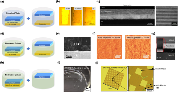
Figure 2. (a) Schematic illustration of water-soluble etching. (b) Optical image of fabricated STO, LSMO, and SL (superlattice of STO/LSMO) freestanding membranes. (c) Cross-sectional high-angle annular dark-field scanning transmission electron microscopy (HAADF-STEM) images of transferred SL on SiO2/Si substrate. Figure reproduced from [38], Springer Nature Ltd. (d) Schematic illustration of non-water-soluble etching. (e) Cross-section TEM image of LFO/SiO2/Si. (f) AFM surface images of the as-grown and transferred LFO film. Figure reproduced from [50], Wiley. (g) Cross-sectional STEM image of the interface between LSMO and Pb(Mg1/3Nb2/3)O3-PbTiO3 (PMN-PT). Figure reproduced from [47], Springer Nature Ltd. (h) Schematic illustration of substrate etching. (i) Optical image of several SRO nanomembranes. (j) Optical image of a SRO nanomembrane transferred to a Si substrate. Figure reproduced from [51], American Chemical Society.
Download figure:
Standard image High-resolution imageWater-insoluble layers are sacrificial layers that use acidic etchants such as HCl [39], NaIO4 [40], and others [41] (figure 2(d)). LaxSr1-xMnO3 [42–46], which uses HCl + KI + H2O as etchant, and SrRuO3 (SRO) [40, 47–49], which uses NaIO4 as etchant, are commonly used water insoluble sacrificial layers. Shen et al [50] demonstrated centimeter-scaled freestanding LiFe5O8 (LFO) oxide thin films by utilizing LSMO/STO substrate. They immersed polyimide/LFO/LSMO/STO into etching solution (HCl + KI + H2O) for approximately 24 h, successfully creating freestanding crystalline LFO. The TEM image of LFO films shows sharp interface and the same thickness as the grown film, indicating that no degradation occurred during transfer (figure 2(e)). Furthermore, the transferred film had a root mean square roughness (RMS) of 0.388 nm while the as-grown film had a roughness of 0.227 nm, indicating that the procedure for dissolving the LSMO sacrificial layer only has a minor effect on the surface morphology of the LFO film (figure 2(f)). Subsequently, Pesquera et al [47] demonstrated freestanding single crystalline LSMO films using SRO as a sacrificial layer. The SRO sacrificial layer was chosen due to its small lattice mismatch with LSMO and selectivity, which allowed it to be etched without damaging the LSMO and STO substrates. Polydimethylsiloxane (PDMS)/LSMO/SRO/STO stacks were floated in NaIO4 solution for several hours and released with clean interfaces. The TEM image of the transferred samples shows clean interface between the SRO and adsorbates (figure 2(g)). However, water insoluble layers have some issues, such as improper acid etchant selection, which may cause damage to the substrate or target films, and the use of acid as an etchant, which may pose safety risks.
There is also a chemical lift-off method that uses the substrate itself as a sacrificial layer [51, 52]. In this method, the target film is grown directly on the substrate, followed by etching of the substrate itself, resulting in a freestanding single-crystalline membrane. If the target film is directly grown onto the substrate, the fabricating process is much simpler than using sacrificial layers. Paskiewicz et al [51] demonstrated freestanding SRO nanomembrane through etching of STO substrate. Patterned SRO was directly deposited on the STO substrate through a MgO mask. After selectively etching the MgO mask, SRO nanomembrane was released by selectively etching the STO substrate, using HF/HNO3/H2O solution. When the substrate and released nanomembrane are transferred to DI water, the SRO nanomembrane floats on the surface of the water (figure 2(i)), allowing transfer to other substrates (figure 2(j)). However, the substrate etching method has some drawbacks, including the fact that it takes a long time to fully etch the substrates and lacks substrate reusability, which leads to higher cost.
The transfer and handling method of freestanding single-crystalline membrane is also an important part of chemical lift-off methods after creating freestanding membrane through chemical etching. The quality of single-crystalline membrane is affected by how it is released, handled, and transferred. To obtain high quality membranes and pristine interfaces between the membrane and target substrate, proper transfer process and handling techniques are required. In a recently published paper, various transfer methods are specifically explained and discussed [53].
2.2. Remote epitaxy
Remote epitaxy is a recently proposed epitaxial growth and layer transfer technique [54, 55]. This method utilizes a host substrate coated with thin 2D materials such as graphene to obtain an epilayer due to the absence of strong bonding with the substrate. Adatoms interact with the substrate even in the presence of a graphene interlayer because graphene on the substrate does not completely screen the potential field of the substrate. In addition, in-plane atoms of 2D materials are held together by strong bonding (covalent or ionic bonding) in the in-plane direction, whereas only weak van der Waals interaction occurs in the out-of-plane direction due to weak binding energy between layers [56]. Thus, remote epitaxy can be utilized as a universal platform for creating freestanding single-crystalline membranes leaving a pristine surface after exfoliation because the epitaxial layer grown on graphene can be easily exfoliated by the weak interfaces. In this sub-section, we will discuss the detailed fabrication process for creating single-crystalline complex-oxide membrane via remote epitaxy as well as technical details for successful remote epitaxy including the formation of 2D interlayer, epitaxy conditions and 2D material-based layer transfer (2DLT).
For remote epitaxy, the following factors need to be considered in addition to the requirements for conventional epitaxy: (1) polarity of the substrate, (2) polarity, thickness and quality of the 2D interlayer, (3) quality of the 2D interlayer and the substrate interface, and (4) preservation of the 2D interlayer during epitaxy process. The remote interaction according to the polarity (ionicity) of the substrate has been reported with compound semiconductor substrates including group III-V, III-N and I-VII [57]. Theoretically and experimentally, it has been shown that GaAs (groups III-V) grows remote epitaxially only on monolayer graphene-coated substate, while relatively high polar LiF (groups I-VII) can grow remote epitaxially even on trilayer graphene-coated substrate. In other words, the potential field penetration through graphene increases as the polarity of the substrate material increases. This result suggests that remote epitaxy can be applied not only to compound semiconductors but also to complex-oxide materials [58]. Meanwhile, research on remote interaction related to the polarity of 2D materials have also been reported with graphene and h-BN, example of non-polar and polar 2D material respectively [57]. For example, GaN (groups III-N) grown on monolayer graphene has an epitaxial relation with the substrate, whereas GaN grown on h-BN has two different azimuthal orientations. In the case of h-BN, it is the result of simultaneous remote and vdW epitaxy with the substrate and 2D material acting as the seed layer. As a result, graphene is used almost exclusively in remote epitaxy due to the transparent to potential field of substrate.
2.2.1. The formation of graphene-coated substrate
The formation of a 2D material on the single-crystalline substrate is a very important factor in remote epitaxy. There are two approaches for forming graphene on the substrate for remote epitaxy: transfer and direct growth. In the transfer approach, semi-dry transfer of epitaxial graphene on SiC and wet transfer of chemical vapor deposition (CVD) grown graphene on metal catalyst are mainly utilized. The single-crystalline monolayer epitaxial graphene is formed at high temperatures by the sublimation of silicon and the rearrangement of carbon in a single-crystalline SiC substrate, a process known as graphitization [59, 60]. In addition, the graphene on SiC can be transferred to any arbitrary substrate of interest via semi-dry transfer method without significant degradation of quality [61, 62]. The semi-dry transfer method begins by depositing a metal stress layer such as Ni on the epitaxial graphene surface. Both an evaporator and a sputter can be used in this procedure, but an evaporator is recommended to avoid damage to graphene induced by energetic plasma. Then, graphene can be exfoliated from the SiC substrate using a thermal release tape (TRT) as a handling layer. The thermal release tape acts like any other tape at room temperature, but when heated to a specific temperature, the stickiness completely disappears. This enables facile transfer process of the exfoliated stack onto a substrate of interest using a hot plate. Following the use of an etchant and a deionized (DI) water rinse, the stress layer is removed, leaving only graphene on the substrate. However, the drawbacks of this method are the high cost of single-crystalline SiC substrates, the high process temperature of graphitization, and the defects on graphene introduced during the transfer process. Another method is to use graphene grown via CVD on a metal catalyst such as Cu foil [63, 64]. Although the metal catalyst can facilitate the formation of graphene at a relatively low temperature, the graphene grown by CVD on foil primarily has a polycrystalline nature despite the recent progress [65, 66]. A wet transfer method is typically used to transfer graphene that has been grown on the surface of a rough Cu foil to the desired substrates [67, 68]. The process is as follows: (1) coating a polymer supporting layer such as poly(methyl methacrylate) (PMMA) on the graphene grown Cu foil, (2) remove Cu foil by floating in Cu etchant, (3) rinse off remaining etchant by DI water, (4) transfer the PMMA/graphene stack to the desired substrate and (5) removal of PMMA using acetone. The wet transfer method, however, may introduce a significant amount of defects, polymer residue, and interfacial contamination which can hinder the remote interaction between the adatom and underlying substrate in comparison to the semi-dry transfer method [69, 70].
On the other hand, graphene can be grown directly on a single-crystalline substrate via CVD without a transfer process. For example, direct growth of graphene on STO [71, 72], Al2O3 [73–75], HfO2 [76], ZrO2 [77], MgO [78, 79] and Ge [80–82] has been reported. As long as high-quality graphene can be grown on a single-crystalline substrate, this approach can offer an ideal template for remote epitaxy because there are no defects or interfacial contamination introduced by the transfer process. However, it is still challenging to precisely control the thickness and uniformity of the grown graphene especially over a large area. The non-uniformity thickness of graphene can lead to failure of remote epitaxy. For instance, thick graphene regions where the potential field of substrate is completely screened may cause growth of a polycrystalline layer rather than single-crystalline epitaxial layer.
2.2.2. The interaction of graphene during remote epitaxy
For creating freestanding complex-oxide membrane via 2DLT (figure 3(a)), it is crucial to prevent graphene from being oxidized or etched during the epitaxy of oxides. To the best of our knowledge, there is a lack of studies on the interaction of graphene under various epitaxy process conditions of complex-oxide materials. Meanwhile, recent advances have improved the robustness of remote epitaxy, providing a versatile platform for creating freestanding complex-oxide membranes. Therefore, we will discuss the recent advances and experimental details for remote epitaxy of complex-oxide materials based on all reported works of remote epitaxy of complex-oxides in the lab around the world (table 1).

Figure 3. (a) Schematic illustration of 2DLT. Figure reproduced from [20], Springer Nature Ltd. (b) Cross-sectional TEM of STO grown on a bilayer graphene-coated STO substrate with ultrathin buffer layer. The image on the right is the fast Fourier transform (FFT) of the epitaxial layer and substate, respectively. (c) EBSD image of the freestanding STO membrane. (d) Optical image of the freestanding membranes. Figure reproduced from [58], Springer Nature Ltd. (e) Schematic illustration of mechanism of ALE. (f) Raman spectrum of graphene before and after ALE. (g) Optical image of the freestanding STO membranes. Figure reproduced from [87], AIP Publishing. (h) Schematic illustration of hybrid MBE (i) Cross sectional HAADF-STEM image of STO grown bilayer coated-STO substrate. (j) Cross sectional HAADF-STEM image of transferred STO membrane on Al2O3. Figure reproduced from [92], AAAS.
Download figure:
Standard image High-resolution imageTable 1. Reported complex-oxides and processes for remote epitaxy.
| Grown epilayer | Substrate | 2D interlayer | 2D synthesis method | 2D transfer method | Epitaxy tool | Comment | References |
|---|---|---|---|---|---|---|---|
| STO | STO | Bilayer graphene | Graphitization of SiC | Semi-dry | PLD | Bilayer graphene and ultra-thin buffer layer are needed | [58] |
| CFO | MAO | Bilayer graphene | Graphitization of SiC | Semi-dry | PLD | Bilayer graphene is needed | [58] |
| YIG | GGG | Bilayer graphene | Graphitization of SiC | Semi-dry | PLD | Bilayer graphene is needed Post-annealing about 850 °C to improve crystal quality | [58, 94] |
| BTO | STO | Monolayer graphene | Graphitization of SiC/CVD on Cu foil | Semi-dry/Wet | MBE | Graphene is immediately etched if ozone is used | [58] |
| VO2 | Al2O3 | Monolayer graphene | CVD on Cu foil | Wet | PLD | Low exfoliation area yield (5%) | [84] |
| LiNbO3 | Al2O3 | Monolayer graphene | CVD on Cu foil | Wet | PLD | There is no mention of exfoliation | [85] |
| STO | STO | Mono-/bilayer graphene | Direct CVD growth | — | PLD | Atomic layer etching is used Ultra-thin buffer layer is needed | [87] |
| VO2 | Al2O3 | Bilayer graphene | CVD on Cu foil | Wet | Sputter | There is no mention of exfoliation | [86] |
| STO | STO | Monolayer graphene | CVD on Cu foil | Wet | MBE | Graphene is immediately etched if ozone is used regardless of buffer layer | [91] |
| BTO | Ge | Monolayer graphene | Direct CVD growth | — | PLD | Ge (110) substrate allows remote interaction | [88] |
| STO | STO | Bilayer graphene | CVD on Cu foil | Wet | MBE | Hybrid MBE is used | [92] |
| LSAT | STO | Monolayer graphene | CVD on Cu foil | Wet | MBE | Hybrid MBE is used | [92] |
Firstly, it is demonstrated that single-crystalline membranes of a wide range of complex-oxide materials including perovskite, spinel and garnet crystal structures have been fabricated based on remote epitaxy [58]. Theoretically and experimentally, it has been shown that the potential field of the substrate penetrates completely up to bilayer graphene, allowing remote interactions. In this work, perovskite STO, spinel CoFe2O4 (CFO) and garnet Y3Fe5O12 (YIG) were grown on bilayer graphene-coated single-crystalline STO, MgAl2O4 (MAO) and Gd3Ga5O12 (GGG) substrates using PLD, respectively. The bilayer graphene on a single-crystalline complex-oxide substrates were formed by semi-dry transfer of epitaxial graphene. It is worth noting that graphene may be damaged during the harsh energetic epitaxy process of complex-oxide materials using PLD. In particular, it has been reported that the STO epitaxy process at high temperatures and oxygen overpressure causes the graphene interlayer to be etched (figure 3(b)). The absence of graphene results in direct bonding between the epitaxial layer and the substrate, significantly reducing the exfoliation area yield and making it difficult to reuse the single-crystalline substrate. This issue was successfully resolved by growing an ultrathin (5–10 nm) STO buffer layer under vacuum at the nucleation stage of epitaxy to ensure preservation of the graphene interlayer (figure 3(b)). Given the constrained oxygen source, there is a possibility that the buffer layer will initially be oxygen deficient. However, it was demonstrated that the composition of the buffer layer was identical to that of the subsequent regions grown in oxygen ambient. It appears that the regions grown in the oxygen ambient supply oxygen to the buffer layer due to long diffusion length of oxygen [83]. Therefore, it would be beneficial to grow a buffer layer as thin as possible in order to form a perfect homogenous stoichiometric epilayer.
The grown STO epilayer was successfully exfoliated from the substrate with a high exfoliation area yield (90%) using a Ni stress layer and a TRT handling layer, and the freestanding membrane showed excellent single-crystallinity, which was confirmed by electron backscatter diffraction (EBSD) (figure 3(c)). On the other hand, it is intriguing to note that during the CFO and YIG epitaxy, graphene was not etched even in the absence of a buffer layer (figure 3(d)). Additionally, it has been reported that when graphene grown on Cu foil via CVD or monolayer epitaxial graphene is used, the remote epitaxy of these three materials results in low exfoliation area yield or damage to the substrate during the exfoliation process. Afterward, a few instances of remote epitaxy of oxides on wet-transferred graphene-coated substrates using PLD [84, 85] and sputter [86] have been reported, but these works either do not mention exfoliation or have very low exfoliation area yield.
Remote epitaxy of complex-oxide based on directly grown graphene on single-crystalline substrates has also been reported [87, 88]. However, it is challenging to grow graphene with the desired thickness due to the random nucleation and growth characteristics of 2D materials. As one method to solving this issue, the thickness of graphene that was grown directly on the substrate was controlled by atomic layer-by-layer etching (ALE) process [87]. The mechanism of ALE is chemical adsorption of an oxygen ion beam to the graphene sheet, followed by physical desorption through an energetic argon ion beam (figure 3(e)). The Raman spectrum of the graphene directly grown on STO substrates before and after several cycles of ALE revealed a gradual improvement in the 2D peak intensity and red shift in the 2D peak position, demonstrating effective thickness control (figure 3(f)) [89, 90]. This led to the successful growth of single-crystalline STO by remote epitaxy on direct growth and ALE processed graphene-coated STO substrate, as well as an increase in exfoliation yield (figure 3(g)).
Meanwhile, unless ozone is used as an oxygen source, remote epitaxy using MBE is known to cause minimal damage to graphene through a relatively gentle growth process. For example, it has been reported that, regardless of the type of graphene used, freestanding single-crystalline BaTiO3 (BTO) membranes can be created via remote epitaxy on monolayer graphene-coated STO substrate [58]. However, in situ x-ray measurement during remote epitaxy of complex-oxide materials via MBE has shown that graphene can be damaged under certain conditions [91]. Based on the measured x-ray results obtained while varying the epitaxy conditions, they were able to confirm that graphene is etched at high oxygen partial pressure. Recently, remote epitaxy of complex-oxide materials using hybrid MBE has been reported [92]. Hybrid MBE is a modification of oxide MBE that uses a titanium tetraisopropoxide (TTIP) source instead of elemental Ti and oxygen source (figure 3(h)). The technique may help prevent damage to graphene during the epitaxy process due to absence of additional oxygen source and make it easy to control the stoichiometry of complex-oxides due to the high vapor pressure of TTIP [93]. The authors demonstrated that wet transferred graphene was not damaged during the epitaxy process by performing remote epitaxy on STO and [(La0.18Sr0.82)(Al0.59Ta0.41)O3] (LSAT) substrates (figure 3(i)). However, in-plane lattice rotation was also observed in the region near the defect in graphene, which seems to have been caused by PMMA residues. They also successfully demonstrated the transfer of grown single-crystalline STO to Al2O3 substrate (figure 3(j)).
2.2.3. Challenges of remote epitaxy
Remote epitaxy is a versatile platform for creating various crystal structure of freestanding single-crystalline complex-oxide membranes, but the method is not without challenges. First, it is difficult to form a uniform, high-quality 2D interlayer on a single-crystalline substrate for remote epitaxy. The transfer method, which has mainly been used in development up to this point, introduces metallic or organic residues as well as defect like tears or holes into the graphene. These factors either limit remote interaction or reduce the exfoliation area yield due to direct epilayer-substrate bonding, making it difficult to produce freestanding single-crystalline membrane. Furthermore, the formation of 2D interlayers using a transfer approach will become challenging for large-area substrates. On the other hand, direct growth approach through CVD is a more suitable method for forming 2D interlayer over large-area. However, it is still difficult to grow a uniform, high-quality 2D material on arbitrary crystalline substrate. Another issue is the damage to graphene that may occur during the epitaxy process. Conventional processes for growing complex-oxides typically oxidize or even etch the graphene on the substrate. It is necessary to take the damage of graphene in remote epitaxy into consideration because it lowers the yield of the exfoliation area and the quality of the grown epilayer. The damage of graphene appears to be influenced by a number of factors, including the epitaxy tool, the type of graphene, the process temperature, the partial pressure of oxygen, the source and the substrate. To ensure successful remote epitaxy, fundamental studies on the interaction of graphene in an epitaxy environment and novel methods to protect graphene during epitaxy process are needed.
2.3. Atomically precise spalling
Atomically precise spalling is a method based on mechanical spalling, a brute force method in which a metal stress layer such as Ni is used for crack propagation (figure 4(a)). The mechanical spalling method cannot precisely control the spalling propagation depth and leaves a rough substrate surface after lift-off due to the relatively crude process. However, the weak interface between the substrate and the epitaxial layer allows for atomically precise crack propagation and reusable clean surfaces of the substrate. This method is especially useful when it is difficult to apply remote epitaxy because the epitaxy process involves a harsh environment that graphene on the substrate cannot withstand.
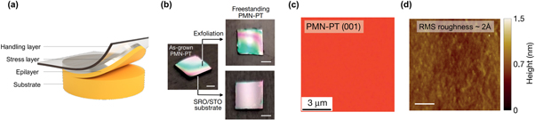
Figure 4. (a) Schematic illustration of atomically precise spalling. Figure reproduced from [20], Springer Nature Ltd. (b) Optical image of as-grown PMN-PT on SRO/STO, freestanding PMN-PT membrane and SRO/STO substrate after exfoliation (The scale bar is 2 mm). (c) EBSD image of the freestanding PMN-PT membrane. (d) Atomic force microscopy image of the freestanding PMN-PT membrane. Figure reproduced from [58], Springer Nature Ltd.
Download figure:
Standard image High-resolution imageIt was discovered that SRO provides a weak interface with PMN-PT [58]. By utilizing the weakly bonded PMN-PT/SRO epitaxial interface, freestanding single-crystalline PMN-PT membrane was successfully implemented by sputtering based on SRO/STO substrate without use of 2D layer (figure 4(b)). The single-crystallinity of the fabricated freestanding PMN-PT membrane was confirmed through EBSD (figure 4(c)). In addition, the RMS roughness of ∼2 Å of the SRO surface after exfoliation demonstrated atomically precise crack propagation (figure 4(d)). Although additional studies on the detailed mechanism of the weak interface of PMN-PT/SRO are needed, this method broadens the types of freestanding complex-oxide membranes that can be fabricated without use of 2D layer.
3. Advantages of freestanding single-crystalline films in membrane form
Various functional properties of complex-oxide films can be coupled through heterogeneous integration and enhanced [95–105] by applying mechanical strain. However, conventional methods based on epitaxial strain have critical limitations in the combination of materials constituting the heterostructure and controlling the strain [106, 107]. Recently, freestanding single-crystalline film in membrane form is allow the alternative methods to control the strain with mechanical bending [108–110], mechanical stretching [111] and tuning the interlayer stress [112]. In addition, since the membrane form is free from the substrate clamping effect, the properties of the complex-oxides are improved. This section introduces the advantages of freestanding single-crystalline complex-oxides in membrane form as an appropriate solution to these drawbacks.
3.1. Declamping effects
The functional properties of complex-oxide films are significantly dampened by the substrate clamping. In particular, mechanical clamping of the rigid substrate restricts the elastic deformation and the movement of the ferroelastic domain wall of the ferroelectric complex-oxide film, which greatly weaken the piezoelectric properties and poling characteristics [113, 114]. Such issues of the mechanical clamping limit the properties of complex-oxide materials for multifunctional ultra-low power devices by constraining the functionality of complex-oxide and the dynamics of ferroelectric switching. Therefore, the freestanding membrane form can improve the key physical properties of complex-oxide compared to the epitaxially grown thin film fixed to the substrate by the so-called declamping effect.
An example is a strain-mediated magnetoelectrically coupled artificial heterostructure fabricated by integrating freestanding single-crystalline membrane form of magnetostrictive CFO and piezoelectric PMN-PT (figures 5(a) and (b)) [58]. The CFO/PMN-PT heterostructure created by stacking freestanding membranes has improved functionality as epitaxial films are not clamped to the substrate. By observing that the freestanding membrane-stacked heterostructure had enhanced magnetoelectric coupling than the case where either material was clamped to the substrate, the declamping effect was unambiguously demonstrated (figure 5(c)).

Figure 5. (a) Schematic of freestanding single-crystalline magnetostrictive CFO and piezoelectric PMN-PT heterostructure based magnetoelectric device. (b) Cross-sectional TEM image of the CFO/PMN-PT artificial heterostructure. (c) The voltage induced across the PMN-PT (δVME) as a function of the alternating-current magnetic field at a frequency of 1 kHz. The inset schematic show the freestanding and the clamped devices respectively. Figure reproduced from [58], Springer Nature Ltd. (d) Schematic of clamped PMN-PT thin film heterostructure. (e) Schematic of freestanding PMN-PT membrane-based heterostructure. (f) Measurement of maximum longitudinal piezoelectric coefficient (d33) using double-beam laser interferometry (DBLI) of clamped and freestanding membrane-based PMN-PT heterostructures. Figure reproduced from [115], AIP publishing. (g) Lattice parameters ratio (c/a) of clamped and freestanding BFO membranes as function of thickness. (h) Polarization-Voltage measurement of 100 nm clamped and freestanding BFO membranes. (i) Switching dynamics of 25 nm thick clamped and freestanding BFO as a function of applied voltage. Figure reproduced from [116], Springer Nature Ltd.
Download figure:
Standard image High-resolution imageRecently, Brewer et al [115] conducted microscopic analysis about the piezoelectric behavior of PMN-PT of the same composition in the form of clamped thin film and freestanding membrane (figures 5(d) and (e)). They measured the maximum d33 piezoelectric coefficient for two samples (∼30 pm V−1 and ∼1100 pm V−1, respectively), and it was confirmed that the piezoelectric coefficient was about 40 times higher in the form of a freestanding membrane than in the clamped thin film (figure 5(f)). In other words, it was shown that the piezoelectric properties of PMN-PT can be significantly improved by the declamping effect in the freestanding membrane form. They also showed that these results are due to the fact that substrate clamping restricts the field-induced rhombohedral to tetragonal phase transition through phase-field simulation.
In addition, Shi et al [116] showed the effect and mechanism of substrate clamping on ferroelectric switching through clamped and freestanding BiFeO3 (BFO) membranes. They demonstrated that the reduction of tetragonality by substrate declamping effect lowered the spontaneous distortion and polarization switching energy of freestanding membranes (figures 5(g) and (h)). Based on these superior characteristics of freestanding membranes, they realized significantly lower switching voltage and improved switching speed compared to clamped films (∼40% reduction, ∼60% improvement respectively), essential for realizing low-power and high-speed ferroelectric electronic devices (figure 5(i)).
3.2. Manipulation and integration
Freestanding membranes also have advantages over conventional epitaxial integration for manipulation and integration of complex-oxide materials. In general, since a sufficiently high temperature condition is required for epitaxial growth, conventional method has limitations in integrating materials having a stable state under very different conditions. In addition, the high temperature makes it impossible to have a clean interface because the layers composed of different materials are mixed by the diffusion. These issues not only limit the heterostructure systems that can be implemented, but also inhibit integration with mainstream semiconductor materials, thereby narrowing the range of application of single-crystalline complex-oxide. On the other hand, freestanding complex-oxide membranes are attracting attention as they can be integrated onto arbitrary substrates at room temperature, making it possible to fabricate various heterostructures, complementary metal-oxide-semiconductor (CMOS)-compatible and flexible complex-oxide devices without suffering the aforementioned issues of conventional method.
Bakaul et al [117] integrated a freestanding ferroelectric Pb(Zr0.2Ti0.8)O3 (PZT) membrane onto a silicon substrate by epitaxial growth of PZT and then transferring it on a silicon-on-insulator (SOI) substrate (figure 6(a)). They fabricated silicon channel field effect transistor allowing control of the channel charge through the polarization state of single-crystalline ferroelectric PZT membrane as a gate insulator (figure 6(b)). The hysteresis of the I–V curve and the rapid change in current demonstrated successful integration of single-crystalline complex-oxide with mainstream semiconductor materials (figure 6(c)). In addition, Singh et al [118] implemented the integration of a freestanding La-doped BaSnO3 membrane into a silicon platform (figure 6(d)). They found that the conventional sacrificial and epitaxial platform had a large lattice mismatch with BaSnO3, resulting in high defect density in the grown membranes. To solve this problem, they developed Ba3Al2O6 as a new water-soluble pseudo-perovskite sacrificial layer and crack-free La-doped BaSnO3 membrane was successfully grown and transferred to a silicon platform, showing superior electrical properties such as high electron mobility (figures 6(e) and (f)). For flexible platforms, many researchers have reported the successful integration of freestanding membranes into flexible substrates such as PDMS. Dong et al [119] demonstrated the integration of freestanding BTO membrane into a flexible PDMS substrate (figure 6(g)) and its excellent ferroelectric properties through piezoelectric response (figures 6(h) and (i)).

Figure 6. (a) Cross-sectional TEM image of transferred ferroelectric PZT on silicon platforms (The scale bar is 5 nm). (b) Schematic of ferroelectric PZT-gated silicon channel transistor fabricated on SOI substrate. (c) The ID-VG (top) characteristics of the transistor shows a clear hysteresis (black curve: drain current ID, blue curve: gate current IG). The L and W are length and width of silicon channel, respectively. Figure reproduced from [117], Springer Nature Ltd. (d) Optical image of crack-free freestanding La:BaSnO3 membrane after transferred onto a silicon platforms with Ba3Al2O6 sacrificial layer. (e) Optical image of Hall bar structure of transferred La:BaSnO3 membranes with Ti/Au electrodes. (f) Mobility and resistivity of as-grown on STO and freestanding La:BaSnO3 membranes. Figure reproduced from [118], American Chemical Society. (g) Optical image of freestanding BTO membrane on flexible PDMS substrate. To test the ferroelectric properties of the transferred membranes, out-of-plane PFM phase images (h) and piezoelectric response loops (i) of BTO membranes transferred to Pt/Si were measured, respectively. Figure reproduced from [119], AAAS.
Download figure:
Standard image High-resolution image4. Novel properties of ultrathin complex-oxide membranes
Reducing the dimensionality of materials to explore new properties is no exception for freestanding single-crystalline complex-oxide membranes. Advanced epitaxy and layer transfer techniques have allowed the fabrication of ultrathin complex-oxide membranes that were previously impossible, and many researchers have reported their interesting properties. In this section, we will provide an overview of the noble properties of ultrathin complex oxide membranes, including enhanced physical, mechanical properties and two-dimensional limit.
4.1. Enhanced functional properties
The functional properties of the complex-oxide film can be improved when it becomes ultrathin. Recently, it has been demonstrated that low-power switching operation through thickness-scaling of ultrathin freestanding single-crystalline BTO films [120]. As a result of measuring the coercive field of the SRO/BTO/SRO heterostructure with different thicknesses of BTO, it was found that the coercive field increases as expected by Janovec–Kay–Dunn (JKD) scaling above 150 nm but has an almost constant value below 150 nm. This phenomenon was explained by the depolarization field by the impact screening electrodes, [121] and since it has a constant coercive field even when the thickness is reduced, its application as a low-power switching device is suggested.
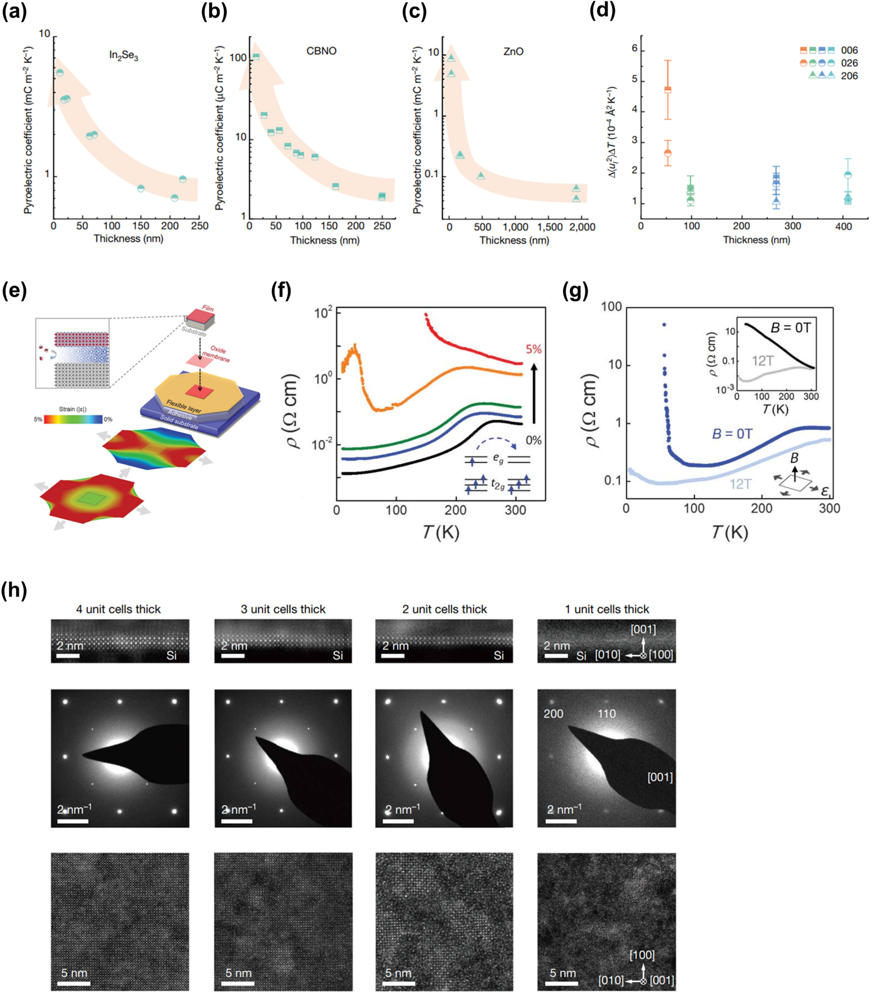
Moreover, Jiang et al [122] reported a study on the behavior of freestanding pyroelectric materials approaching the two-dimensional (2D) limit and dimensionality effect. They investigated three types of pyroelectric materials: van der Waals (In2Se3), quasi-van der Waals (CsBiNb2O7) and ionic/covalent (ZnO), and found that the pyroelectric coefficient rapidly increased as the thickness scaling in all cases (the ratios of pyroelectric coefficients between the thinnest and thickest films: 6 for In2Se3, 55 for CsBiNb2O7 and 207 for ZnO) as shown in figures 7(a)–(c) with Chynoweth technique [123]. The author demonstrated that the dimensionality effect on pyroelectricity was evidenced by electron-phonon renormalization using temperature-dependent XRD measurement from room temperature to 800 °C based on a highly stable CsBiNb2O7 systems (figure 7(d)). The ∆〈ul 2〉/∆T obtained for CsBiNb2O7 with four different thicknesses (410 nm, 268 nm, 98 nm and 53 nm) shows a noticeable improvement at 53 nm, indicating a possible contribution of electron-phonon renormalization in dimensionality effect (the ∆〈ul 2〉/∆T is related to second-order primary pyroelectricity p1 (2), which is the second-order contribution owing to the electron-phonon renormalization). Here, ∆〈ul 2〉 and ΔT represent changes in mean square displacement, temperature respectively. This finding shows the potential for developing high-performance sensors and energy harvesters through enhanced pyroelectric properties through dimensionality effect.

Figure 7. Pyroelectric coefficients as a function of layer thickness for In2Se3 (a), CsBiNb2O7 (b) and ZnO (c), show sharp increased as the scaling in all cases. (d) The ∆〈ul 2〉/∆T obtained for CsBiNb2O7 with four different thicknesses (410 nm, 268 nm, 98 nm and 53 nm). Figure reproduced from [122], Springer Nature Ltd. (e) Schematic of La0.7Ca0.3MnO3 membrane on flexible polyimide platforms. The bottom images represent the finite-element analysis strain profiles of the heterostructure under uniaxial and biaxial stress. (f) Temperature-dependent resistivity of an 8-nm-thick La0.7Ca0.3MnO3 membrane as a function of biaxial strain (black: 0%, blue: 1%, green: 2%, orange: 4%, red: 5%). The inset schematic shows the double exchange interaction between the two Mn sites. Figure reproduced from [126], AAAS. (h) Cross-sectional HAADF images, selected area electron diffraction (SAED) patterns, and planar HAADF images of ultrathin freestanding STO membranes of various thicknesses. Note that single unit cell freestanding membranes can be only measured in low-dose SAED due to their electron-beam-sensitive nature. Figure reproduced from [127], Springer Nature Ltd.
Download figure:
Standard image High-resolution image4.2. Superelasticity and ultraflexibility
In general, complex-oxides easily undergo fracture even with relatively small deformation due to the inflexible nature. However, the dimensionality reduction down to a few atomic layers thickness improves the elasticity/flexibility of complex-oxide membranes as previously studied in other materials [124], enabling the discovery and application of novel phenomena. Dong et al [119] demonstrated improved mechanical properties by transferring nanoscale freestanding BTO membrane to PDMS substrate. By observing the bending test process through in situ scanning electron microcopy (SEM), they showed that the bent state was restored to the initial state over time and fracture did not occur even at ∼10% strain state. The authors reported that these enhanced mechanical properties of BTO are caused by the dipoles that continuously rotate between the ferroelectric nanodomains to avoid mismatch stress that causes fracture.
In addition, Hong et al [125] reported the extreme tensile strain state (uniaxial 8%, biaxial 5%) of a La0.7Ca0.3MnO3 membrane (figure 7(e)). They experimented with varying membrane thicknesses, showing that thick membranes undergo mechanical fracture at relatively low tensile strain, but ultrathin membranes below ∼10 nm can sustain high strain conditions without fracture. The strained membrane showed an unexpected low-temperature insulating phase due to the effect of strain, as well as an increase in resistivity at room temperature and a decrease in the phase transition temperature between ferromagnetic metal and paramagnetic insulator (figure 7(f)). It was also found that magnetic field could cause transition of this strain-induced insulating state to metal along with a large negative magnetoresistance (figure 7(g)).
4.3. Freestanding single-crystalline complex-oxide membranes in 2D limit
The implementation of freestanding single-crystal complex-oxide membranes of nearly fundamental smallest size (monolayer, single unit cell thick) and its characteristics are of major interest to researchers. Hong et al [126] reported on the dimensional limit of crystalline phases of the complex-oxide membrane through epitaxially grown single-crystalline STO of few unit cells thickness using PLD. They found that although the STO film is single-crystalline in all cases, the transferred STO membrane loses its crystallinity when the thickness is reduced below the certain critical thickness (∼five unit cells thick). That is, it was found that STO below the critical thickness undergoes crystalline to amorphous transition during the transfer process. They explained that this unusual phase transition occurs due to the free energy caused by bond breaking during the transfer process based on the Berezinskii-Kosterlitz-Thouless (BKT) theory. The free energy is released when the sacrificial layer is dissolved. The amount of energy is about few electron volts, which appears to be sufficient to affect the stability of 2D crystalline order of ultrathin STO membranes, resulting in structural transition.
Meanwhile, Ji et al [127] showed freestanding single-crystalline complex-oxide membranes of almost down to a single unit cell thickness, well below the critical thickness at which the previously reported crystal lattice collapse occurs. They grew and transferred single-crystalline STO and BFO films from four to one unit cell thickness by MBE and confirmed the high crystalline quality of the membranes as shown in figure 7(h). Similar to the case of graphene [128], it was explained that ripples and roughening of membranes help stabilize the crystalline order at the 2D limit of ultrathin freestanding membranes. Although further research is needed on the conditions, methods and mechanisms that can fabricate monolayer freestanding membranes, these results suggest that there is no limit to the thickness of freestanding single-crystalline complex-oxide membranes that can be fabricated, and furthermore, pave the way to explore new phenomena on ultrathin freestanding membranes of fundamental thickness [129–131].
5. Applications of heterogeneously integrated membranes
Recently, complex-oxide membrane-based heterogeneous structures have been used in various next-generation electronic and optoelectronic devices thanks to the development of epitaxy and fabrication methods. The epitaxial lift-off and transfer technologies have demonstrated that complex-oxides with unique functionalities can be successfully integrated on flexible as well as conventional semiconductors platforms. Thus, complex-oxides can be either integrated with conventional CMOS-based devices or used by themselves to implement state-of-the-art electronic and optoelectronic devices via artificial heterostructures. In this section, we review recent progress in complex-oxide membrane-based applications, such as FETs, memory devices, sensors, harvesters, and resonators.
Silicon-based CMOS technology suffers from leakage power dissipation and reliability issues due to short channel effect and gate tunneling caused by scaling. The heterostructures of 2D materials and complex-oxides are receiving great attention due to their functionality and feasibility for high-performance electronic devices. The 2D materials have excellent electrical and mechanical properties and are known to be suitable next-generation channel materials. However, it was difficult to integrate it with high dielectric constant (high-κ) because nucleation sites could not be provided due to the characteristics of the 2D materials without dangling bonds on the surface, and defects could occur on 2D material during the growth. Without these concerns, freestanding single-crystalline high-κ complex-oxide membrane can be easily integrated with 2D materials. Yang et al [132] reported the facile integration of 2D flake with high-κ complex-oxide and their sharp interface using freestanding STO flake obtained via sacrificial SAO-based epitaxy and chemical lift-off and deliberately rupture (figure 8(a)). They also developed a high-performance MoS2-based n-type field effect transistor with a high Ion/Ioff ratio and near-ideal subthreshold swing through the integration of high-k STO and 2D flakes (figures 8(b) and (c)).
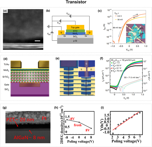
Figure 8. (a) Cross-sectional HAADF-STEM image of an STO/MoS2 heterostructure interface (The scale bar is 2 nm). (b) Schematic of graphene-contacted MoS2 channel Field effect transistor with STO as a gate insulator. (c) Double-sweep IDS-VG (top) characteristics of the device. Figure reproduced from [132], Springer Nature Ltd. (d) Schematic of MoS2 channel Field effect transistor with STO as a gate insulator. (e) Optical image of fabricated devices (The scale bar is 100 μm). The inset shows enlarged image of the white dashed area, where G, S, and D represent gate, source, and drain respectively (The scale bar is 10 μm). (f) ID-VG characteristics of the device. Figure reproduced from [133], Springer Nature Ltd. (g) Cross-sectional TEM images of the ferroelectric PZT/AlGaN/GaN HEMT device. (h) 2DEG density of the fabricated device as a function of poling voltage using Hall measurements. (i) Threshold voltage (Vth) of the fabricated device as a function of poling voltage. Figure reproduced from [134], AIP publishing
Download figure:
Standard image High-resolution imageSubsequently, Huang et al [133] demonstrated large-scale applicability of the heterostructures of 2D material and complex-oxide by integrating CVD-grown 2D film and complex-oxide membrane to fabricate a similar device with comparable electrical characteristics (figures 8(d)–(f)). These examples show the possibility of integrating complex-oxides with various functional properties as well as high-κ with 2D materials in near the future. In addition to 2D materials, functional single-crystalline complex-oxide membranes can be utilized in GaN-based high electron mobility transistor (HEMT) for reconfigurable power and radio frequency (RF) applications. Since the two-dimensional electron gas (2DEG) density in the AlGaN/GaN heterostructure highly affects the performance of devices, heterogeneous integration of ferroelectric materials and polarization engineering are intuitive ways to realize reconfigurable HEMT. Chen et al [134] reported ferroelectric/AlGaN/GaN HEMT using a freestanding PZT membrane through sacrificial LSMO-based epitaxy and chemical lift-off with clean interface (figure 8(g)). The change of carrier density dependent on the poling voltage demonstrated that the two-dimensional electron gas (2DEG) density of the ferroelectric HEMT were tunable with the polarization state of the ferroelectric membrane (figure 8(h)). The threshold voltage shifts up to ∼4V according to poling voltage showed the modulation ability and feasibility of reconfigurable ferroelectric/GaN HEMT (figure 8(i)). Further works, including structural optimization and integration of other ferroelectric materials such as BTO, promise emerging high performance GaN HEMT application [135–137].
For memory applications, ferroic complex-oxide materials are mainly used because their reversible polarization properties enable information storage. The freestanding membrane-based heterostructure enables facile integration of single-crystalline complex-oxide materials with enhanced ferroic properties and conventional CMOS technology and flexible platforms for next-generation memory devices with high scalability and non-destructive readout.
An example is a ferroelectric tunneling junction (FTJ), a non-volatile device that utilizes the modulation of the tunneling current according to the polarization state of thin ferroelectric material [138]. Lu et al [139] reported freestanding BTO-based FTJs on to silicon by transferring an epitaxially grown heterostructure (figure 9(a)). They epitaxially grown water-soluble SAO, ferroelectric BTO and conductive LSMO on STO substrate with PLD, and then fabricated a device on silicon via chemical lift-off-based membrane transfer method and electrode patterning. The ferroelectric properties of the transferred BTO allowing switchable polarization with applied voltage were probed by the PFM phase map (figure 9(b)). The resistive switching characteristics with ∼100 on-off current ratio of the implemented FTJs demonstrated the ability to store clearly distinguishable binary logic states (figure 9(c)). Based on a similar approach, flexible FTJ fabricated on flexible platforms such as polyethylene terephthalate (PET) with a freestanding single-crystalline complex-oxide membranes have also been reported [140]. Another example is a ferroelectric domain wall (DW) memory that stores information via a reconfigurable conductive ferroelectric domain wall [141]. Sun et al [142] fabricated non-volatile ferroelectric DW memory on a silicon platform using freestanding single-crystalline ferroelectric BTO membrane (figure 9(d)). They reported that in-plane ferroelectricity appeared in freestanding BTO membrane due to 90° polarization rotation caused by strain relaxation and depolarization field during the release process (figure 9(e)).
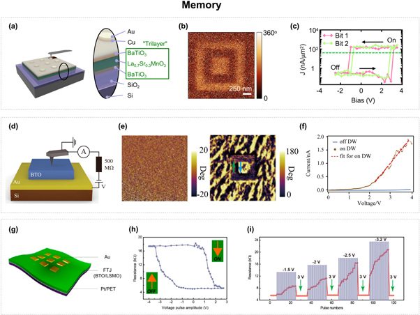
Figure 9. (a) Schematic of freestanding BTO-based FTJs (Cu/BTO/LSMO) on silicon substate. (b) Out-of-plane PFM phase map of the top BTO membranes. (c) Tunnel current measured at 0.2 V after applying gradually incremented and decremented pulsed bias ranging from −2.5 V to +3.5 V clearly shows resistive switching behavior of the devices. Figure reproduced from [139], American Chemical Society. (d) Schematic of freestanding BTO-based DW memory on silicon substate. (e) In-plane PFM phase map of the BTO before (left) and after (right) transfer. (f) I–V characteristics of DW memory device in on and off state. Figure reproduced from [142], Springer Nature Ltd. (g) Schematic of freestanding FTJ-based flexible memristors on PET substrate. (h) The hysteresis of the resistance after applying voltage pulse shows the memristive properties of the fabricated flexible device (reading at 200 mV). (i) The response of the resistance state of the device to multiple SET voltage pulses (0.5 μs) and 3 V ReSET pulses (100 μs). Figure reproduced from [146], American Chemical Society.
Download figure:
Standard image High-resolution imageSince conductive DWs normally require in-plane ferroelectric components, the polarization rotation phenomenon is key to freestanding BTO membrane based DW memory [143]. The electrical characteristic of fabricated DW memory device has demonstrated its potential via a high on-off ratio of ∼103 (figure 9(f)). In addition to the successful information storage of binary logic states, non-volatile memory with continuous tunability of their states could be utilized as memristive devices for neuromorphic computing [144]. With the recent need to process large amounts of data caused by the renaissance of artificial intelligence, the continuous shuffling between memory and processor in conventional computing architecture is limited by von Neumann bottleneck, and thus memristor-based brain-inspired computing architectures are attracting attention to alleviate these issues [145]. Luo et al [146] fabricated BTO/LSMO FTJ-based memristors on flexible PET substrates via freestanding single-crystalline membranes (figure 9(g)). The clear hysteresis of the resistance with the applied voltage pulse amplitude shows the memristive properties of the FTJ, which is probably due to the ferroelectric domain reconfiguration of BTO by the voltage pulse (figure 9(h)). They demonstrated that it is possible to successfully modulate the resistance state of the device by applying multiple pulses of different amplitude (figure 9(i)). In a similar approach, the fabrication of FTJ-based memristor using freestanding BFO/LSMO membranes was also reported [147]. These studies suggest the feasibility of non-von Neumann computing systems based on freestanding complex-oxide membranes in the future [148].
The functional properties of complex-oxide membranes can also be utilized for sensor and harvester applications. Li et al [149] fabricated a tactile sensor on a flexible PET substrate based on a freestanding VO2 membrane using ZnO sacrificial layer (figure 10(a)). They used a freestanding membrane form to take full advantage of the piezoresistive properties of the strain-controlled VO2 resistance as a sensor [150]. The fabricated device clearly showed the change in the resistance value according to the strain applied by bending, and the gauge factor (the ratio of the change in resistance to the applied strain) has a maximum value of ∼1100 when −0.05% compressive strain is applied (figure 10(b)). The electrical response to strain by periodic bending and release demonstrated reliable operation of the sensor (figure 10(c)). Also, Song et al [151] fabricated a pyroelectric photodetector based on ferroelectric BTO (figure 10(d)). Transparent indium tin oxide (ITO) was selected for the top electrode of the device so that the irradiated light could be transmitted to BTO. Ultraviolet (UV) light irradiation causes a change in surface temperature, and the light-induced temporal temperature gradient is converted into an electrical signal by pyroelectric properties. The measured pyroelectric current signal under 365nm light illumination shows the UV light detection behavior of the fabricated device (figure 10(e)). The charge density obtained by integrating in the time domain of the pyroelectric current shows that the freestanding device has a much larger value than the device fabricated on the substrate, and the improvement appears to be a result of a change in heat transfer rate depending on whether a substrate is present (figure 10(f)). In addition to the sensor, a complex-oxide-based energy harvesting device has also been reported. Zhang et al [152] fabricated a piezoelectric ultrasound energy harvester encapsulated in biocompatible PDMS based on single-crystalline Sm-doped Pb(Mg1/3Nb2/3)O3-PbTiO3 (Sm-PMN-PT) (figure 10(g)). The measured output voltage with ultrasound transducer shows the operation of fabricated devices depending on the intensity of the input ultrasound (figure 10(h)). In addition, the electrical output characteristics under different external load resistance show that the device has a maximum instantaneous power density of ∼1.1 W cm−2, which is much larger than previously reported values (figure 10(i)). To demonstrate feasibility for deep brain stimulation, the authors performed in vivo electrophysiological experiments to stimulate periaqueductal gray (PAG) by implanting the device under the scalp of rats (figure 10(j)). The recorded local field potential (LFP) signal of with and without implanted device showed successful activation of the PAG of the implantable Sm-PMN-PT energy harvester (figure 10(k)).
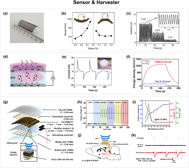
Figure 10. (a) Optical image of freestanding VO2 membrane on flexible PET substrate. (b) Gauge factor as a function of strain applied by inward and outward bending. (c) Electrical response of the fabricated device upon periodically loading-unloading strain (−0.3%, −0.2%, and −0.1%) under a frequency of 1 Hz (the signal measured at 1 V). The inset shows a magnified view of the periodic peak in the blue rectangle. Figure reproduced from [149], Wiley. (d) Schematic of pyroelectric photodetector based on ferroelectric BTO. (e) Output current of the fabricated device under 365 nm UV light of 247 mW cm−2. The inset image shows the freestanding device under UV illumination. (f) The charge density of the device on the substrate (S) and in freestanding (FS) respectively. Figure reproduced from [151], Wiley. (g) Schematic of piezoelectric ultrasound energy-harvesting device based on Sm-PMN-PT. (h) The output voltage signal of fabricated device under 1 MHz ultrasound with different intensities. (i) The output voltage, current, and power of device under different external load resistance under 1 MHz ultrasound with 2.5 MPa. (j) Schematic of in vivo experiment for deep brain stimulation by implanting the device under the scalp of rats. the stimulating and recording electrodes were both placed in the PAG brain area. (k) In vivo recorded LFP signal under 1 MHz ultrasound without implanted device (US & no device), and with implanted device (US & device). Figure reproduced from [152], AAAS.
Download figure:
Standard image High-resolution imageAnother application for freestanding complex-oxide membranes is resonators and actuators. Davidovikj et al [153] fabricated a nanomechanical resonator by transferring a freestanding complex-oxide membrane onto a silicon substrate with cavities using the SAO sacrificial template (figure 11(a)). The optothermal actuation of the fabricated device by blue laser was successfully observed through continuous He-Ne laser, and the frequency spectrum of the fabricated resonator shows a clear mechanical resonance (figure 11(b)). The authors have demonstrated that several structural phase transitions can be detected through the resonator. They observed that the temperature-dependent resonance frequency trend of the STO membrane-based resonator changes at the temperature at which STO undergoes a structural phase transition (figure 11(c)). Furthermore, Lee et al [154] used a freestanding complex-oxide membrane as a self-sealing platform for pressure sensor application. They demonstrated that the adhesion between complex-oxide membrane and SiO2 can be improved through simple annealing process using the previously studied freestanding membrane-based resonator. Similar to the previous study, freestanding membranes were transferred to SiO2/Si substrate with cavities, showing optothermal actuation behavior and resonance peaks under laser illumination (figure 11(d)). They measured the response of resonance frequency according to the pressure change of the device before and after the annealing process through the resonator (figure 11(e)). The enhancement in the gas permeation time constant(τp) after the annealing process demonstrated the self-sealing effect of the device. The authors found that similar devices fabricated on oxygen-free substrates did not show this improvement, suggesting that self-sealing results from the improvement of adhesion through the reaction of oxygen-rich substrate with dangling bonds of complex-oxide membrane by annealing process (figure 11(f)).

Figure 11. (a) Schematic of nanomechanical resonator based on freestanding complex-oxide membrane onto a silicon substrate with cavities. (b) Frequency spectrum of the STO membrane-based resonator showing the resonant frequencies of the fundamental resonant mode (f0) and the second resonant mode (f1). (c) Fundamental resonant frequency as a function of temperature. The inset shows a plot of the temperature range from 4K to 200K. Figure reproduced from [153], Springer Nature Ltd. (d) Frequency spectrum of the device with fitting curves in red. The inset shows an optical image of a freestanding SRO membrane on a circular cavity of SiO2/Si (scale bars are 10 μm). (e) The pressure response of the fundamental resonant frequency of the device before and after the sealing process by annealing. (f) Schematic of the possible mechanism consistent with the experimental results. Before annealing, there is a vdW gap due to a dangling bond, but a strong bond between the membrane and oxygen of the substrate is formed by annealing. Figure reproduced from [154], American Chemical Society. (g) Schematic of the graphene and freestanding BTO based resonator on silicon platform. A red laser is used to detect displacements of the device. (h) Frequency spectrum showing piezoelectric actuation using alternating voltage applied to upper graphene while grounding the lower graphene and substrate. (i) The magnitude and phase of the BTO membrane measured while sweeping the alternating frequency. The red and blue curves indicate measurements were taken after up and down polling by 12.5 V bias, respectively. Figure reproduced from [155], Wiley.
Download figure:
Standard image High-resolution image
A piezoelectric resonator based on heterogeneous integration of freestanding ferroelectric BTO membrane and graphene has also been reported [155]. A device with a BTO membrane between graphene electrodes was fabricated on SiO2/Si with cavities for measurement of piezoelectric actuation using a laser (figure 11(g)). The author confirmed the piezoelectric actuation and resonance peak of the device at room temperature by applying alternating voltage to the BTO membrane (figure 11(h)). In addition, it was demonstrated that the ferroelectric switching of the BTO caused a 180° phase shift and a change in the resonant frequency of the device (figure 11(i)).
6. Challenges and outlook
Although methods to create freestanding single-crystalline complex-oxide membranes have had tremendous development over the past five years, there are still many challenges to overcome. In terms of chemical lift-off techniques, many sacrificial layers are only compatible with complex-oxide materials having perovskite crystalline structures such as STO. Thus, other crystalline structures such as spinel and garnet complex-oxides still require a suitable sacrificial layer to be found. Additionally, chemical lift-off is not scalable since large wafers can take up to several days for complete etch. Although remote epitaxy technique alleviates some of these issues, techniques to obtain and transfer pristine monolayer graphene onto arbitrary substrates still needs to be developed. Since epitaxy is an atomic scale process, even the smallest defects and residues can lead to polycrystalline growth, which significantly reduces the performance and physical characteristics of these ultrathin films. Similarly, spalling with atomical precision only seem to work on heterostructures with epitaxial layers constituting large lattice mismatch or atomic composition. Moreover, handling these atomically thin membranes at the wafer scale and heterogeneously integrating it onto other semiconductor platforms is an open challenge to be solved. Atomically bonding freestanding films at the wafer-scale, ensuring absolutely no air voids is yet to be demonstrated.
Nevertheless, epitaxial exfoliation and heterogeneous integration of dissimilar single-crystalline membranes is the future of electronics. It allows creation of novel electronic and photonic devices with superior performance than conventional devices by allowing the engineer to choose the most optimal material, whether it be bulk 3D materials, atomically thin 2D materials, semiconductors, complex-oxides etc, rather be constricted by materials that are lattice matched to the substrate. Ultimately, it is a pathway towards realizing ubiquitous electronics that will lead to ultrasmall electronic devices with multifunctionality such as sensing, data processing, memory, wireless communication to be integrated onto any environment.
Acknowledgments
This research was supported by the National Research Foundation of Korea (NRF) (grant no. 2022M3D1A2085228). The authors also acknowledge support from the Department of Electrical and Electronic Engineering at Yonsei University.
Data availability statement
No new data were created or analysed in this study.