

Abstract
We model and study the electronic and transport properties of a planar 2D superlattice (PSL) structure containing laterally arranged alternating ribbons of Transition Metal DiChalogenides (TMDC). Within governed effective Hamiltonian we derived adopted transfer matrix formalism to obtain dispersion relation and electronic band structure with wave functions, transmission probability and Fano spectrum. Surprisingly, spin orbit coupling has considerable opposite effects on valence bands shift in TMDC-PSL that is blue and red for k and k' valleys, respectively. The amount of contribution of each ribbon determines the transmission spectrum and the transport feature. We observed that outside the band gap, the Fano factor changes from 1 to smaller values gradually, that indicates the ballistic transport. To give real aspect to our model, the effect of structural disorder and defect are addressed in details. Interestingly, we found that main gap is not dependent on structural disorder and electron incident angle. Our study presents an efficient way to control the key parameters in conductivity and band structure of TMDC-PSL in the view of optoelectronics applications.
Export citation and abstract BibTeX RIS
1. Introduction
Two dimensional materials with atomic thickness such as graphene, Boron Nitride, phosphorene present themselves as promising materials for next generation electronics and photonics due to unique optoelectronic properties [1–19]. One of most important members of 2D materials are transition metal dichalcogenides (TMDCs) that has been emerged as complementary to graphene based electronics. 2D-TMDCs (MX2, with M = Mo, W, etc., and X = S, Se, etc.) are quasi layered materials with strong covalent bonding which are typically produced through liquid-phase exfoliation from their bulk counterparts. Using them with graphene in device application is not also because of similar lattice geometry of monolayer TMDCs (ML-TMDCs) but also due to comparable electronic, optical, chemical, thermal and mechanical features with graphene [20–24].
2D features of TMDCs are basically different from bulk ones, such as crossover from indirect to direct band gap as the thickness drops to one monolayer which is composed of single layer transition metal atom (M) embedded between two atomic layers of chalcogenide atom (X) in a trigonal prismatic structure [16].
Inversion symmetry in these structures is broken due to occupation of two sublattices by single M atom and two X atoms. Besides, broken central symmetry causes strong spin-orbit coupling that splits valance bands and partially conduction bands in monolayer TMDCs [25]. Properties of TMDCs can be modulated by different methods for example, strain [26, 27], external electric field [28] and doping [29].
Recently, heterostructure of TMDCs provide a new route for tuning electronics properties [5, 30, 31]. Bringing different monolayer TMDCs features together in a heterostructures paves a path way for next generation nanoelectronics and nanophotonics devices [32, 33]. However, there is a drawback in Vander wales heterostructures composed of TMDCs monolayers that creates a challenge in implementing them for applications: direct band gap characteristic disappears in these structures. Among vertical heterostructures reported so far, only MoS2/WSe2 has direct band gap that easily switch to indirect band gap by very small disorder [34]. In fact, all MoS2/MX2 superlattices illustrate indirect band gap characteristics. In order to overcome this inefficiency, planner heterostructure has been attracting interests. Importantance of this new kind of heterostructures is demonstrated as essential needs to laterally integrating 2D materials in 2D electronics.
Planner superlattices with two dimensional confinements can be realized by stitching 2D semiconductors or alternatively sandwiching them between two materials in a plane [35–45]. In particular, structural similarities in TMDC semiconductors makes the high quality planar heterostructure with atomic sharp interfaces [36–42]. Multi-heterostructures or planar superlattices with almost a few nanometers width and compassing lots of interfaces in a small length has not been reported yet and has been remained a big challenge for researchers who are exploring high efficiency solar cells or other electronic devices based on 2D TMDCs [46].
Recently, embedded sub-nanometer 2D channels have shown a great potential of proceeding future electronics and enhancement of solar cells efficiency. Two research groups independently reported the growth of planar quantum wells with less than 2nm width and high quality inside TMDCs semiconductor [47, 48]. Partial difference in atomic bonding length between different neighboring monolayers of TMDCs creates different hexagons in MoS2 and WSe2 in the way that by increasing the number of adjacent dislocations in WSe2, channels with width of less than 2nm are created and planar superlattice pattern is appeared including WSe2 and MoS2 [42, 47]. Therefore, it can be expected that similar growth mechanism can be employed and adapted for making 2D multi quantum wells systems or planar superlattices with the ability of tuning the width of ribbons. To the best of our knowledge, there are a few works on studying planar TMDCs superlattices, theoretically. For example, in Ref. [49] authors studied tunability of direct and indirect band gap of MoS2/WSe2 planar superlattice through density functional theory approach (DFT).
Motivated by these studies, in this paper we study the electronic band gap structure and transport properties of planar TMDCs structures with main focus on conductivity and Fano factor. By adopting transfer matrix formalism, we will obtain electronic band dispersion and wavefuctions from governed 2D Dirac like Hamiltonian. We will evaluate the effect of incident charge carriers angle, and geometrical parameters. In order to bring our model closer to reality [47, 48], we consider disorders and defect effects. We also find wavefunctions or probability amplitude that provides a tool to predict transport and even optical response of TMDCs superlattices. Our analytical approach not only is simple to follow but also gives results with very good consistency with that obtained by atomistic calculations within DFT.
Paper is organized as follows. The model superlattice and analytical method to get band dispersion and Fano spectrum are presented in section2 then in section 3 discussions on obtained results is provided in details. Finally, we will conclude and summarize our work in section 4.
2. Model and method
2.1. Extended transfer matrix formalism
The behavior of electrons in ML-TMDCs is governed by 2D Dirac-like equation that reads [50]:

 are well known Pauli psedu spin matrix and
  is momentum operator in x−y plane.
  is unit operator, a and t are lattice constant and effective hopping integral. Δ, 2λ, s and τ correspond to the direct band gap, spin-orbit splitting at the band extrema, s = +1(−1) indicate spin index and τ = +1(−1) is valley index attributed to K (K').
Spin orbit coupling (SOC) is appeared in single layer of TMDCs due to breaking symmetry results in removing degeneracy in band extrema and creating splitting that is significant in valence band extremum (about a few hundreds of meV). Third term in equation 1 shows SOC effect.
Hamiltonian operates on a two component pseudo-spinor wavefunction as ψ = (ψA , ψB ), where ψA = (x, y), ψB = (x, y) are the envelope functions for two sublattices in TMDCs. One can write ψA,B (x, y) = ψA,B (x)eikyy because of translational invariance in y direction. Equation (1) can be decomposed to two coupled following equations as:


where kA,B
is defined as  and
and  E is incident energy of electrons. Figure 1 depicts schematic structure of our model for a planar superlattice. Regions A, B indicate two different ML-TMDCs that are MoS2 and WSe2 in our work. Structural parameters and incident angle of carriers are shown clearly.

Figure 1. (a) Schematic view of a planer superlattice structure consisting of various ML-TMDCs , A, B on the  plane;
  and
and  are the angles of incident and exit of the carriers that pass through the structure, respectively,
 in the inset is the carrier angle in jth layer. (b) Schematic representation of a planer superlattice showing the position of ML-TMDCs atoms, and planer superlattice Parameters based on lattice constant (
 ) of ML-TMDCs Semiconductors.
Download figure:
Standard image High-resolution imageFrom equation (2) it is straightforward to obtain following equations:


 in jth layer. Assuming
 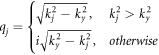 is the x component of the wavevector in the jth layer. One can suggest following answers for set of two coupled equations (3a
) and (3b
) as:
is the x component of the wavevector in the jth layer. One can suggest following answers for set of two coupled equations (3a
) and (3b
) as:


a and c (b and d) are forward (backward) spinor components. From combining equations (4) and (2) it is straight to obtain wavefunctions ψA,B (x) as:


In order to connect the wavefunctions, ψA,B
(x) at arbitrary points of x direction in jth layer, we will consider the basis as  and assume that these basis can be written as:


Now, wavefunctions ψA,B (x). can be rewritten as:

where:

Pj
and θj
 are
are  and
and 
 respectively. The relation between basis at two points of
  and
and  can be easily obtained as:


From equations (9) and (8), adopted or extended transfer matrix,  can be obtained that connects wavefunctions
  and
and 
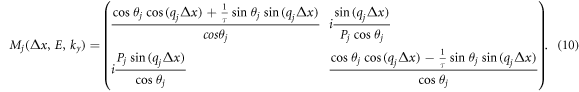
Given the components of the matrix M, it can be shown that determinant of Mj(Δx, E, ky ) is unique, det[Mj(Δx, E, ky )] = 1.
2.2. Wavefunction, transmission and reflection coefficient
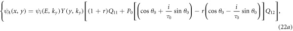
In order to determine two-component wavefunction at each arbitrary point of x, it is necessary to have information about it at initial point of x0,  Having boundary conditions in hand, depicted in figure 1, we assume free electron with energy of E from x0 < 0 region enters the planar superlattice at the angle of θ0. In this region (x0 < 0), the final wavefunction will be a combination of incident and reflected waves so that at the incident point of the superlattice (x = 0) the wavefunction component ψA
(x0 = 0) is re-written as:
Having boundary conditions in hand, depicted in figure 1, we assume free electron with energy of E from x0 < 0 region enters the planar superlattice at the angle of θ0. In this region (x0 < 0), the final wavefunction will be a combination of incident and reflected waves so that at the incident point of the superlattice (x = 0) the wavefunction component ψA
(x0 = 0) is re-written as:

ψi (E, ky ) is the electron incident wave packet at x = 0, and ψr (E,ky ) = rψi (E,ky ) where r is reflection coefficient. From equations (5a ) and (6a ), it is easy to obtain φ1(0) = (1+r)ψi (E,ky ) and φ2(0) = (1−r)ψi (E,ky ). Using equation (8) ψB (0) is obtained as:

And finally:

By defining t as total transmission coefficient and by using equation (7) in final point of superlattice (x = xe ) we have:

θe is exit angle at the end of the superlattice. X is called transfer matrix that connects wavefunction at incident point to that of the end of superlattice as:

Since the whole structure of the superlattice is composed of N ribbons with width of wj , then one can construct X as multiplying matrices Mj as:

Considering detMj = 1, it is very easy to reach detX = 1. Therefore, using equations (13)–(15) reflection and transmission coefficient (r, t) for whole structure can be calculated. In particular, for τA,B = ±1, r and t are obtained as:


In order to determine wavefunction ψA.B (x) at arbitrary point of x between xj−1 and xj (xj−1 < x < xj ) in jth layer, we must obtain connection matrix that connects wavefunction ψA.B (x0) at initial point of x0 to ψA.B (x) as:

where Δxj = x−xj−1 and matrix Q, connection matrix can be written as:

In fact, matrix Q is composed of transfer matrix of (j − 1) ribbons or layers with width of wi and jth layer with width of Δxj .
Also, we can determine wavefunction of each sublattices as:


As Qmn 's are the elements of the matrix Q.
To complete our theoretical approach, we also work on y direction of wavefunction that is obtained by multiplying 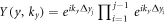 to
to 

 is defined according to figure 1 as
  and
and  So final wavefunction reads:
2.3. Dispersion relation
Finally, it is straightforward to get dispersion relation for TMDC-PSL very similar to the known approach followed in conventional periodic structure within Bloch theorem. From equation (10) and knowing that  we obtain dispersion relation as:

where Λ = wA + wB .
2.4. Conductance (σ), Fano factor (F)


3. Results and discussion
In this section, we like to investigate the influence of different parameters on band structure with transport properties in planner TMDC superlattice (TMDC-PSL) by using adopted transfer matrix method presented in previous section. The size of unit cell is Λ = wA + wB and wA = NA zA , wB = NB zB are width of A and B ribbons. zA,B is the size of unit cell in x direction (in-plane growth direction) listed in table 1 and NA,B is the number of hexagons. We take the length of structure in x direction as Lx = 51Λ + wA and Ly in y direction (see figure 1). First, we investigate the electron band structure and transmitivity of the structure. Figure 2(a) depicts the band structure of TMDC-PSL containing alternating layers or ribbons of WSe2 and MoS2 where wA = 5zA and wB = 5zB , respectively, with(without) spin-orbit coupling, SOC, effect, shown by blue(red) curves. Energy gap without SOC has been obtained as 1.3 eV. With considering SOC a blue shift in uppest valence band is calculated as Δ = 168 meV where no shift in lowest conduction band is obtained (figure 2(a)). Accordingly, in figure 2(b) transmitivity is illustrated. As it is expected, for energies in gap region transmission coefficient reaches zero and has considerable magnitude for energies close to bands, so that for energies inside band, transmitivity reaches unit.
Table 1. Magnitudes of parameters used in Hamiltonian for different TMDCs.
| * | z = a(A°) | Δ(eV) | t(eV) | 2λ(eV) |
|---|---|---|---|---|
| MoS2 | 3.193 | 1.66 | 1.10 | 0.15 |
| WS2 | 3.197 | 1.79 | 1.37 | 0.43 |
| MoSe2 | 3.313 | 1.47 | 0.94 | 0.18 |
| WSe2 | 3.310 | 1.60 | 1.19 | 0.46 |

Figure 2. (a) and (b) the band structure and the probability of transmission related to the planar superlattice composed of  and
and  single layers with
  for
for  valley. The red dashed curve (blue solid curve) is related to the case without(with) the effects of SOC. (c) and (d) the band structure and the probability of the transmission of electron for
  valley
Download figure:
Standard image High-resolution imageIn figures 2(c) and (d) investigations go for valley K'. Compared to figure 2(a) Obvious difference can be seen where uppest valence band is redshifted. The values of energy gaps and uppest valence band shift are also different in valleys' K and K' as indicated in figure [53].
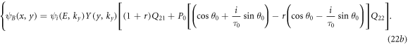
Important feature from comparing figures 2(a) and (c) is attributed to SOC including. Without SOC, the value of energy gap is almost same for K and K' valleys as 1.63 eV. SOC changes energy gap of TMDC-PSL in a few hundreds of meV, that is tunable by means of width of layers (or ribbons) and types of TMDCs.
In figure 3 energy gap pattern versus the ribbons width ratio (or hexagon number ratio, NA
:NB
is illustrated. It is clear that by taking NA
= 0 the value of energy gap is that of WSe2 and NB
= 0 gives the energy gap of MoS2. By changing the ratio of NB
and NA
the value of Eg
of superlattice is varied in both K and K' valleys, with SOC. Without SOC Eg
has same value for K and K' as mentioned and discussed in figure 2. Taking SOC into account results in considerable difference in Eg
value in both valleys. In fact, SOC removes degeneracy in the band structure of TMDC-PSL differently in K and K' valleys as it does in the case of TMDC monolayers. In order to get more insight into the effect of width ratio between neighbor ribbons or strips A, B (MoS2, WSe2) in unit cell, the value of Eg
versus NA
:NB
is shown in figure 3(d). Opposite trends can be seen for changing the value of Eg
in K and K' valleys with considering SOC, so that in the case of K valley, Eg
increases with increasing the contribution of MoS2 unit cell numbers against to that of K' valley. In order to compare with other works, we report the result of reference [47] that author's calculated a similar structure of TMDC-PSL within DFT approach. Reasonable consistency can be observed, in particular for  [NA
:NB
] = [7:3] consistency is excellent. It is worth to note that Eg is varied with the width of each ribbon because the contribution of materials (MoS2 or WSe2) is different in unit cell when we change the number of hexagons, NA and NB. Besides, SOC in each TMDC material has different magnitude. Therefore, we expect that changing the contribution of material in unit cell by changing NA and NB ratio leads to the different SOC effect in PSL.
[NA
:NB
] = [7:3] consistency is excellent. It is worth to note that Eg is varied with the width of each ribbon because the contribution of materials (MoS2 or WSe2) is different in unit cell when we change the number of hexagons, NA and NB. Besides, SOC in each TMDC material has different magnitude. Therefore, we expect that changing the contribution of material in unit cell by changing NA and NB ratio leads to the different SOC effect in PSL.
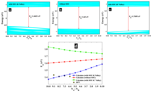
Figure 3. (a) and (b) Energy gap pattern versus number of hexagons in A and B strips in the TMDC-PSL composed of  and
and  with and without SOC effect, respectively for
  valley.
  . (c) similar to panel (a) for
  valley. (d) Energy gap versus
  Line-dotted green curve shows results of energy gap calculation for
  valley With SOC, line-dotted blue curve shows results of energy gap calculation with SOC for
  valley, line-dotted red curve shows energy gap calculation results without SOC. Yellow dotted curve shows the result from DFT calculations [47].
Download figure:
Standard image High-resolution imageFigure 4 shows 3D view and counterplot of band structure for certain energy values in energy bands of figure 2(a), recognized as A, B, C, D points in K and K' valleys.

Figure 4. (a), (b) 3D band structure of valence and conduction band of TMDC-PSL composed of  and
and  layers with the size of
  and
and  respectively for
  valley. (c), (d) Counter plot of valence and conduction bands.
Download figure:
Standard image High-resolution imageHereafter, we focus on K valley with SOC. In figures 5(a) and (b) we present band structure in ky direction for different Kx 's that is a cross section of counterplots in figure 4. Parabolic band structure in ky direction per kx (that is quantized due to spatial confinement effect in x direction) reflects free carrier behavior in y direction in which there is no confinement effects. We take unit cell length as Λ = 8zA + 2zB and Λ = 3zA + 7zB . It is clear that by varying ribbons width ratio the energy gap magnitude is increased by increasing NB . considerable shift to lower energies occurred in valence band. Also main energy gap is widened with increasing NB . It is worth to mention that unit cell length Λ is equal to wA + wB and varying wA or wB portion by changing NA or NB leads to different structure of superlattice with different ribbon widths. In order to show the energy gap variation with ky , we take into account the typical values of ky as zero and 0.5 nm−1. We found valence band red shift for higher ky . in figures 5(d), (e), 3(e), (d)) we take NA = NB = N for ky = 0.5 nm−1 and a few tens of meV increase in energy gap is observed.

Figure 5. Electronic band structure versus Ky for unit cell size of (a)  (b)
(b)  (c) Energy gap variation in
  direction versus
  for
for  (d), (e) Energy gap variation in
  direction versus
  for
for  and
and  respectively. Incident angle of electron is
Download figure:
Standard image High-resolution imageNow, we turn to consider the transmission probability in TMDC-PSL. In figure 6(a) transmission probability map versus incident electron energy and transverse wavevector (ky
) is depicted. It is clear that transmitivity is zero in energy band gap region. At allowed energy minibands transmission probability has nonzero value and in some minibands it reaches unit. Figure 6(b) illustrates the effect of λ, fraction of MoS2 nanoribbon width to whole unit cell Λ, on transmitivity. It can be seen that for bigger λ (very wide MoS2 nanoribbons) transmitivity shows oscillatory trends while for smaller λ it has smooth behavior showing that wider MoS2 nanoribbon gives rise to resonant states in particular for incoming electron energies lower that −1 eV. In the other words, oscillatory trend of transmitivity indicates quantum nature of transmission through the structure. If the MoS2 nanoribbon becomes wider, number of resonance states generated for energies lower than −1 eV is increased. Similar behavior is observed for energies higher than about 1 eV. In figure 6(e) the influence of incoming electron incident angle (see geometry in figure 1) is depicted that shows incident angle has no obvious effect on transmitivity. Figure 6(c) is plotted for  however our study implies that for other values of ky
incident angle has no effect on transmission. Figure 6(d) demonstrates incremental effect of N, (N = NA
= NB
), on oscillatory behavior of transmission at all allowed energies. It might be expected that larger number of N that subsequently increases the number of interfaces creates more maxima in transmission spectrum as it is well known in introductory quantum mechanics. Figures 6(e), (f), (d) illustrate a closer view to transmission probability. From these figures it can be understood that effective parameters of N, ky
, λ, and θ0
how enhance or weaken the transmission probability. Furthermore, it can be seen that oscillatory behavior of T that indicates the presence of resonance energies can be engineered by these parameters.
however our study implies that for other values of ky
incident angle has no effect on transmission. Figure 6(d) demonstrates incremental effect of N, (N = NA
= NB
), on oscillatory behavior of transmission at all allowed energies. It might be expected that larger number of N that subsequently increases the number of interfaces creates more maxima in transmission spectrum as it is well known in introductory quantum mechanics. Figures 6(e), (f), (d) illustrate a closer view to transmission probability. From these figures it can be understood that effective parameters of N, ky
, λ, and θ0
how enhance or weaken the transmission probability. Furthermore, it can be seen that oscillatory behavior of T that indicates the presence of resonance energies can be engineered by these parameters.

Figure 6. Counter plot of electron transmission probability versus different parameters as (a) 
 where
where  and
and  (b)
(b)  where
where  and
and  (c)
(c)  where
where  and
and  (d)
(d) 
 where
where  and
and  (e)
(e)  where
where 

 (f)
(f)  where
where 
 (g)
(g)  where
where 


Download figure:
Standard image High-resolution imageNow we illustrate the evolution of ψA
and ψB
, sublattice wavefunctions(or probability amplitude), in figure 7. We take 
 as whole system length, θ0
= 0 and also we choose three energy values: one inside band gap (second column) and two in allowed neighbor higher band (third column) and lower (first column) band. Panels in each row also depicts probability amplitudes (ψA
, ψB
) for real and imaginary parts of wavefunction in sublattices A, B with probability densities
as whole system length, θ0
= 0 and also we choose three energy values: one inside band gap (second column) and two in allowed neighbor higher band (third column) and lower (first column) band. Panels in each row also depicts probability amplitudes (ψA
, ψB
) for real and imaginary parts of wavefunction in sublattices A, B with probability densities 
 From first column in figure 7, for E = +0.825 eV in allowed band higher than band gap (reminiscent of conduction band in two-band model of a typical semiconductor) wavefunction behaves as propagating wave or Bloch wave in entire system. From dispersion relation, equation (23), for E = +0.825 eV, kx = 0.3287 nm−1 then attributed wavelength is obtained as λB
= 19.1153nm, so it is expected 8.52 periods
From first column in figure 7, for E = +0.825 eV in allowed band higher than band gap (reminiscent of conduction band in two-band model of a typical semiconductor) wavefunction behaves as propagating wave or Bloch wave in entire system. From dispersion relation, equation (23), for E = +0.825 eV, kx = 0.3287 nm−1 then attributed wavelength is obtained as λB
= 19.1153nm, so it is expected 8.52 periods  are governed by propagating wave that is confirmed by figures 7(a), (b) (determined by the number of maxima or minima). Second column indicates wavefunctions (probability amplitude) and probability density for an energy inside band gap that is decaying wave which is caused by this fact that there is no electronic state in the band. Panels g-i show mentioned parameters behavior for an energy in bands immediately lower than band gap as E = −0.648 eV that shows again a propagating wave feature similar to panels a–c.
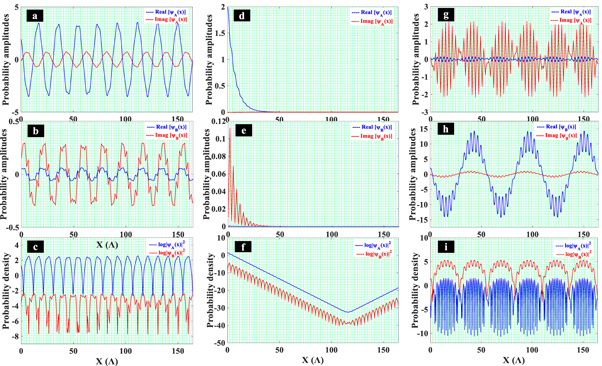
Figure 7. Evolution of probability density and amplitude for (a–c)  inside conduction band, (d–f)
  at the edge of energy gap, (g–i)
  inside valence band.
 and
and  Calculations has been performed for
  valley.
Download figure:
Standard image High-resolution imageAccording to reports on fabricating planar TMDC superlattice [3, 4], ribbons have inherent disorders in width, hence, in order to study electronic and transport properties more precisely, disorder effects are considered. To model these effects, we take whole system length as  and disorder length as three values of


 which are random numbers in three intervals of

 respectively for
  Figure 8 shows the electronic transmittivity through the structure. It is clear that main gap (around
  ) is independent of different disorders, but, higher and lower neighbor band gaps (that are determined by minima at two sides of main minimum ) are sensitive to disorder as shown in figures 8(b) and (c). Disorder effect in upper band gap is more remarkable. In figure 9 electronic transmittivity spectrum under different incident angle is depicted. It is obvious that main gap is very weakly dependent on incident angle but two other gaps experience shift with increasing incident angle. Therefore, main gap is almost independent of incident angle and disorder.

Figure 8. (a) Transmission probability for different disorders. Black curve for full periodic structure without disorder and  Blue curve for
  Green Curve for
  Red curve for

 and
and  are random numbers in the interval of
 and
and  repectively. Incident angle of electron is zero. Panels (b), (c) show the magnification of panel (a).
Download figure:
Standard image High-resolution image
Download figure:
Standard image High-resolution image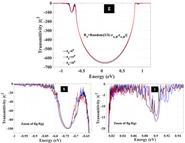
Figure 9. Transmition probability for different disorders and incident angles. (a) 

 is random number as
  (d)
(d) 

 is random number as
  (g)
(g) 
 R3 is random number as
  Panels b, c, e, h, i and f are closer view of transmitivity. Black curve: incident angle as
  blue curve:
  red curve:
 and
and  (exit angle) are zero and
Download figure:
Standard image High-resolution imageIn this part we investigate the effect of defect on transmission by considering defected ribbon in TMDC-PSL as  "D" denotes the defected ribbon, which is a wider ribbon of
  In figure 10 transmitivity for 3 different widths of defect is illustrated for incident angle
  Similar to disorder effect, it can be seen that main gap is not influenced by including defect but two aside gaps are shiftted. Also defect modes are appeared inside gaps determined by sharp peaks. In addition, shift in upper gap becomes remarkable with increasing defect ribbon width (see figures 10(b), (c)). Figure 10(d) demonstrates the behavior of all defect modes inside energy gaps by changing the width of defect ribbon from
  to
to 
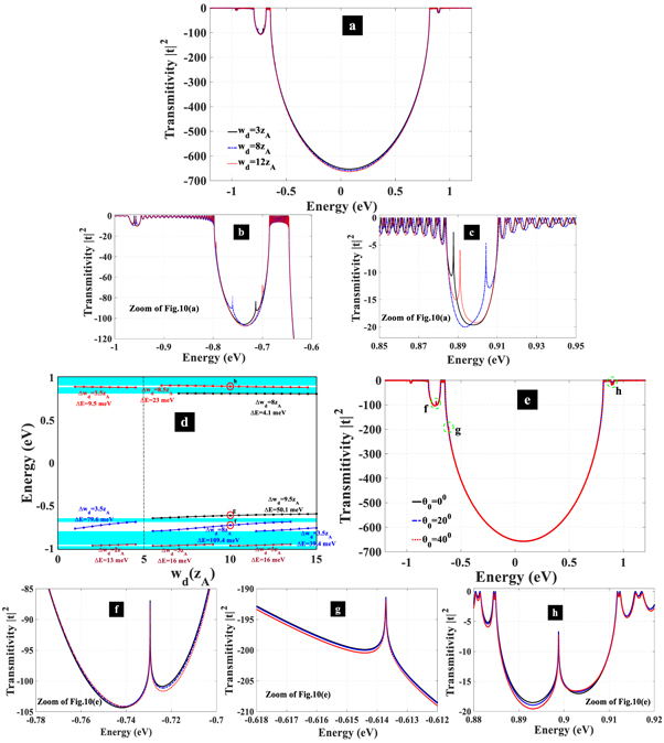
Figure 10. (a) Transmitivity of  structure with
  and
and  for three values of defect strip width. Panels b and c are closer view of transmitivity shown in panel a for energies in valence and conduction bands, respectively. (d) Defect mode trend versus defect width located inside gap. (e) transmitivity for three incident angles:
  (black curve),
  (blue dashed curve),
  (red dotted curve) with defect width of
  Panels g, f, h are magnification of panel e.
Download figure:
Standard image High-resolution imageIt is obvious that all defect modes below zero energy experience blue shift and those of higher than zero energy are red shifted. From figure, when width of defect ribbon is  that is the width of ribbon A in superlattice, defect modes disappear because system is normal
  superlattice. Figure 10(e) presents electronic transmitivity within structure under different incident angles. Obviously, for particular width of defect ribbon the location of defect modes in all energy gaps are independent of the angles, see figures 10(f), (g), (h) that show this finding in closer view.
Figure 11 illustrates the evolution of both the probability densities and amplitudes of  inside TMDC- PSL with a defect as
  at defect mode energies (points A and B in figure 11(a)). In figures 11(b), (c), (d) we take
  (energy at point A) that is −1.22 eV and incident angle
  It is clear that carrier's probability density is highly localized inside defect ribbon. To complete description of wavefunction evolution at energy
  it is interesting to see that incident wave is propagating at the entrance of structure (x = 0) and starts to decay because
  is inside the lowest gap (figure 11(a), gap A), and localize inside defect and continues decaying. Similar behavior is seen for
  (figure 11(b)). Figure 11(d) shows localization more clearly in which probability density reaches peak in defect ribbon. Figures 11(e), (f), (g) depicts similar trends for defect mode of B in the above band gap in figure 11(a), and again localization feature is pronounced in defect region.

Figure 11. Transmitivity for  structure with
  with defect width as
  Panels b, c and d show the wavefunction attributed to defect mode of A with energy value of
  Panels f, e and g show the wavefunction attributed to defect mode of B with energy value of
Download figure:
Standard image High-resolution image3.1. Conductance (σ), Fano factor (F)
Now, we consider the transmission of an electron moving inside TMDC-PSL e. g.  for different layers width ratio,
  under special incident angle of
  and we focus on Fano factor that is very important parameter in addressing shot noise and conductivity in transport properties of nanostructures. Figure 12 illustrates transmission, conductivity and Fano factor versus energy with different
  for finite periodic structure. Varying
  has considerable effect on transmission probability that is depicted in figure 12(a). Two typical values of
  have been considered that change the transmission probability spectrum by shifting it. The amount of shift is much more pronounced for lower subband (lower than main gap). Similar trend can be seen in conductivity spectrum, see figure 12(b). As it is expected, conductivity reaches zero in gap region for both values of
  again shift of conductivity spectrum is more considerable in energies below zero. Corresponding Fano factor in the band gap tends to integer 1, figure 12(c). The effect of changing
  has still significant effect on lower subband energies. Outside the band gap, as the energy increases (absolute value) conductivity increases linearly with oscillations caused by propagating modes in finite structure. Also we notice that the Fano factor changes from 1 to smaller values gradually, indicating that transport becomes ballistic. In order to get deeper insight, figures 12(d), (e), (f) depict transmitivity, conductivity and Fano factor versus
  and certain values of energies in upper and lower subbands. Apparently for pure
  (B ribbon) that is
  conductivity exhibits a factor of minimum
  at energies higher and lower than gap region. Furthermore, for
  Fano factor has minimum value for these energies, even below

Figure 12. Panels a, b, c are spectrum of transmitivity, conductivity and Fano factor, respectively for  (blue curve) and
  (black curve) with
  Panels d, e and f show the behavior of transmitivity, conductivity and Fano factor with changing
  for different energies. Colors correspond to energy positions in panel b, c which are determined by dashed circles.
Download figure:
Standard image High-resolution imageIn figure 13 the effect of incident angle is investigated. To give an overview in figures 13(a), (b), (c), transmission probability, conductivity and Fano factor spectrum for two typical values of incident angle, are shown. The main gap and other lower gaps are independent from incident angle and transmitivity variation with changing incident angle is not remarkable. From figures 13(b), (c), incident angle doesn't shift the conductivity and Fano factor spectrum but changes their values outside gap region. Furthermore, in figure 13(c) at energy around −1.25 eV Fano factor is above  for
for  and less than
  for
for  showing that Fano factor can be adjusted by incident angle. In figures 13(d), (e), (f) for particular energies of lower and upper subbands (than main bandgap), incident angle is swept. Interestingly, it is found that incident angle has no considerable impact on transmission probability but changes conductivity and Fano factor more remarkably, which has decremental and incremental effect, respectively, for all values of energies (not shown here).

Figure 13. Panels a, b, c: transmitivity, conductivity and Fano factor spectrum, respectively for  (blue curve),
  (black curve).
  Panels d, e, f: transmitivity, conductivity and Fano factor versus incident angles for different energies. Colors correspond to energy positions in panel b, c which are determined by dashed circles.
Download figure:
Standard image High-resolution imageFinally, we turn our attention to the effect of unit cell size,  on transport properties of TMDC-PSL. As it was mentioned before, increasing unit cell size results in narrowing main bandgap. Hence, from figure 14(a), it is obvious that transmitivity and main energy gap are varied remarkably . Similarly, considerable effects can be seen in conductivity and Fano factor spectrum. By decreasing unit cell size, conductivity is weakened, and subsequently Fano factor is enhanced. Also, decreasing unit cell leads to shifting conductivity and Fano factor spectrum and increasing the number of picks due to enhancing propagation modes of superlattice. In figures 14(d), (e), (f), the effect of varying unit cell size has been considered to show its overall effect, for typical energies in upper and lower energy subbands. Opposite behavior of conductivity and Fano factor is still seen.

Figure 14. Panels a, b, c are transmitivity, conductivity and Fano factor, respectively for  (blue curve) and
  (black curve).
  Panels d, e and f are transmitivity, conductivity and Fano factor, respectively versus
  (
( ).
).
Download figure:
Standard image High-resolution image
4. Conclusion and remarks
We found that without spin orbit coupling, the value of energy gap is almost same for  and
and  valleys . SOC changes energy gap of TMDC-PSL in a few hundreds of meV, that is tunable by the width of ribbons and kind of materials. Furthermore, SOC removes degeneracy in the band structure of TMDC-PSL and shifts valence bands differently in k and k' valleys. Opposite trends were seen for behavior of
  in
in  and
and  valleys with considering SOC. For
  valley,
  increases with increasing the portion of
  in unit cell against to that occurred in
  valley. Also, valence band experiences red shift for higher value of
  It is also shown that for bigger
  (wide
(wide  nanoribbons) transmitivity shows oscillatory trends while for smaller
  it has smooth behavior showing that wider
  nanoribbon gives rise to resonant states. Parameters

 and
and  enhance or weaken the transmission probability. We further found that main gap is almost independent of incident angle and disorder and two neighbor gaps experience shift with defect modes that are appeared inside these gaps. Finally, we have seen that for pure MoS2 (
 ) conductivity exhibits a factor of minimum
  at energies higher and lower than gap region. Furthermore, for
  Fano factor has minimum value for these energies, even below
  Fano factor above
  is seen for certain value of energies and incident angle. Decreasing unit cell (number of hexagones) leads to conductivity and Fano factor spectrum shift with increasing the number of peaks due to enhancing propagation modes of superlattice. While our theoretical study is simple compared to DFT approaches, presents an efficient way to control the key parameters effects on conductivity and band structure of TMDC-PSL and paves a way towards pertinent experiments.
Data availability statement
The data generated and/or analysed during the current study are not publicly available for legal/ethical reasons but are available from the corresponding author on reasonable request.