


Abstract
A drop in the efficiency of light-emitting diodes based on InGaN/GaN QWs known as the 'green gap' has been studied intensively over the past dozen years. Several factors were revealed to contribute to its origin, such as random fluctuations in the indium concentration or the diffusion of point defects during the growth of QWs. The aim of this paper is to demonstrate that the Kirkendall effect can be the mechanism responsible for the thermal decomposition of InGaN/GaN MQWs structures, contributing to the green gap problem. By applying density functional theory, harmonic approximation, and harmonic transition state theory, we calculated the heights of the migration energy barriers of In and Ga atoms diffusing in  alloys (
 ), the vibrational frequencies of
  alloys in the presence of migrating point defects, the temperature dependencies of the defect migration energy barriers and diffusion coefficients of Ga and In atoms migrating in
  alloys. We demonstrated the presence of unbalanced diffusion rates of In and Ga atoms at the
  interfaces and finally explained the experimentally observed mechanism of void formation at the
  interfaces by means of the Kirkendall effect.
Export citation and abstract BibTeX RIS

Original content from this work may be used under the terms of the Creative Commons Attribution 4.0 license. Any further distribution of this work must maintain attribution to the author(s) and the title of the work, journal citation and DOI.
1. Introduction
During the past two decades, (In,Ga)N-based optoelectronic devices emitting in the blue and green wavelength regions have been intensively investigated. In particular, InGaN/GaN quantum wells (QWs) applied in light emitting diodes and laser diodes are of special interest. This is due to their wide applications in lighting, communication, displays, medicine, and the environment. It is well known that the structural quality of the active regions  , that is, the compositional homogeneity of multiple QWs (MQWs), as well as their interfacial morphology, have a significant impact on device performance [1–7]. The fabrication of In-rich (
 ) InGaN QWs with high material quality remains the most challenging. This is due to two main factors. One is the high compressive strain caused by the large lattice mismatch between
  and GaN, and the other is the low thermal stability of the In-rich InGaN QWs. The presence of a high defect density in the
  layers can be induced by three main factors: In-content fluctuations [8], high concentration of point defects [9], and misfit dislocations observed in layers above their critical thickness [10]. As reported by several authors, In-rich InGaN QWs tend to degrade during the growth of p-type capping layers, which reduces the optical properties of the InGaN QW active region. This phenomenon has been observed both in single and multi-QW structures
  [2–7, 11–14].
In particular, Queren et al investigated the thermal stability of InGaN thin layers [3]. On the basis of photoluminescence, electroluminescence, and SIMS measurements, they showed the effect of thermal degradation of the laser structure composed of an InGaN single QW surrounded by barriers with various composition; GaN, InGaN, or AlGaN. This process was observed during annealing (at temperatures greater than or less than  C) and was accompanied by the diffusion of In atoms, which took place both in the lateral and vertical directions of the structure. Next, Thaler et al [4] investigated the thermal stability of
  thin films on GaN with x = 0.08–0.18 in the thermal annealing process, as a function of indium concentration, temperature and time. They showed that InGaN layers with a higher indium concentration decomposed faster at a given temperature compared to those with a lower In concentration. On the basis of the dependence of the photoluminescence intensity vs. temperature, they came to the conclusion that point defects were generated during annealing prior to the onset of InGaN/GaN QW decomposition. The authors demonstrated that for the layers with the higher indium concentration, the decomposition proceeded via the formation of metallic indium and gallium precipitates within the InGaN layer. Similar In-rich precipitates with sizes much larger than the original InGaN QW thickness were observed by Li et al in the studies on the local decomposition of the InGaN QW during the growth of the p-type layer, caused by temperature [5]. The formation of metallic clusters was also explained by the diffusion of In atoms, which led to a reduction of the indium content in the surrounding InGaN layer. The formation of nonradiative defects containing voids was also observed in semipolar
  ,
,  oriented InGaN/GaN QWs [6, 7]. As reported, the average size of these defects (50–100 nm) and the density up to
  strongly depended on the post-QW growth annealing time and temperature, while their growth was initiated in the InGaN/GaN active region.
Analogous degradation processes were also experimentally observed in the case of  MQWs structures. Already in 1999 Romano et al [11] demonstrated phase separation in structures of
  MQWs after annealing at 975
  C. Transmission electron microscopy (TEM) images revealed In-rich precipitates and voids, often found in pairs, only within the QW region. Their formation was initiated at dislocations and InGaN/GaN heterointerfaces. The observed phase separation in the presence of voids was explained by preferential segregation of In atoms to the void, as a way to relieve the large compressive strain in the InGaN films. Additionally, based on the optical transition spectrum of the
  MQWs system annealed at atmospheric pressure, the Authors suggested also the presence of gallium vacancies in the InGaN QW area. Next, Daele et al [12] investigated the formation of metallic In regions in the InGaN/GaN MQWs system that was the result of either capping the active region with a p-type GaN layer or thermal annealing. The authors reported on the transformation of the whole InGaN QW area into metallic In platelets with a diameter between 50–100 nm and a height slightly larger than the initial QW thickness, embedded into an In-poor GaN matrix. It was demonstrated that the process of decomposition of InGaN QW into GaN and metallic In platelets was thermally activated; furthermore, the presence of dislocations in the system pointed to a diffusion of In and Ga atoms. A similar observation regarding the decomposition of the active InGaN/InGaN double QW active region in the blue laser diode structure was made by Hoffman et al [2]. Decomposition occurred after deposition of a p-type GaN capping layer at 950
  C and resulted in the formation of In-rich platelets adjacent to the voids, identified by SEM and HRTEM techniques. As reported, the decomposition process was initiated by phase separation into Ga- and In-rich regions inside the InGaN active region. Analogously, the presence of multifaceted voids caused by the aggregation of gallium vacancies and induced by the diffusion of In/Ga atoms was observed in a double heterostructure
  with a porous InGaN layer, leading to the degradation of the QW InGaN [15].
Recently, our group has studied the impact of metal vacancies present in GaN layers on the thermal decomposition of the  QW system [13, 14]. The structures analyzed were grown using MOVPE on GaN n-type substrates (either not implanted or implanted with He ions), and the samples were annealed at three different temperatures (900
  C, 920
  C and 940
  C) [13]. By using photoluminescence, HRXRD and STEM techniques, we showed a significant decomposition of InGaN QWs, which started in samples grown on implanted GaN substrates at lower temperatures than in samples grown on unimplanted ones, that is, at 920
  C. Similarly to the previous results, within the degraded QWs, we demonstrated the presence of metallic In precipitates and voids. We concluded that gallium or indium vacancies were responsible for the degradation of QWs, diffusing from the GaN substrate to the area of InGaN QWs, whose diffusion rate should be significant, since it took place at least at a distance equal to the thickness of the GaN substrate, i.e. 56.5 nm. Next, in [14] we investigated different stages of degradation of
  MWQs with various compositions (
 ), as well as their transformation into voids that expanded during annealing (at 900 ∘C–950
  C). We showed that the initial stage of the formation of the void was due to the clustering of metal vacancies. Small initial voids were present near the completely degraded regions of the
  QWs, where larger final voids, partially filled with indium precipitates and amorphous material, could also be observed. In particular, we showed that for a QW with the composition
  , the indium atoms identified in the final void had to diffuse a distance equal to 150 nm from the region of the QW.
As follows from the presented review of experimental papers, a common thread appearing in the description of degradation of the  QW system is the diffusion of atoms (In or Ga) and the formation of voids. These processes are temperature-induced (annealing or growing a capping layer). Therefore, it may be assumed that the Kirkendall effect can be the cause of the degradation of the InGaN/GaN QW system. In this classical phenomenon, initially observed in bulk metals [16, 17], the key is the nonequilibrium process of vacancy mediated diffusion of atoms through the interface of two materials, taking place at elevated temperatures. As a consequence of the unbalanced diffusion rates between the two stacked metals, vacancies are injected at the interface region within the faster diffusing metal. The coalescence of excess vacancies leads to the formation of voids distributed along the interface, during the whole annealing process. Historically, this effect provided the first evidence that vacancy-mediated hopping of atoms was the predominant mechanism for diffusion in crystalline materials [16–18]. It should also be taken into account that in 2004, Yin et al [19] revealed the Kirkendall effect at the nanoscale and showed that it is an extremely useful 'tool' for engineering and designing hollow nanomaterials. Since this discovery, the Kirkendall effect has been considered a very effective strategy for the synthesis of hollow nanostructures such as hollow nanospheres and nanotubes [20], modified nanoparticles [21], or nanocrystals [18].
The aim of this paper is to show that the Kirkendall effect is the mechanism responsible for the thermal decomposition of the InGaN/GaN MQWs system. Since at its foundations lies the motion of the atoms, which is a consequence of the difference in their diffusion rates within each material, it is necessary to find the unknown diffusion coefficients  of metal atoms in the
  systems with various compositions. This will be the main task of this paper. For this purpose we will use the first-principle calculation in the framework of Kohn–Sham density functional theory (DFT). The paper is organized as follows. Section 2 presents the methodology used to calculate the diffusion coefficients
  and
and  of indium and gallium atoms, within the framework of harmonic transition state theory (HTST). In section 3.1 the heights of the migration energy barriers of the Ga and In atoms in the alloys
  with different compositions (
 ) are calculated, together with the vibration frequencies of the alloys
  in the presence of defects (section 3.2), as well as the values of the diffusion coefficients
  and
and  in these alloys (section 3.3). Section 3.4 provides the discussion on the Kirkendall effect applied to the description of the thermal decomposition of the
  MQWs system. Finally, we conclude the results obtained.
2. Theoretical approach and computational details
2.1. Calculation method and model
Our calculations were performed in the framework of Kohn–Sham DFT by means of SIESTA program [22, 23]. The exchange-correlation interaction was described by the general gradient approximation, and we used a version of the Perdew–Burke–Ernzerholf potential with parameters β, µ and κ fixed by the jellium surface (Js), jellium response (Jr), and Lieb–Oxford bound criteria, respectively [24, 25]. The electron–ion core interactions were represented by Troullier–Martins type pseudopotentials and the electron wavefunctions were expanded into the atomic orbital basis set using either single-ζ, triple-ζ, or triple-ζ polarized (N:  ,
,  ; Ga:
; Ga:  ,
,  ,
,  ; In:
; In:  ,
,  ,
,  ,
,  ). The cutoff energy of 500 Ry was used to produce a real-space mesh, and Brillouin zone sampling was carried out using a
  Monkhorst–Pack k-point grid for a primitive unit cell of bulk GaN. The positions of all atoms in the GaN unit cell were relaxed with the convergence criteria imposed on the atomic forces being less than 0.001 eV Å−1. This geometry optimization led to the following lattice constants for bulk GaN:
  Å and c = 5.220 Å. They can be compared with the experimental data obtained by x-ray diffraction
  Å and c = 5.185 Å [26].
An alloy  (x = 0.11 and x = 0.22) was represented by means of a supercell model of size
  . Inside each GaN metal layer, a certain number of In dopant atoms were randomly placed at the lattice sites to reflect the compositions most similar to the cases of
  and
and  . The geometric model of the supercell with 108 atoms is shown in figure 1. All atomic positions of this alloy were optimized again with the force restriction imposed to be less than 0.002 eV Å−1. The prepared supercells were used to calculate the heights of the migration energy barriers of Ga and In vacancies along the hexagonal c axis by means of the nudged elastic band method [27–29].

Figure 1. (a) A supercell model of  alloy with
  Å,
Å,  Å. (b) A scheme presenting the initial, transition, and final states of the atomic diffusion.
Download figure:
Standard image High-resolution image2.2. Lattice dynamics
To investigate the thermal properties of the discussed system, such as the temperature dependence of the diffusion coefficients of In and Ga atoms, we performed phononic calculations using a direct method in harmonic approximation. This means that phonon frequencies are considered volume independent, and the thermal expansion coefficient is equal to zero at all temperatures [30]. For phononic calculations, a larger supercell was built by multiplying the structure presented in figure 1 by a factor  , which led to a system
  of 963 atoms. This larger system was used to calculate force constant matrices by means of the finite-displacement method. Only the Γ point sampling was used at this stage of the calculations. A displacement of 0.03 Bohr (0.016 Å) was applied in each direction
  for every atom in a centrally located cell. In the harmonic approximation, the obtained force constant matrix is transformed into the dynamical matrix D, and the vibration frequencies of the atoms are determined by solving an eigenvalue problem of the matrix D [30–32].
Based on the vibrational spectra, several properties, such as the zero-point vibrational energy  , as well as the vibrational energy
  , the vibrational entropy
  and the free energy
  can be determined as functions of temperature T [33]:
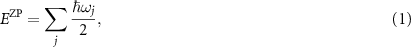


where  , kB
, and ωj
are the reduced Planck constant, the Boltzmann constant, and the angular frequency of each jth mode of vibration, respectively. In order to apply equations (1)–(4) for crystals, it is necessary to include a frequency dependence on the wave vector, that is,
, kB
, and ωj
are the reduced Planck constant, the Boltzmann constant, and the angular frequency of each jth mode of vibration, respectively. In order to apply equations (1)–(4) for crystals, it is necessary to include a frequency dependence on the wave vector, that is,  . Thus, integration over the first Brillouin zone or summation over special k-points must be performed [34, 35]. In this study, the sampling of the k-space was tested and finally carried out on a grid of
  , which is equivalent to 64 points.
2.3. Diffusion coefficient theory
Usually, the temperature dependence of the diffusion coefficient D is consistent with the Arrhenius formula [36]:

where  is the activation enthalpy of diffusion and D0 denotes the pre-exponential factor also called the frequency factor. This is an empirical relationship according to which the diffusion coefficient is described at the macroscopic level by fitting to the experimental results.
At the atomic level description, the diffusion coefficient D is usually written in the following form:

This means that D is proportional to the jump rate constant Γ and the distance l that the atom moves to a neighboring site, multiplied by any correlation factor f that includes the number of possible jump sites in a given lattice type and diffusion dimension. For a hexagonal closed packed hcp lattice, the factor f equals 0.781 [37]. In the case of the vacancy mediated mechanism, the probability that a neighboring location could accept a particle should also be taken into account, so the vacancy concentration cV
should be included as the scaling factor of the coefficient  . Vacancy concentration is defined as the ratio between empty lattice sites and all lattice sites in a system. It is calculated according to the expression:

where  is the Gibbs energy required to create a vacancy. In general, the formation energy depends on the Fermi level position and the charge state of the defect. Because our goal is to compare the mobility of the gallium and indium atoms in the same material at any vacancy concentration, we will focus our efforts on determining the part related to the barriers to atomic hopping. Therefore, in the following considerations, we shall not discuss the vacancy formation energy and vacancy concentrations.
Individual jumps of atoms are promoted by thermal activation and can be described by the Eyring equation derived from the transition state theory [38]:

where the prefactor  is a universal frequency and
  is the difference in the Gibbs free energy between the barrier saddle point and the equilibrium position. According to thermodynamic rules, it can be separated into enthalpy and entropy terms:
  . Equation (8) has been shown to be consistent with the simplified Vineyard formula [39, 40]:
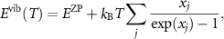
where νi and νj are the vibration frequencies in the initial and transition states and N is the total number of frequencies. By comparing expressions (6) and (8) with (5), the prefactor D0 can be written as the part depending on the change in entropy during the migration of the atom in the system. The entropy of diffusion corresponds to the change in lattice vibrations associated with the displacement of the atom from its equilibrium to the saddle point configuration.
Using DFT calculations, it is possible to determine the changes in the total energy of the system ( ) between the transition state and the equilibrium point, that is, the energy barrier (
 ) for atom migration. Additionally, phonon calculations make it possible to determine the frequencies of vibrations of atoms and, on their basis, to determine the vibrational free energy (
 ) as a function of temperature. To simplify the calculations, pressure-induced effects in the crystal are neglected, and only a constant-volume system is considered here. Thus, an approximation of the Gibbs energy changes by the Helmholtz free energy can be used:

Thus, the jump rate equation based on the data from the DFT calculations will be as follows:

Dependence (11) is consistent with the Eyring and Vineyard equations.
3. Results and discussion
3.1. In and Ga atom migration in  via the vacancy mediated mechanism

In order to calculate the diffusion coefficients of Ga and In atoms in  alloys, it is necessary to find the heights of the migration energy barriers of the corresponding point defects (see equations (6) and (11)). We assumed the diffusion of Ga and In atoms took place in the c direction of the hexagonal supercell, via the vacancy mediated mechanism, see figure 1.
The first assumption is based on the fact that the experimental papers discussed in the Introduction [2–5, 11–15] concern single- or multi-QW InGaN/GaN systems, grown just along the hexagonal c direction, and that the thermal decomposition of the InGaN/GaN QWs system occurred also in this direction. The thermal decomposition of the InGaN/GaN MQW system observed by us [13, 14] starts from the first QW, and later, with the increase in temperature and time, the next QW in the c direction is decomposed, up to the last one (see figure 12 [13]). Therefore, the direction c is crucial from the experimental point of view. The second assumption concerns the choice of the diffusion mechanism. It is known that the vacancy mediated diffusion mechanism is based on a usual jump between an empty lattice site and the site occupied by an atom, and that this mechanism is of particular importance in the situation when atoms migrate within the same sublattice, e.g. metal atoms having a similar ionic radius (In or Ga) in the metal sublattice. This mechanism is very important [41–43] in nitrides. It also follows from the experiment that in the case of thermal decomposition of the  QWs, there is a high concentration of vacancies in the structure [2–5, 11–15]. Moreover, as was mentioned in the Introduction, the Kirkendall effect, which we propose as the mechanism responsible for the thermal decomposition of the
  QWs, is based just on this mechanism. Therefore, we chose the vacancy mediated diffusion mechanism as the main one to be explored herein.
The calculated heights (by means of the nudged elastic band method) of the migration energy barriers  of vacancies
  and
and  in
in  alloys with various compositions (
 ) are presented in table 1.
Table 1. Heights of the migration energy barriers of vacancies  and
and  in alloys
  .
.
| % of In in | Energy barrier  , eV , eV | |||
|---|---|---|---|---|

|

| |||

| This paper | Others | This paper | Others |
| 0 | 2.81 | 2.75, 2.8 [42, 44] | 2.10 | 2.10 [44] |
| 0.11 | 2.78 | 2.01 | ||
| 0.22 | 2.69 | 1.37 | ||
As can be seen in table 1, the height of the energy barrier of  in bulk GaN is in good agreement with the calculations presented in other papers [42, 44]. With the increase in the concentration of In atoms in alloys of
  up to 11% and 22%, the heights of the migration energy barriers of
  decrease slightly. Figure 2 presents a comparison of the energy barriers profiles of the Ga and In atoms migrating in alloys
  . When the concentration of In atoms is equal to 11%, the energy barriers related both to the migration of Ga and In atoms are lowered insignificantly. However, in the case of x = 0.22 an essential decrease in the height of the energy barrier of the migrating In atom is observed (see figure 2(b)). This indicates a possible greater diffusion of In atoms compared to Ga atoms in alloys
  . It follows from the shape of the energy barriers presented in figures 2(a) and (b) that the local environment of the migrating Ga and In atoms has no significant influence on the initial and final state of the diffusion process, even at higher dopant concentrations. It can be proven by the fact that the position of the base and the bottom of barrier on the energy scale corresponds to the value of 0 eV, in most analyzed cases. It means that when the migrating Ga or In atom starts the diffusion from the lattice site (lattice node) corresponding to the initial state of the diffusion, it finishes it also in the lattice site (lattice node), corresponding to the final state of the diffusion. Only for the Ga atom migrating in the
  alloy we can observe a small influence of the local environment on the final state of the diffusion of this atom. This migrating Ga atom after overcoming the energy barrier of 2.69 eV in the saddle point (transition state) returns not to the lattice site located to the lattice node, but in its neighborhood.

Figure 2. Profiles of the migration energy barriers of (a) Ga and (b) In atoms in  systems.
Download figure:
Standard image High-resolution imageThe decrease in the energy barrier that is observed with the increase in indium concentration in the  systems can be easily explained by the geometry relaxation of the system. As is known, the lattice constant of GaN
 ![$a \mathrm{[GaN]} = 3.190$](https://content.cld.iop.org/journals/1367-2630/24/12/123007/revision2/njpaca698ieqn106.gif) Å which is smaller than that of a[InN] = 3.545 Å. The
Å which is smaller than that of a[InN] = 3.545 Å. The  structure is therefore strained. A manifestation of internal strain is the value of pressure inside the relaxed system. Our numerical calculations show that in the case of the relaxed
  system, the internal pressure is 76.3 kbar, while in the case of
  this pressure increases to the value of 163.9 kbar. The introduction of the single-point defect
  or
or  into the
  system and its relaxation leads to a decrease in pressure by about 17 kbar, while the introduction of an analogous single point defect into the
  system and its relaxation results in a double decrease in pressure, i.e. by about 36 kbar. This situation occurs when defect
  or
or  is introduced into the lattice node (initial or final states). When an In atom migrates in a defected
  system and reaches the saddle point (transition state), then the decrease in pressure of the relaxed system reaches 21 kbar, but when an In atom migrates in the analogous
  system and reaches the transition state, then the decrease in pressure is down to 44 kbar. This is, in our opinion, the main physical reason for the decrease in the migration energy barrier observed with the increase in the indium concentration in the
  systems.
Additional, essential information about the possibility of diffusion of gallium and indium atoms can be provided by the temperature dependence of  , which will be analyzed in the next section.
3.2. Phonon dispersion relations
Next, we computed the phonon spectra of  systems in the presence of migrating Ga or In atoms in the crystal lattice between the initial, transition (saddle point) and final sites, via the vacancy mediated mechanism. To verify the phonon calculations of the
  systems, we calculated the phonon spectrum of a bulk GaN crystal which is presented in figure 3. As can be seen, there is good agreement between the data obtained and other theoretical and experimental results [33, 45].

Figure 3. Phonon dispersion relations calculated for bulk GaN.
Download figure:
Standard image High-resolution imagePoint defects such as vacancies or substitutional atoms present in the crystal lattice make a shift in the frequency of vibrational modes of the phonon spectrum in comparison to the spectrum of an ideal bulk crystal. This is related to a local change in the forces that act between the atoms. Figure 4 presents the phonon spectra of the system  , where a migration of Ga and In atoms occurred between the initial and final lattice sites, throughout the saddle point (transition state). As can be found from figures 4(b) and (d) a single negative mode appears in the vibrational spectrum of the system only when the migrating atom is in the saddle point (transition state). The spectra presented in figure 4 corroborate both the appropriate convergence parameters and the supercell size chosen for the calculation [40, 46]. The frequencies of these negative modes of the systems studied were further eliminated in calculations of the jump rates Γ of the Ga and In atoms, according to equation (11) [40].

Figure 4. Phonon dispersions relations of  with the migrating atoms: Ga in (a) initial state, (b) transition state (saddle point) and In in (c) initial state, (d) transition state (saddle point).
Download figure:
Standard image High-resolution imageNext, we tested various densities of k-point grids necessary to calculate the vibrational free energy and diffusion coefficient, using the standard procedure, presented in [40]. The tests were carried out on grids of points  ,
,  ,
,  ,
,  and
and  . Figure 5 presents a temperature dependence of the vibrational free energy difference
  of the Ga atom that migrates between the transition and initial states in GaN's supercell, taking into account the zero-point vibrational energy difference
  (see equation (4)). As can be traced in figure 5, the choice of k point density does not influence only the zero-point vibrational energy difference; however, it is essential at higher temperatures [40], starting from 300 K. Note also that the differences in the values of vibrational free energy
  calculated for the
  ,
,  , and
, and  -point grids almost coincide for temperatures higher than 300 K. The optimal density of the k-point grid to calculate the vibrational free energy of the
  system is therefore, in our opinion,
  , which corresponds to 64 k points.

Figure 5. Changes in the vibrational free energy (including zero-point vibrations) versus temperature for the migration of Ga atom in bulk GaN's supercell at various k-point grid density.  is the vibrational free energy difference of migrating Ga atom between the transition and initial states in GaN's supercell.
Download figure:
Standard image High-resolution imageAs mentioned in section 3.1, essential information on the possibility of diffusion of Ga and In atoms in  alloys can be provided by the shape of the temperature dependence of the migration energy barrier
  (see equation (10)). For the selected grid of
  points, we calculated
  of Ga and In atoms in
  alloys that are presented in figure 6. As can be seen, the behavior of both barriers is similar to that observed in T = 0 K, that is,
  , and their heights are essentially decreased with increasing concentration of In atoms (compare figure 2). Moreover, each barrier decreases with temperature; however, the functions
  exhibit different slopes for particular In atom concentrations in
  . For the temperature T = 1200 K corresponding to the decomposition of QWs in alloys
  [13, 14], the
  of In is equal to 0.87 eV in
  . As follows from table 1, the initial value of this barrier was 1.37 eV in T = 0 K. In the case of the Ga atom that migrates in this alloy,
  eV, which means that the initial energy barrier decreased only by 0.43 eV. Therefore, we can state that the increase in the temperature in the system affects the diffusion of In atoms in the alloys
  .
.

Figure 6. Temperature dependencies of the energy barriers  of Ga and In atoms in
  alloys.
Download figure:
Standard image High-resolution image3.3. Diffusion coefficients of indium and gallium atoms in

As mentioned in the Introduction, the phenomenon of thermal decomposition of  QWs has been intensively investigated over the past years [2–5, 11–15]. The last experimental results of our group show that the diffusion of point defects is a dominant factor that contributes to this process [13, 14, 47].
In order to fully explain the mechanism responsible for the decomposition process, it is necessary to take into account both the heights of the migration energy barriers of particular point defects and the diffusion coefficients of atoms migrating in the crystal lattices of InGaN and GaN. Recent theoretical calculation results show that the heights of the migration energy barriers of In and Ga atoms in bulk GaN are almost twice smaller than those of N atoms;  , see table 1 and [42, 44]. Furthermore, Harafuji [48] et al using molecular dynamics simulations showed that the self-diffusion coefficient of Ga atoms in bulk GaN was
  and
and  at 1500 K and 2000 K, respectively, while the self-diffusion coefficient of N atoms was less than
  at 2000 K. This means that a nitrogen vacancy is less mobile and plays the role of a base for Ga movement through the generation and disappearance of Ga–N–associated vacancies [48]. The last statement was also confirmed by Ambacher et al [49]. They measured the self-diffusion coefficient of nitrogen versus temperature in the temperature range 770
  C–970
C–970  C in a hexagonal GaN crystal, based on the results of concentration depth profiles determined from SIMS signals. Their results show that the nitrogen self-diffusion coefficient at 800 ∘C and 900
  C was
C was  and
and  [49]. The high stability of the nitrogen sublattice of GaN was also confirmed by Sadovyi et al by determining the low values of the oxygen diffusion coefficients
  and
and  at 2775 K and 3375 K, respectively [50].
Based on equations (6) and (11) we calculated the diffusion coefficients of the Ga and In atoms,  and
and  , in alloys
  with various compositions. The temperature dependencies of
  and
and  are presented in figure 7. As can be observed, an In atom is more mobile in the
  alloy than in bulk GaN, while the Ga atom is slightly more mobile in bulk GaN than in alloys
  (
( ). Moreover, indium atoms diffuse faster than gallium atoms both in
  alloys and in GaN. It follows from our calculations that the diffusion coefficient
  of indium atoms in
  is by four orders higher than that of Ga atoms in GaN. For example, at 1200 K,
  ,
,  ,
,  , and
, and 
 . This means that at the annealing temperature
  C of
C of  MQWs system [13] approximated value of the indium atom diffusion coefficient,
  , is of the order of
  , and that of the Ga atom,
  , in the GaN barrier area is
  . The results obtained above agree well with the data reported by Harafuji et al [48] for GaN.

Figure 7. Calculated diffusion coefficients for Ga and In atoms in  alloys.
Download figure:
Standard image High-resolution image3.4. Kirkendall effect as the mechanism of thermal decomposition of QWs
Based on the results presented in section 3.3, the corresponding diffusion fluxes of metal atoms between the GaN barrier area and the InGaN QW can be presented schematically in figure 8(upper panel). During the annealing of two stacked materials, GaN and  , at a temperature high enough to thermally activate the diffusion of the atoms, the migration of the atoms can occur at the interface of these materials, where the atoms will diffuse from
  to GaN and vice versa. Since the In atom diffuses into InGaN much faster than the Ga atom in GaN, the flux density of the In atoms that migrate from
  to GaN (
 ) will be much higher than the flux density of the Ga atoms that diffuse in the opposite direction (
 ). As a result of such an annealing process, a layer of
  alloy is formed with a higher In content, compared to the initial In concentration in the
  QW, located between the two sides of the phase boundary. The final thickness of this
  layer depends on both the temperature and the annealing time. It is important that as a consequence of the unbalanced diffusion rates of atoms between the
  and GaN materials, vacancies will be introduced into the interfacial area within
  , whose flux density in figure 8 is denoted
  . Therefore, the alloy region with a high In content will be more extended within the GaN barrier region, and vacancies will be introduced in the interface region in the
  QW.
QW.

Figure 8. Schematic illustration of a nonequilibrium lattice diffusion at the InGaN/GaN interface by the Kirkendall effect ( ,
,  , and
, and  are the diffusion fluxes of indium, gallium, and metal vacancies, respectively).
Download figure:
Standard image High-resolution image
Over time, the coalescence of excess vacancies will lead to the formation of small voids spread throughout the entire  well area. This process is presented schematically in figure 8(lower panel). It should also be noted that in the system discussed, diffusion of nitrogen vacancies may also occur, which is observed experimentally at the InGaN/GaN interfaces [51–53]. However, due to the experimental values mentioned above of the diffusion coefficient of nitrogen atoms (
 ), it should be assumed that the flux of diffusing nitrogen vacancies in the analyzed system will be a minority one. Although the experimental value of
  in
in  (
( ) is not known, it should not be significantly different from the known value for GaN, due to the relatively small concentration of In atoms in the alloy
  considered. Therefore, in our opinion, the described and illustrated process can be adequately explained by the well-known Kirkendall mechanism, which is already used to describe the processes taking place at the nanoscale. The values of the diffusion coefficients
  and
and  calculated by us indicate that the main reason for the thermal decomposition of the
  QW system is the diffusion of In atoms. As we showed in our paper [14], the temperature-induced decomposition of the
  QW system is a process of several stages, initiated by the formation of 'initial voids', which eventually take the form of 'final voids' with areas where metallic indium precipitates and InGaN amorphous material can be identified (compare figures 3–5 in [14]). The In precipitate areas originate from the diffusion of In atoms that occurs through the dominant flux
  . Therefore, in our opinion, the described Kirkendall mechanism is the process responsible for the 'initial voids' stage of formation. Based on the calculated temperature dependencies of the diffusion coefficients
  and
and  , one can estimate the diffusion lengths L of both metal atoms in the alloy
  at two experimental annealing temperatures applied in [14], i.e.
  C and
C and  C. Using the relation
  where t is the annealing time equal to 30 min. [14], we calculated the following diffusion length ratio
  already for the lowest
  C annealing temperature (
 at
at  C). This means that indium atoms can diffuse in the
  QWs system distances, which are by at least one order of magnitude longer than those of gallium atoms.
Moreover, the preferred diffusion direction of In atoms should be the direction toward the GaN substrate. This is due to two reasons: first, the GaN substrate is a much bigger reservoir of metal vacancies than the area of the GaN barrier and second, there is only one interface towards the GaN substrate, as opposed to their whole set, corresponding to the five InGaN/GaN QWs. As was shown in [44] there is an embedded internal electric field present at the InN/GaN interface area that influences the motion of the vacancies; moreover, the preferred migration direction of the In atoms, conditioned by the presence of a lower migration energy barrier of  eV, is just the direction toward the GaN substrate. Based on these two facts, it can be concluded that the thermal decomposition of the
  QWs system, induced by the Kirkendall mechanism, should start from the lowest QW, as is observed experimentally [13, 14]. Our proposed explanation of the foundations of thermal decomposition of the
  MQWs system is also in good agreement with other experimental observations discussed in [2–7, 11–14].
It should be noted here that the presented mechanism of the Kirkendall effect was disscussed only in the simplest case, that is, we analyzed uncharged defects and one migration direction [0001]. In order to obtain a complete picture of this effect in  systems, one should analyze the influence of various defects' charge states on the values of diffusion coefficients of In and Ga atoms. This issue requires additional time-consuming DFT calculations, which will be the subject of the next paper.
4. Conclusions
In this paper, we have shown for the first time that the well-known Kirkendall effect, also applied at the nanoscale, can be used to explain the reasons for the thermal decomposition of  MQWs systems with various In concentration. For this purpose, using the nudged elastic band method, we calculated the heights of the migration energy barriers of the Ga and In atoms in alloys
  related to the diffusion of these metal atoms via the vacancy mediated mechanism. We showed that the lowest energy barrier
  eV was related to the diffusion of In atoms in the alloy
  . Next, using the harmonic approximation, we found vibrational frequencies of alloys
  in the presence of point defects, and applying the HTST, we determined the jump rates of In and Ga atoms in alloys
  with various concentrations of indium, and finally, the temperature dependence of the diffusion coefficients of the indium and gallium atoms;
  and
and  .
.
We showed that the In atom is more mobile in the  alloy than in the bulk GaN; moreover, the indium atoms diffused faster than the gallium atoms both in the
  alloys and in the bulk GaN. The diffusion coefficient
  of indium atoms in the alloy
  with the highest concentration studied x = 0.22 was four orders of magnitude higher than that of Ga atoms in GaN. These values of
  and
and  had an impact on the diffusion lengths of both metal atoms in the alloys of
  .
.
Finally, we showed the presence of unbalanced diffusion fluxes  ,
,  of In and Ga atoms at the InGaN/GaN interface, conditioning the presence of metal vacancies flux Jv
. This enabled an explanation of the formation of voids in a thermally degraded
of In and Ga atoms at the InGaN/GaN interface, conditioning the presence of metal vacancies flux Jv
. This enabled an explanation of the formation of voids in a thermally degraded  MWQs system, by means of the Kirkendall effect.
Acknowledgment
The POIR.04.04.00-00-3C81/16-00 project is carried out within the TEAM programme of the Foundation for Polish Science co-financed by the European Union under the European Regional Development Fund and by the Grant No. WPC/20/DefeGaN/2019 of the National Centre for Research and Development. This research was carried out with the support of the Interdisciplinary Centre for Mathematical and Computational Modelling at the University of Warsaw (ICM UW) within the Projects Nos. G88-1214 and G88-1215. M Sznajder and R Hrytsak acknowledge the support from the Centre for Innovation and Transfer of Natural Sciences and Engineering Knowledge at the University of Rzeszow.
Data availability statement
The data that support the findings of this study are available upon reasonable request from the authors.