


Abstract
We present a photoluminescence (PL) study of the recently discovered TS defect in 4H silicon carbide. It investigates the influence of static electric fields and local strain on the spectral properties by means of low temperature (≈4 K) ensemble measurements. Upon application of static electric fields exerted by graphene electrodes, line splitting patterns are observed, which are investigated for four different angles of the electric field with respect to the principal crystallographic axes. More detailed information can be gained when additionally the excitation polarization angle is systematically varied. Altogether, the data allow for extracting the direction of the associated electric dipole moments, revealing three distinct orientations of the underlying TS defect inside the crystal's basal plane. We also present three so far unreported PL lines (836.7 nm, 889.7 nm, 950.0 nm) as candidates for out-of-plane oriented counterparts of the TS lines. Similar to symmetry breaking by the electric field applied, strain can reduce the local symmetry. We investigate strain-induced line splitting patterns that also yield a threefold directedness of the TS lines in accordance with the Stark effect measurements. The response to both electrical and strain fields is remarkably strong, leading to line shifts of ±12 meV of the TS1 line. Combining our findings, we can narrow down possible geometries of the TS defect.
Export citation and abstract BibTeX RIS

Original content from this work may be used under the terms of the Creative Commons Attribution 4.0 licence. Any further distribution of this work must maintain attribution to the author(s) and the title of the work, journal citation and DOI.
Color centers in diamond and, more recently, in silicon carbide (SiC) have attracted considerable attention due to their character as single photon sources [1, 2]. They may serve as spin-to-photon entanglement interfaces that provide a fundamental step for photonic quantum technology [1–7]. The most prominent color center is the extensively studied nitrogen-vacancy (NV) center in diamond with its high photon emission rates even at room temperature [8, 9]. However, color centers in SiC like the silicon vacancy (VSi) have demonstrated possessing advantageous properties such as optical stability compared to the NV center in diamond [10, 11]. One particular advantage of SiC is the opportunity to benefit from a mature semiconductor-grade process technology [12], wafer availability and a potential interface to electric degrees of freedom. In the past, point defects in 4H–SiC have been investigated in detail because of their importance for SiC-based high power/high voltage electronics, in which their density and energetic position play a crucial role for the charge carrier budget [13].
For quantum technology, it is desirable to have individual defects in an otherwise perfect crystalline environment. In that spirit, we studied color centers after high temperature annealing steps. Using proton irradiation, we found a defect that we termed TS defect (temperature stable) because it is virtually the only intrinsic (or intrinsic related) color center that survives annealing at 1200 °C [14]. It has also been observed after electron [15] as well as laser irradiation [16]. In this paper, we use refined analysis tools to characterize the TS defect in depth. In contrast to other studies using metallic electrodes [10, 17–21], we apply strong electric fields via lithographically patterned epitaxial graphene electrodes, a technique that has proven to be suitable for our demands [22]. The in-depth analysis of electric fields in several directions is complemented by qualitative studies on strain fields.
Our samples are cut from a commercial high-purity semi-insulating (HPSI) 4H–SiC on-axis wafer. Note that all of the following process steps regard the (0001) face (Si-face) of the sample. We start with producing a conductive layer for the Stark electrodes by epitaxial growth of mono-layer graphene. This is carried out by an argon-assisted thermal decomposition (900 mbar Ar, 1675 °C) of the SiC-crystal [22, 23]. The defect generation follows the recipe described in reference [14]: we implant protons using an acceleration voltage of 350 kV and a dose of 1 ⋅ 1015 cm−2 which leads to the damage distribution peaking around 2.4 μm below the surface (calculated using TRIM [24]). In order to force the formation of the TS defects, a subsequent annealing step at 1200 °C is performed in argon atmosphere for 20 min. We then lithographically structure the 50 nm thick Ti/Au pads for contacting the graphene electrodes. As a final step, the graphene electrodes are patterned by an oxygen-plasma etch.
For our experiments, we use a home-built confocal microscope setup specified in reference [14]. Unless otherwise stated, a 671 nm diode-pumped solid-state (DPSS) laser was used for excitation.
Figure 1(a) displays an artist's view of the experiment: the configuration of electrodes as quadrupoles allows orienting the electrostatic field with respect to the underlying basal crystal axes. Moreover, obviously, the electric field strength can be varied by the applied voltage. Further, the polarization of the incident light (red double-headed arrow) can be rotated around the crystal's [0001] direction (c-axis). Here, we are emphasizing on measurements with the laser focused in-between graphene electrodes where the electrostatic field is predominantly in the basal plane. Figure 1(b) depicts a unit cell of 4H–SiC with the corresponding crystal axes. Before discussing the quadrupole arrangement, we follow up on our measurements from reference [22] where we measured in an 'interdigitating-fingers' geometry. Those results are presented in figures 1(c)–(e).
The spectral position of the TS1 line shows a strong response to the electric field in these ensemble measurements. The overall data presented in figure 1(c) shows a rather symmetric main splitting pattern with line shifts of approx. ±5 nm for ±240 V applied (electrode spacing of 5 μm, i.e. electric field strength ≈4.8 ⋅ 105V cm−1). However, this main splitting pattern is unlikely to result from the lifting of degenerate electronic states by the present electrostatic field but rather from an ensemble of unsplit spectral lines. This is indicated by the faint lines observable outside the main pattern in figure 1(c), which are shifted by several nm, however, reproduce the shape of the main pattern nicely. Presumably, these lines are caused by single TS defects that either are exposed to a local electrostatic or strain-related perturbation. The white arrows in figure 1(c) indicate three faint lines (i), (ii) and (iii), which run from the lower left to the upper right and vice versa. A closer look on these lines is shown in figures 1(d) and (e). The appearance of single lines that mimic only one branch of the main pattern in figure 1(c) is a strong indication that there is no splitting of degenerate electronic states involved. Instead, the approximate mirror symmetry of these lines (e.g. figure 1(e)) suggests that the effective electric dipole moment, responsible for the line shift, occurs in different orientations with respect to the crystal matrix, creating the different branches of the main splitting pattern. Consequently, we interpret the main splitting pattern in figure 1(c) as an ensemble of single lines rather than a symmetric splitting pattern of individual defects. This motivates the picture that not only the spectral response but also the TS defect itself is highly oriented. Thus, the orientation dependence of the optical signal is of highest interest for revealing the microscopic nature of the TS defect.

Figure 1. (a) Artist's view of the Stark effect measurements in quadrupole electrode arrangement: semi-transparent graphene electrodes on top of a SiC sample can be used to generate an electrostatic field. The laser is focused onto the middle position between the graphene electrodes with specific polarization (red double-headed arrow). The crystal's c-axis is indicated. (b) 4H–SiC unit cell with crystallographic axes indicated. (c) Stark shift of the TS1 line using a finger-like electrode structure. The ensemble features a rather symmetric split pattern (bright lines in the middle) whereas arguably individual off-shifted lines [(i), (ii) and (iii)] remain unsplit. (d) And (e) show details of the upper (d) and lower (e) part of (c) for a better visibility of the single lines.
Download figure:
Standard image High-resolution imageWe now turn back to the quadrupole arrangement of graphene electrodes. This geometry allows investigating a sample region under various electrostatic field directions with respect to the crystal orientation. We performed line scans in the symmetry axes between the electrodes in order to find the point of strongest electric field on which we now concentrate. Figures 2(a)–(d) display PL spectra for four relative orientations of the electric field with respect to the ![$\left[\bar{1}100\right]$](https://content.cld.iop.org/journals/1367-2630/23/7/073002/3/njpabfb3eieqn1.gif) direction where the color encodes the PL intensity. The voltage was chosen such that the unwanted leakage currents were sufficiently low (≈10−7 A) so that the notion of an electrostatic experiment was well fulfilled, that is 200 V for 3 μm distance (≈6.7 ⋅ 105 V cm−1) and 300 V for 5 μm distance (≈6.0 ⋅ 105 V cm−1) for figures 2(a) and (b) and figures 2(c) and (d), respectively. We introduce a further control parameter φ by rotating the excitation polarization around the c-axis while all other parameters remain unchanged. The plots show the dependence of the PL spectra on φ, where φ = 0 corresponds to polarization parallel to
direction where the color encodes the PL intensity. The voltage was chosen such that the unwanted leakage currents were sufficiently low (≈10−7 A) so that the notion of an electrostatic experiment was well fulfilled, that is 200 V for 3 μm distance (≈6.7 ⋅ 105 V cm−1) and 300 V for 5 μm distance (≈6.0 ⋅ 105 V cm−1) for figures 2(a) and (b) and figures 2(c) and (d), respectively. We introduce a further control parameter φ by rotating the excitation polarization around the c-axis while all other parameters remain unchanged. The plots show the dependence of the PL spectra on φ, where φ = 0 corresponds to polarization parallel to ![$\left[\bar{1}100\right]$](https://content.cld.iop.org/journals/1367-2630/23/7/073002/3/njpabfb3eieqn2.gif) direction. Qualitatively, the red-shifted part and the blue-shifted part of the splitting patterns behave symmetric. The fact that all four graphs display different splitting patterns proves that the electric field orientation matters. In particular, a clear difference can be recognized between figures 2(a) and (b): for
direction. Qualitatively, the red-shifted part and the blue-shifted part of the splitting patterns behave symmetric. The fact that all four graphs display different splitting patterns proves that the electric field orientation matters. In particular, a clear difference can be recognized between figures 2(a) and (b): for ![$\mathbf{E}{\Vert}\left[\bar{1}100\right]$](https://content.cld.iop.org/journals/1367-2630/23/7/073002/3/njpabfb3eieqn3.gif) a six-fold splitting is observed; no spectral weight is left that remains unaffected by electric field. In contrast,
a six-fold splitting is observed; no spectral weight is left that remains unaffected by electric field. In contrast, ![$\mathbf{E}\perp \left[\bar{1}100\right]$](https://content.cld.iop.org/journals/1367-2630/23/7/073002/3/njpabfb3eieqn4.gif) displays a threefold splitting with a significant spectral weight remaining unsplit. For all lines, the dependence on the polarization orientation is oscillatory. Therefore, we choose a polar plot for representing the normalized PL intensity as a function of φ for each spectrally resolved line. Note that overlapping spectral lines have obviously a certain phase shift with respect to each other. They can, however, not be properly discriminated and are represented as summed data leading to lobes with a non-vanishing waist.
displays a threefold splitting with a significant spectral weight remaining unsplit. For all lines, the dependence on the polarization orientation is oscillatory. Therefore, we choose a polar plot for representing the normalized PL intensity as a function of φ for each spectrally resolved line. Note that overlapping spectral lines have obviously a certain phase shift with respect to each other. They can, however, not be properly discriminated and are represented as summed data leading to lobes with a non-vanishing waist.
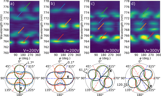
Figure 2. (a)–(d) Stark measurements in quadrupole electrode arrangement. The top row shows the different splitting patterns of the TS1 line for different electric fields as a function of the excitation polarization φ. The lower row displays the normalized intensity variations of the individual parts of the splitting pattern (colored arrows) represented as polar plot. The color of the data shown in the polar plot refers to the colored arrows in the spectra. The black arrow (E) represents the direction of the electric field applied; the red/blue dashed-dotted lines indicate the orientation of the principal crystallographic axes of 4H–SiC. For each column, the spectral lines exhibiting pronounced nodes are described by a cosine function (nodal black solid curve in the polar plots) in order to extract its polarization direction (φ0, small black arrow). This is complemented by the sum of another two cosine functions phase shifted by φ0 ± 120° to account for the two other symmetry equivalent directions (black solid curve with less pronounced nodal shape).
Download figure:
Standard image High-resolution imageFirst, we focus on the spectral lines at around 764 nm (red arrow) and 775 nm (green arrow) in figure 2(a) which exhibit explicit nodes around 90° and 270°. To characterize these lines further, we fit a  function to each line individually. Taking the mean value of the two fits yields the black solid line with φ0 = 1.7° ≈ 0° (polar plot) which describes both the red and green data excellently. Its orientation, that is φ0 ≈ 0, shows that these lines are maximized when both the electric field applied and the excitation polarization of the laser are aligned parallel to the
 ![$\left[\bar{1}100\right]$](https://content.cld.iop.org/journals/1367-2630/23/7/073002/3/njpabfb3eieqn6.gif) direction. The absolute orientations become visible in the polar plot: the blue and red dashed-dotted lines indicate the principal crystallographic axes; the black arrow indicates the direction of the static electric field. As the underlying SiC matrix has a threefold symmetry axis (c-axis), one expects fully equivalent transitions that are phase shifted by φ0 ± 120°. These lines can, indeed, be observed in the spectra of figure 2(a) even though they are partially overlapping (orange and blue arrow). Due to this overlapping, we plot the sum of the lines at around 766 nm and 767 nm (orange data in the polar plot) as well as their red-shifted symmetric counterparts around 772 nm and 773 nm (blue data in the polar plot) showing two lobes (orange, blue) with a significantly less pronounced waist than the red/green data. As the orange/blue data represents the sum of two spectral lines each, we investigate the data by plotting the sum of cos(φ + φ0 + 120°) and
direction. The absolute orientations become visible in the polar plot: the blue and red dashed-dotted lines indicate the principal crystallographic axes; the black arrow indicates the direction of the static electric field. As the underlying SiC matrix has a threefold symmetry axis (c-axis), one expects fully equivalent transitions that are phase shifted by φ0 ± 120°. These lines can, indeed, be observed in the spectra of figure 2(a) even though they are partially overlapping (orange and blue arrow). Due to this overlapping, we plot the sum of the lines at around 766 nm and 767 nm (orange data in the polar plot) as well as their red-shifted symmetric counterparts around 772 nm and 773 nm (blue data in the polar plot) showing two lobes (orange, blue) with a significantly less pronounced waist than the red/green data. As the orange/blue data represents the sum of two spectral lines each, we investigate the data by plotting the sum of cos(φ + φ0 + 120°) and  shown as black solid line maximized at approximately 90° in the polar plot, which describes the data accurately. This shows that the spectral lines displayed in figure 2(a) possess an obvious directedness of the optical transition within the basal plane, yielding three characteristic polarization directions phase shifted by 120° each.
The very same analysis scheme is applied after the electric field is rotated by 90° with respect to the c-axis. The obtained dataset is shown in figure 2(b); the analysis of the unsplit line around 769 nm (orange arrow) again yields a very similar number for φ0 = 0.1° ≈ 0°, which is in good agreement to figure 2(a). When adding again the sum of cos(φ + φ0 + 120°) and  to the polar plot (black solid line maximized around 90°), the intensity variations of the outer two spectral lines at around 764 nm (red arrow) and 775 nm (blue arrow) are well described. Note that this time, compared to figure 2(a), the outer two spectral lines in figure 2(b) (red and blue arrow) are not only partially but fully overlapping.
How different the patterns can be is further illustrated in figures 2(c) and (d). The electric field is now chosen with a ±45° tilt with respect to figure 2(b). We start with figure 2(c): compared to figure 2(b) the pattern looks entirely different as now the inner and outer, previously unsplit lines show splitting. Now, the inner two lines at around 768 nm (orange arrow) and 770 nm (blue arrow) show a polarization with φ0 = 61.1° ≈ 60°, expressed by a pronounced nodal shape. In addition, the equally weighted sum of the ±120° tilted replica (black solid line with less pronounced waist) of the cosine fit function describe the joint intensity of the outer spectral lines (red/green data) relatively well. Note that figures 2(c) and (d) are measured at the very same spatial position; only the electric field was tilted within the quadrupole. The comparison between figures 2(d) and (c) is interesting: The applied electric field differs by 90°, φ0 differs by 60° (now φ0 = 61.1°), and the spectra look approximately identical except for the relative phases of the spectral lines. The similarity of figures 2(c) and (d) is a consequence of the threefold rotation symmetry of the crystal lattice: while in figure 2(c) the E-field vector forms an angle of approximately 15° with the crystallographic axis at 330° in the polar plot (blue dashed line), it does so for the crystallographic axis at 210° in figure 2(d). This represents a physically equivalent situation, provided that different crystallographic directions are addressed by the Stark effect causing the interchanging of the inner and outer lines in figures 2(c) and (d), respectively.
Another way of displaying this inner symmetry is a mirror image of the polar plot in figure 2(c) with respect to the horizontal axis (90° or 270°), which results in a picture fully equivalent to figure 2(d). Altogether, modulo a built-in 60° symmetry of the ensemble of point defects, the four datasets in figure 2 provide characteristic symmetry-broken spectral splitting patterns in 15° steps. Although a systematic description of the data is provided, we see a small deviation of the smeared-out lobe in figures 2(c) and (d) from the data (red/green), which we can currently not explain.
Altogether, not only a strong response to the electric field but also three distinct polarization directions are observed for the TS1 line. The fact that a splitting pattern with exactly six lines (three blue-shifted, three red-shifted) can be generated using an electric field, while each individual line is considered to be non-degenerate (cf figures 1(c)–(e)), indicates that the underlying defect is orientationally degenerate, i.e. it exists for three different directions within the crystal matrix. This should guide our search for a microscopic model of the yet unknown TS defect, which consequently must involve several lattice sites. The strong response of the TS1 line to an applied electric field can be related to a significant difference vector  between the electric dipole moment associated with the ground state (|g〉) and the excited state (|e〉) [11]. Note that there are six such orientations for Δd (three possible directions times two signs of the vector, i.e. ±Δda,b,c) in the basal plane due to the crystal's threefold symmetry. This immediately explains the observed number of six shifted lines for a response of type hΔν ∝Δd ⋅ E (where E is the E-field vector and hΔν is the change in energy of the transition). From the angular analysis we can determine that Δd is oriented parallel to the crystal's
 ![$\left[\bar{1}100\right]$](https://content.cld.iop.org/journals/1367-2630/23/7/073002/3/njpabfb3eieqn10.gif) axis and their equivalents. That is, remarkably, a direction perpendicular to the bond direction of the constituent tetrahedra: there is no nearest neighbor in the crystal that is aligned with this direction. However, the connecting line between next-nearest neighbors points is the same direction as Δd. In the representation of figure 1(b) this would correspond to the directions that are given by nearest neighbors of the red sub-lattices (Si sites) or the black sub-lattice (C sites) within one basal plane. In the supplementary material (https://stacks.iop.org/NJP/23/073002/mmedia), we discuss the evolution of the six individual Stark shifted lines on a purely geometrical basis which reproduces the experimental findings nicely, see figure S1.
axis and their equivalents. That is, remarkably, a direction perpendicular to the bond direction of the constituent tetrahedra: there is no nearest neighbor in the crystal that is aligned with this direction. However, the connecting line between next-nearest neighbors points is the same direction as Δd. In the representation of figure 1(b) this would correspond to the directions that are given by nearest neighbors of the red sub-lattices (Si sites) or the black sub-lattice (C sites) within one basal plane. In the supplementary material (https://stacks.iop.org/NJP/23/073002/mmedia), we discuss the evolution of the six individual Stark shifted lines on a purely geometrical basis which reproduces the experimental findings nicely, see figure S1.
The above-mentioned orientational degeneracy of the TS defect cannot only be removed by an applied electric field but also by local strain. This can be seen in figure 3: figure 3(a) shows a spatially resolved series of spectra of the TS1 line that is performed in the vicinity of an intentionally introduced surface scratch in the (0001) plane. The scratch was generated by hand using a diamond scratch pen (see sketches in figures 3(a) and 4(a)). One observes the TS1 line splitting into three lines next to the surface scratch, which converge at larger distances (≈0.1 mm). The same scan performed for the TS2,3 lines is displayed in figure 3(b). There are irregularities in each curve which presumably stem from extended defects that are introduced along with the overall strain-field. Remarkably, each of the irregularities occurring in the spectral evolution of the TS1 have replica in both of the TS2,3 lines. Figures 3(c) and (d) show the excitation and emission polarization of the split TS1 line, respectively. As previously mentioned for the Stark measurements, we again observe three clear polarization directions of the TS1 transitions in absence of electric fields. Here, in contrast to the Stark measurements, there are three instead of six lines observable. For an oriented defect it is not surprising that the three different directions give a different spectral response to the strain field. However, their relative orientation to the strain-field (±) does not matter, presumably because the strain gradient is rather weak. In that sense, local strain cannot remove the orientational degeneracy of the TS defect completely.

Figure 3. (a)–(b) Spatially resolved PL scans in the vicinity of a surface scratch in the (0001) plane for the TS1 (a) and TS23 (b) lines, respectively. The inset indicates the orientation between the c-axis, the incident laser and the surface scratch. (c) And (d) displays the excitation/emission polarization of the three split lines for TS1.
Download figure:
Standard image High-resolution image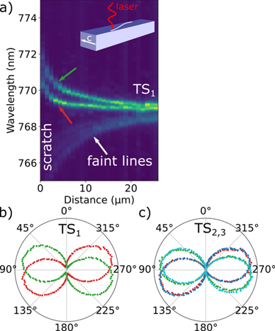
Figure 4. (a) Spectroscopy from the wafer edge: Spatially resolved PL scan in the vicinity of a surface scratch in the  plane (a-face) for the TS1 line. The inset indicates the orientation between the c-axis, the incident laser and the surface scratch. Faint lines (white arrow) show an opposite line shift compared to the brighter lines (red/green arrow), they are not further considered. (b) And (c) displays the emission polarization of the two predominant split lines belonging to TS1/TS23.
Download figure:
Standard image High-resolution imageTo gain a better understanding of the three-dimensional structure of the TS defect we now focus on PL measurements with the incident laser perpendicular to the crystal's c-axis. For this purpose, we cut a small strip out of the wafer, which is rotated in order to perform PL studies from the side wall, i.e. the  plane (a-facet). Figure 4(a) shows an analogue measurement to that of figure 3(a) with the rotated sample, where the scratch now is located on the a-facet. Again, we observe a splitting of the TS1 line next to the surface scratch. However, compared to figure 3(a), now two dominant split lines appear that are pointing upwards, along with a rather diffuse PL signature pointing downwards. The upper two lines (red and green arrow) show a clear (emission) polarization dependence displayed in figure 4(b). Here, φ = 0° corresponds to the c-axis, determined by comparison with the well-known polarization of the V1 line (not shown) [25]. Figure 4(b) shows that the polarization of the TS1 line lies within the basal plane (90° tilted with respect to the c-axis) where the two split lines (red/green) appear tilted by roughly ±15°. This tilt is equally observed when studying the polarization dependence of the TS2,3 lines at the very same spot: figure 4(c) shows the (emission) polarization of the four split TS2,3 lines (red/green, blue/cyan), which can barely be distinguished from the polarization plot. Note that for the measurement regarding figures 3 and 4 a different excitation wavelength (635 nm diode laser) was used for technical reasons.
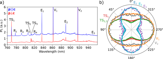
So far, we could present a thorough study of the TS's response to strain and electrical fields. We now turn to an accompanying observation of extra lines appearing during spectroscopy from the side wall. Figure 5(a) shows two PL spectra with the incident laser being perpendicular to the c-axis of the sample. The red/blue curve displays a PL spectrum for which the laser polarization vector p is perpendicular/parallel to the c-axis, represented as p⊥c and p∥c, respectively. Note that the blue spectrum is artificially shifted upwards for better visibility. In contrast to the spectra with the incident laser being parallel to the c-axis, the spectra in figure 5(a) show obvious differences: three spectral lines appear at 836.7 nm, 889.7 nm and 949.9 nm (termed E1, E2 and E3, respectively) which are absent when looking from the (0001)-facet. Figure 5(b) displays the excitation polarization of the TS, E and V lines (VSi) shown in figure 5(a) where φ = 0° again corresponds to the orientation of the c-axis. It clearly indicates that the E lines all share the same polarization characteristic pointing along the c-axis, that is perpendicular to that of the TS lines.
Figure 5. (a) PL spectra with the incident laser being perpendicular to the c-axis. The laser polarization (p) is perpendicular/parallel to the c-axis for the red/blue curve. (b) Polar plot of the excitation polarization dependence of the TS, E and V lines shown in (a). The E lines show a clear polarization characteristic perpendicular to that of the TS lines.
Download figure:
Standard image High-resolution image
The E lines appear under very similar sample preparation conditions as the TS lines: (i) even for unprocessed samples TS lines can be observed as a small signal, but only close to the Si-face of the crystal, when performing spectroscopy from the side wall. Their PL intensity then tends to fade away with increasing distance from the Si-edge such that they cannot be observed at greater distances than a few ten microns. The same holds true for the E lines in our experiments. (ii) After proton irradiation and annealing at 1200 °C, the TS as well as the E lines can be generated homogeneously all over the sample area with the resulting PL intensities scaling with the initial irradiation dose. (iii) Performing spatially resolved PL scans across the implantation edge, one observes an equally sharp PL intensity drop for the E lines as for the TS lines. Another common observation is that energetic shift of the zero-phonon line positions of the TS1, E1 and E2 lines (TS2,3 and E3 lines could not be resolved) with increasing sample temperature is very similar and is significantly different from that of the V lines. For the mentioned findings, we expect a connection between the defect responsible for the TS lines and that responsible for the E lines which we can currently however not pin point. Finally, there is a signature that shows up in figure 5(a) as a series of lines, termed 'R-lines', the sharpest of which appears at 777.7 nm. Remarkably, they are equidistant in energy: R1/R2, R2/R3 and R3/R4 each differ by about 27 meV, and the lower the energy is, the broader the resonance appears. The further investigation of those lines lies beyond the scope of this paper and is therefore relegated to future work.
In summary, we present a detailed PL study of the structurally yet unknown TS color center, in which we study the spectral response of the TS defect with respect to applied electric and strain fields. The TS1 transition possesses three distinct polarization orientations within the basal plane of the crystal. Each individual orientation, in turn, comprises two opposite directions of the associated electric dipole moment vector Δd, responding oppositely under the influence of an applied electric field. These findings imply that the underlying defect is a low-symmetry complex involving several lattice sites, which does not point along the basal bond directions but along the next-nearest neighbor directions. We find a counterpart spectral feature, the E lines, which have an out-of-plane orientation. This study thus provides important detail information that should enable the atomistic identification of the TS defect.
Acknowledgments
This work was funded by the Deutsche Forschungsgemeinschaft (DFG, German Research Foundation) – Project-ID 429529648 – TRR 306 QuCoLiMa ('Quantum Cooperativity of Light and Matter'). We acknowledge fruitful discussions with Takuma Kobayashi, and Brett Johnson.
Data availability statement
The data that support the findings of this study are available upon reasonable request from the authors.