


Abstract
AlAs is a semiconductor that can form heterostructure, superlattice, and ternary alloy with GaAs. We systematically investigate the formation energies, transition energy levels, as well as defect and carrier densities of intrinsic defects and extrinsic impurities in AlAs using first-principles simulations. Most of the intrinsic defects, including vacancies, antisites and interstitials, show similar features as those of GaAs. Intrinsic defects are found not to be the origin of the n-type or p-type conductivity due to their high formation energies. For extrinsic dopants (Si, C, Mg and Cu), Mg can be an effective p-type dopant under both As-rich and As-poor conditions. Si-doping can introduce either n-type or p-type, depending on the specific growth condition. C serves as a p-type dopant under As-poor and As-moderate conditions, and Cu-doping has little effect on the conductivity.
Export citation and abstract BibTeX RIS

Original content from this work may be used under the terms of the Creative Commons Attribution 4.0 licence. Any further distribution of this work must maintain attribution to the author(s) and the title of the work, journal citation and DOI.
1. Introduction
Zinc-blende AlAs is a III–V semiconductor that has not only the same crystal structure and nearly same lattice constant with GaAs, but also a wider band gap (2.16 eV vs 1.42 eV), making AlAs and GaAs an excellent semiconductor pair to grow alloys [1], heterostructures [2, 3] and superlattices [4]. Due to the superb miscibility and high carrier mobility of GaAs and AlAs, these structures can be applied in high-speed digital, high-frequency microwave, electronic and electro-optic devices [1, 4], such as high electron mobility transistors [1, 3, 4] and quantum well infrared photodetectors [5].
As defects and impurities inevitably exist in the semiconductors, their effects on the electronic and optical properties are essential for the performance. First-principles simulations can provide rich theoretical insights for understanding the defects and impurities [6–12]. The defect properties of AlAs/GaAs alloy and heterostructure, as well as GaAs have been extensively studied [13–19], however, a systematic study of defects in AlAs has not been reported yet. Jiang et al [16] investigated six types of intrinsic defects of AlAs in their neutral states, including interstitials (Ali and Asi), antisites (AlAs and AsAl), and vacancies (VAl and VAs). It was found that the neutral AsAl antisite has the lowest formation energy among these defects, but the defects in charged states, which normally have significant impact, were not considered. Chroneos et al [20–23] studied more intrinsic defects with more charge states using Perdew–Burke–Ernzerhof (PBE) and local-density approximation functionals, but the underestimated band gap may introduce inaccuracy into the defect calculations. Besides the intrinsic defects, extrinsic dopants/impurities may have a significant effect on the properties. Spectrographic analysis reveals that AlAs can be mostly contaminated by Si, as well as Mg, and Cu impurities [24]. Their properties such as formation energies and transition energy levels have not been investigated theoretically. Moreover, both n-type and p-type conductivity have been observed in AlAs samples with these extrinsic dopants [24–30], however, the origins of such conductivities have not been well understood from a theoretical perspective. Overall, a systematic study of the intrinsic and extrinsic defects in AlAs is in need for better understanding of the electronic and optical performance of AlAs and related semiconductors.
In this work, we systematically study the intrinsic defects and dopants (Si, C, Mg and Cu) in AlAs using first-principles calculations. Three chemical conditions including As-rich (Al-poor), As-moderate and As-poor (Al-rich) are considered. Our results show that most of the intrinsic defects, including vacancies, antisites and interstitials, exhibit similar properties as GaAs. All intrinsic defects are determined to have low concentrations. Neither n-type nor p-type conductivity is predicted to exist in AlAs with merely intrinsic defects considered, however, doping of extrinsic element Si makes the materials n-type or p-type, and C and Mg doping makes it p-type. Doping of Cu leads to weak n-type conductivity. Our finding explains the origin of the measured n-type and p-type conductivity in AlAs samples containing Si [24–26], and the strong p-type conductivity induced by C- and Mg-doping in other experiments [27–30]. We also predict that Cu-doping is not the source of p-type or n-type conductivity in previous experiments [24].
2. Computational details
Our first-principles simulations based on density functional theory (DFT) [31, 32] are performed using the Vienna ab initio simulation package [33–35]. The PBE [36] and Heyd–Scuseria–Ernzerhof (HSE06) [37] exchange–correlation functionals are adopted for structural optimization and electronic structure calculation, respectively. Based on PBE functional, HSE06 functional replaces 25% short-range exchange with Hartree–Fock exact exchange, and the range-separation parameter is selected as 0.11 bohr−1. The projector augmented waves method is utilized to treat the atomic core regions [38]. The cutoff energy is chosen as 400 eV, and a 216-atom supercell is used to simulate the defects. The first Brillouin zones of the primitive cell and the supercell are sampled by 2 × 2 × 2 and 1 × 1 × 1 Monkhorst–Pack [39] k-point mesh, respectively. Spin polarization is considered for charge states with unpaired spins. The energy convergence of electronic steps is set as 10−5 eV.
In terms of defects, the formation energy ΔHf(α,q) of a point defect α with charge state q is determined by

where  . E(host) and E(α,q) are the total energies of the supercells without and with defect α, respectively. ni
is the number of type-i defect atoms, and μi
and Ei
are the chemical potential and energy per i element in its pure phase. For charged defects, ΔHf(α,q) depends on not only the Fermi level EF, which is referenced to the valence band maximum (VBM), or εVBM(host), but also the chemical potentials of component elements. The potential alignment and image charge correction are used in the calculation of the energies of charged defects [40, 41].
. E(host) and E(α,q) are the total energies of the supercells without and with defect α, respectively. ni
is the number of type-i defect atoms, and μi
and Ei
are the chemical potential and energy per i element in its pure phase. For charged defects, ΔHf(α,q) depends on not only the Fermi level EF, which is referenced to the valence band maximum (VBM), or εVBM(host), but also the chemical potentials of component elements. The potential alignment and image charge correction are used in the calculation of the energies of charged defects [40, 41].
There exist several thermal dynamic conditions of the chemical potentials for the growth of the material under equilibrium. To avoid Al, As and other involved elements X forming their elemental phases, it is required that

In addition, AlAs should be stable under equilibrium, meaning

In equation (3), ΔHf(AlAs) is the formation energy of the compound AlAs.  is calculated as −1.2787 eV, which is consistent with the experimental values around −1.26 eV [42–44]. Furthermore, the formation of other possible secondary compounds involving the host and dopant elements, or Alm
Xn
and Xn
Asm
, should also be avoided, which requires
is calculated as −1.2787 eV, which is consistent with the experimental values around −1.26 eV [42–44]. Furthermore, the formation of other possible secondary compounds involving the host and dopant elements, or Alm
Xn
and Xn
Asm
, should also be avoided, which requires

and

For instance, the formation energy of SiAs2 is −1.24 eV, so the highest possible μSi is −1.24 eV under As-rich condition (μAs = 0, μAl = −1.28 eV) and 0 eV under Al-rich condition (μAs = −1.28 eV, μAl = 0). The sample will have no residue of the secondary compounds for instance SiAs2 in the Si-doped AlAs only when these chemical potential conditions are met.
The carrier concentrations are investigated using the approach as described in reference [45]. The hole and electron concentrations are given by

where Eg is the band gap of AlAs (2.16 eV). kB is Boltzmann constant, and T is temperature. Nv and Nc are the effective densities of states of the valance bands and conduction bands, respectively. Nv and Nc are given by

The effective mass of hole (m*p) and electron (mn*) are 0.195 m0, and 0.517 m0, respectively. The charge neutrality condition without dopants satisfies

In case of doping, with the concentrations of acceptors N − A and donors N + D, the charge neutrality condition gives

By solving this equation, we can obtain the Fermi energy and hole/electron concentrations at equilibrium as a function of temperature and dopant concentrations.
Finally, defect concentration for defect α in charge state q is given by

where Nsites is the density of possible atomic sites of defects. gq is degeneracy factor [45].
3. Results and discussion
3.1. Electronic structure
For zinc-blende lattice of AlAs, the lattice parameter is calculated as 5.67 Å using HSE06, agreeing with the experimental value of 5.66 Å [46]. The calculated Al–As bond length is 2.48 Å. Based on the optimized structure, we further calculate the electronic band structure as well as the density of state (shown in figure 1). AlAs exhibits an indirect bandgap of 2.16 eV, with VBM located at Γ point, and the conduction band minimum (CBM) located at X point (0.5, 0.5, 0). Our calculated band gap size is highly consistent with the experimental values 2.23–2.25 eV [47–49].
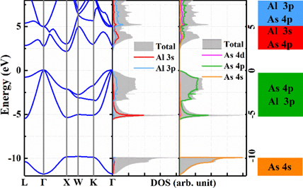
Figure 1. HSE06-calculated band structure of AlAs, total density of states (DOS), and projected DOS of AlAs. The electronic orbitals that contribute to the bands are indicated by color blocks.
Download figure:
Standard image High-resolution imageThe orbital-projected density of state is displayed in figure 1. The valence band is mostly composed of Al–3p and As–4p orbitals, whereas the conduction band is mainly contributed by Al–3s, Al–3p and As–4p electrons.
3.2. Intrinsic defects
The calculated formation energies as functions of the Fermi level under As-rich conditions are shown in figure 2(a). Among all the defects, AsAl 2+ is found to have the lowest formation energy when the Fermi level is close to VBM. Its positive charge state indicates that it is a donor defect. As Fermi level increases to 0.53 eV and 1.02 eV, its charge state transits to 1+ and neutral states, respectively. The (−/0) transition energy level is found to be comparatively close to CBM. With Al substituted by As, the Al–As bonds are broken, and the As 4p states in the conduction band (figure 1) move down, leading to the deep (+/2+) and (0/+) defect levels in the middle of the gap. For Fermi level higher than 1.87 eV above VBM, VAl 3– is determined to have the lowest formation energy, while the AsAl becomes the second favorable defect. In this regime, VAl 3– serves as an acceptor and a significant donor-passivating defect. Its (2−/0) and (3−/2−) transition energy levels lie at 1.40 eV and 1.01 eV below the CBM, respectively. The transition energy levels of the main defects are also summarized in figure 3.

Figure 2. Formation energies of intrinsic defects in AlAs as a function of Fermi level (EF) under (a) As-rich (Al-poor) and (b) As-poor (Al-rich) conditions. (c) Fermi energy, concentrations of defects and carriers at 300 K for intrinsic AlAs as a function of μAs from As-rich to As-poor.
Download figure:
Standard image High-resolution image
Figure 3. Summary of the transition energy levels of the intrinsic point defects in the band gap of AlAs.
Download figure:
Standard image High-resolution imageUnder the As-poor condition, as shown in figure 2(b), Ali is the defect that has the lowest formation energy for Fermi energy between VBM and 0.98 eV above. Ali bonds with the neighboring As (Al – As bond length is 2.48 Å), as well as a nearby Al (Al–Al bond length is also 2.48 Å). The (2+/3+) transition energy level of Ali is approximately 0.73 eV above the VBM, as shown in figure 3. The formation energy of Ali
0 is lower than that of Asi
0 under As-poor condition, which is similar to the formation of  being lower than
  in GaAs under the same condition [16]. AlAs becomes the defect with lowest formation energy for Fermi energy between 0.98 eV and CBM. Other defects and defect clusters (VAs–VAl, AlAs–AsAl and Asi) have much higher formation energies in both As-rich or As-poor cases, and thus their concentration is very low.
Following equations (6)–(10), we calculate the Fermi energy, concentrations of defects and carriers at 300 K as a function of the chemical potentials μAs. As shown in figure 2(c), although the maximum concentrations of AsAl
0 and VAs
0 are 1016 cm−3 and 1014 cm−3 respectively, neutral defects have no effect on carrier concentration and conductivity. The Fermi level and carrier density show nonmonotonic behavior between As-moderate and A-poor condition, which is caused by the rising of the  . The electron concentration at any chemical potential μAs is determined to be relatively low (103–108 cm−3), which is not only caused by Fermi level being pinned moderately above the middle of the band gap, but also the high formation energies of the intrinsic defects under both As-rich and As-poor conditions (figure 2). Such low carrier density indicates the non-conductivity in AlAs with only intrinsic defects considered. It also indicates that the experimentally observed conductivity comes from impurities [24–26] rather than intrinsic defects.
3.3. Extrinsic dopants/impurities
We also study the common impurity defects, such as Si, C, Mg and Cu. These impurities are found in the sample during growth and postprocessing [24–26]. Our discussion below will reveal that Mg can be an effective p-type dopant, only Si doping under the As-rich or As-moderate conditions can introduce high n-type conductivity, while other dopants, e.g. C leads to p-type conductivity. In addition, Cu doping has relatively weak effect on conductivity.
3.3.1. Si and C doping
The formation energies of Si-doping, as well as some important intrinsic defects are summarized in figure 4. Under As-rich condition, as plotted in figure 4(a), SiAl 1+ is determined to have the lowest formation energy between 0.36 and 1.20 eV above VBM, taking over the place from AsAl in this Fermi level range. Formation energy of SiAl is generally lower than those of SiAs and Sii, indicating that the Si impurities mostly exists in the form of SiAl under As-rich condition. As presented in figure 4(a), the (−/+) transition energy level is of SiAl is 0.12 eV below the CBM. SiAl is an acceptor above this level while a donor below this level.
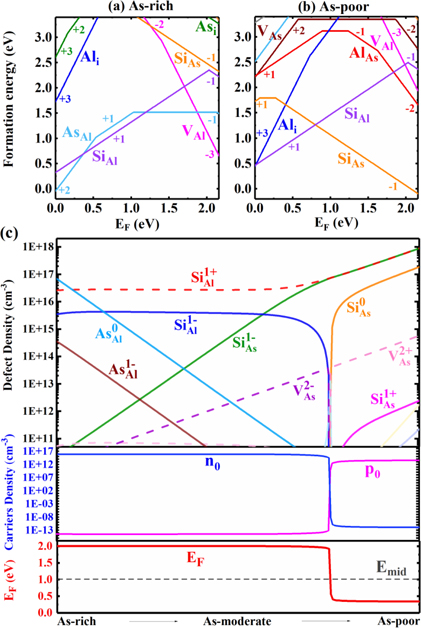
Figure 4. Formation energies of Si-doped AlAs as a function of Fermi level under (a) As-rich and (b) As-poor conditions. (c) Fermi energy, concentrations of defects and carriers at room temperature for Si-doped AlAs as a function of μAs from As-rich to As-poor.
Download figure:
Standard image High-resolution imageUnder As-poor condition, as shown in figure 4(b), SiAl 1+ is a donor defect that has the lowest formation energy defects for Fermi energy between VBM and 0.80 eV above. In the rest energy range, SiAs 1− is the most energetically favorable. SiAs is a donor when the Fermi level is near VBM, and serves as an acceptor in a larger Fermi level range above the (−/0) transition energy level.
Figure 4(c) shows the defect and carriers concentrations as functions of μAs for Si-doping. Si-doped AlAs exhibits n-type conductivity under As-rich and As-moderate condition. The densities of electron carrier is calculated to be around 2 × 1016 cm−3 under As-rich and As-moderate condition, one order of magnitude lower than the measured values in experiments (6 × 10¹⁷–8.5 × 1017 cm−3) [24, 25]. The SiAl 1+ concentration is around 1017 cm−3 under aforesaid condition, also slightly less than the measured values in experimental values (1018 cm−3) [24]. High electron carrier density in Si-doped AlAs indicates its strong n-type conductivity. Si-doping pushes the Fermi level close to the CBM under the As-rich and As-moderate condition [figure 4(c)]. Under As-poor condition, the SiAs 1− acceptor and the SiAl 1+ donor correspond to their lowest formation energies. Fermi level is relatively close to VBM level, leading to the relatively weak p-type conductivity. Therefore, the conductivity transits from strong n-type to weak p-type as μAs decreases to As-poor condition.
For C doping, intrinsic defects have lower formation energies than most of C-induced defects, such as Ci and CAl under As-rich condition [figure 5(a)]. The C-induced defect with the lowest formation energy is CAs. CAs has a (0/+) transition energy level at 0.02 eV and a (−/0) level at 0.19 eV in figure 8. Defects CAl and Ci have much higher formation energies in both As-rich or As-poor conditions, so they have low impact on the carrier densities. Under As-poor condition [figure 5(b)], intrinsic defect Ali 3+ has the lowest formation energy between VBM and 0.50 eV above, and CAs 1– take over for Fermi levels higher than 0.50 eV above VBM. The defects concentration as a function of μAs are plotted for C-doping in figure 5(c). The highest concentration of CAs 1– defect is in the order of 1016 cm−3 for most of the μAs values. Under As-poor and As-moderate conditions, the Fermi level is pinned at around 0.18 eV above VBM, indicating that the conductivity is p-type under this condition. The hole density of 2 × 1016 cm−3 [see figure 5(c)] in As-poor condition is smaller than the values (1019 cm−3) measured in Raman, photoluminescence spectroscopy and other experiments [28–30].
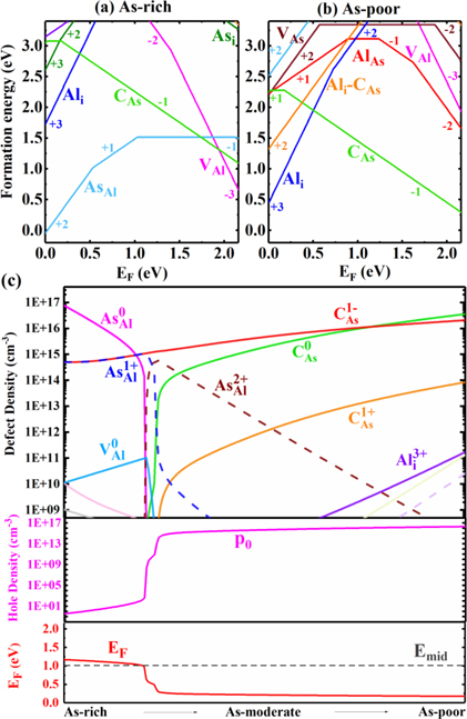
Figure 5. Formation energies of C-doped AlAs as a function of Fermi level under (a) As-rich and (b) As-poor conditions. (c) Fermi energy, concentrations of defects and carriers at room temperature for C-doped AlAs as μAs changes from As-rich to As-poor.
Download figure:
Standard image High-resolution image3.3.2. Mg and Cu doping
Figure 6 shows the formation energies of defects related to Mg doping, as well as the intrinsic defects. Mg-doping mainly introduces two types of defects, Mgi 2+ and MgAl 1−, with lower formation energies than intrinsic defects. Under both conditions, the defect with lowest formation energy is Mgi 2+ for Fermi energies on the VBM side, while it transits to MgAl 1− on CBM side. The energies for this transition are 0.26 eV and 0.67 eV above VBM for As-rich and As-poor conditions, respectively.

Figure 6. Formation energies of Mg-doped AlAs as a function of Fermi level under (a) As-rich and (b) As-poor conditions. (c) Fermi energy, concentrations of defects and carriers at room temperature for Mg-doped AlAs as μAs changes from As-rich to As-poor.
Download figure:
Standard image High-resolution imageMgAl is an acceptor in most part of the Fermi level range. Its (0/+) and (−/0) transition energy levels lie at 0.02 eV and 0.19 eV above the VBM, respectively, as shown in figure 8. The MgAl 1− concentration is 1019 ∼ 1022 cm−3, higher than the experimental value (2 × 1017 cm−3) [24]. MgAl 0 concentration is also high, but neutral state does not contribute to electrical conductivity. The concentration of Mgi 2+ is calculated to be significantly high (9 × 1021 cm−3) under As-rich condition, due to its low formation energies [figure 6(c)]. Meanwhile, it should be noticed that the carrier (hole) density (6 × 1015 cm−3) of Mg-doping, and its Fermi level is pinned 0.27 eV above VBM. Thus, Mg-doping is a suitable way to improve the p-type conductivity, which is similar to Mg-doped GaAs in experiments [50, 51].
For Cu-doping, the formation energies of Cu-doping as a function of Fermi level are shown in figures 7(a) and (b), as well as charge transition energy levels of Cu-doping in AlAs as presented in figure 8. Under As-rich condition [figure 7(a)], CuAl 2− emerges with the lowest formation energy between 1.01 eV above VBM and CBM, whereas Cui 1+ has slightly lower formation energy than the lowest intrinsic AsAl for a small energy range in the middle of the band gap. Under As-poor condition in figure 7(b), Cui 1+ and CuAl 2− exhibit lower formation energies than all intrinsic defects for Fermi energy higher than 0.16 eV above VBM. As shown in figure 7(c), the densities of CuAl 1− and Cui 1+ both decreases monotonically from 1017 cm−3, as μAs varies from the As-rich to As-poor condition. The calculated Cu concentration (1017 cm−3) agree with the detected values in experiments (8.4 × 1017 cm−3) [24]. CuAl 2− and Cui 1+ pin the Fermi level at 0.70 eV below the CBM under As-poor condition, while it makes the Fermi level not close to CBM under As-rich condition. The carrier (electron) density of Cu-doping is 6 × 1012 cm−3 under As-poor condition, while it is close to 0 under As-rich condition. As a result, the conductivity is barely affected by Cu-doping under As-rich condition, while weakly n-type conductivity is introduced by Cu-doping under As-poor condition.

Figure 7. Formation energies of Cu-doped AlAs as a function of Fermi level under (a) As-rich and (b) As-poor conditions. (c) Fermi energy, concentrations of defects and carriers at room temperature for Cu-doped AlAs as μAs changes from As-rich to As-poor.
Download figure:
Standard image High-resolution image
Figure 8. Charge transition energy levels of four dopants (Si, C, Mg and Cu) in AlAs.
Download figure:
Standard image High-resolution image
4. Conclusion
In summary, we have investigated the formation energies, transition energy levels, and the defect and carrier concentrations of the intrinsic defects and several common extrinsic dopants in AlAs. For intrinsic defects, AsAl and VAl are determined to have the lowest formation energies under As-rich condition, whereas Ali and AlAs have the lowest formation energies with different Fermi energy range under As-poor condition. Though their formation energies are calculated to be lower than other intrinsic defects, they are still generally high, causing low defect concentrations. As a result, the intrinsic defects cannot be the source of n-type or p-type conductivity. For extrinsic doping, doping of Si, C, Mg, and Cu all shows lower formation energies for related defects depending on the growth chemical conditions, leading to higher defect and carrier concentrations. Si-doping introduces high electron concentration and n-type conductivity under As-rich condition, and high hole concentration and p-type conductivity under As-poor condition. C-doping can make AlAs p-type conductive under As-poor and As-moderate conditions, while Mg is an efficient p-type dopant under any growth condition. In addition, Cu is not an effective n-/p-type dopant according to our calculations. Our results provide insights for optimizing the performance of the AlAs-related semiconductors.
Acknowledgments
This work was supported by National Natural Science Foundation of China (NSFC) under Grant Nos. 61722402 and 91833302, Shanghai Academic/Technology Research Leader (19XD1421300), Eastern Scholar Program, Fok Ying Tung Education Foundation (161060) and the Fundamental Research Funds for the Central Universities.
Data availability statement
The data that support the findings of this study are available upon reasonable request from the authors.