


Abstract
Manipulating the valley degree of freedom as an information carrier has been a focused topic for both fundamental and applied research. Here, using first-principles calculations, we report the identification of monolayer CrX2 (X = S, Se) as a novel two-dimensional valleytronic crystal. It shows large valley spin splitting in the valence band, attractive for the integration of valleytronics and spintronics. More importantly, through proximity coupling with monolayer CrCl3, the valley polarization in monolayer CrX2 is achieved, which can be further engineered by stacking patterns. Also, the valley polarization in monolayer CrX2 can be obtained via magnetically doping V and Mn. Specially for V-doped monolayer CrSe2, there are no impurity states in the band gap, beneficial for its practical applications. Our works thus provide not only exceptional two-dimensional valleytronic crystals but also promising ways for realizing valley polarizations in them.
Export citation and abstract BibTeX RIS

Original content from this work may be used under the terms of the Creative Commons Attribution 4.0 licence. Any further distribution of this work must maintain attribution to the author(s) and the title of the work, journal citation and DOI.
Introduction
Two-dimensional (2D) valleytronic materials have recently attracted considerable attention [1, 2] with the development of 2D materials [3–8]. In 2D valleytronic materials, the valley characterizes the local maximum in the valence band or the local minimum in the conduction band at the K and K' points. Therefore, carriers are endowed with an extra degree of freedom, namely the valley index, which is robust against lattice scatting as it has large separation in momentum space [9]. Also, the valley index is associated with the valley-contrasting physical quantities [2]. Analogous to exploiting charge for electronics or spin for spintronics [10, 11], the valley index constitutes the binary states, forming the main context of valleytronics. This results in a large amount of intriguing phenomena and potential applications, especially in information storage and processing [12–15]. Although 2D valleytronic materials are highly desirable, up to now, only a few candidates are proposed, including graphene, VSSe, Tl2O, and 2D transition metal dichalcogenides (TMDs) MX2 (M = V, Ta, Mo, W; X = S, Se, Te) [16–22]. Therefore, new 2D valleytronic materials remain to be discovered and are still urgently needed.
On the other hand, to make a valleytronic device, it is necessary to break the balance of carriers in the K and K' valleys, thereby achieving the valley polarization [9, 23]. To that end, currently, several avenues are proposed. One is to use the circularly polarized optical pumping [14, 15] since the orbital magnetic moments are opposite in the K and K' valleys. This approach has been well demonstrated in experiments to be able to realize valley polarization [13–15, 24–27]. However, optical pumping is a dynamical process, which simply changes the chemical potential in the valleys and is not applicable for robust manipulation [18]. Another avenue is to use magnetic field to induce spin polarization, which is accompanied by a valley polarization [28, 29]. That is because the spin and valley indexes in 2D valleytronic materials are locked to each other. Although valley polarization is indeed achieved by applying external magnetic field experimentally, the effect is rather modest as 1 T magnetic field can only lead to a splitting of 0.1–0.3 meV [30–32]. Compared with these two approaches, recently utilizing atom doping [20, 33–37] and magnetic semiconductor substrate [38–44] are shown to be more effective ways to achieve valley polarization. Nevertheless, as the interaction between host material and the substrate/doping may deform the valley feature, the magnetic substrate or transition metal must be selected carefully.
In this work, we systematically investigate the electronic and valleytronic properties of monolayer CrX2 (X = S, Se) on the basis of first-principles calculations. Monolayer CrX2 is a direct-gap semiconductor and harbors two inequivalent valleys at the K and K' points. Also, it exhibits a very large valley spin splitting in the valence band, providing a highly attractive candidate for research on valleytronics and spintronics. Moreover, we propose two effective strategies to produce valley polarization in monolayer CrX2, where the valley features are well preserved. One is through proximity coupling with monolayer CrCl3, which leads to valley polarization. And the induced valley polarization exhibits a stacking pattern-dependent behavior. Another is utilizing V and Mn doping. Particularly for the case of V-doped monolayer CrSe2, no impurity state appears in the band gap, which is favorable for practical applications. These compelling properties render monolayer CrX2 an attractive platform for developing valleytronic devices.
Methods
First-principles calculations are performed within density functional theory (DFT) as implemented in Vienna ab initio Simulation Package (VASP) [45]. To describe the electron-ion interaction, the projected augmented wave (PAW) approach is adopted [46]. The generalized gradient approximation (GGA) in form of Perdew–Burke–Ernzerhof (PBE) functional is used to describe the exchange-correlation interaction [47]. The cutoff energy is set to 500 eV. The vacuum space is set to be about 18 Å. The van der Waals interaction is treated by the DFT-D3 method [48]. Structures are fully relaxed with the force tolerance of 0.01 eV Å−1. The convergence criterion for electronic iteration is set to be 10−6 eV. A 7 × 7 × 1 and 9 × 9 × 1 k-point grid is used to sample the Brillouin zone for geometry optimization and static electronic calculations, respectively. The strong-correlated correction is considered with GGA + U method to deal with the Cr's 3d electrons [49]. The effective onsite Coulomb interaction parameter (U) and exchange interaction parameter (J) are set to be 3.5 and 0.5 eV, respectively [20, 50–52]. The spin–orbit coupling (SOC) effect is taken into account in electronic structure calculations. Berry curvatures are calculated using the WANNIER90 package [53]. The phonon spectra is obtained using the PHONOPY code [54].
Results and discussion
It is known that CrX2 can exist in 2H phase and 1T phase [55, 56]. Previous works investigated the electronic and magnetic properties of 1T-CrX2 and found that a strain can induce a state switch between ferromagnetic and antiferromagnetic [56]. However, the inversion symmetry limits its valleytronic applications. Here, we focus on 2H-CrX2 to investigate the valleytronic properties. Figure 1(a) shows the crystal structures of monolayer CrX2. It exhibits a hexagonal lattice, with a Cr atom layer sandwiched between two X atom layers. The lattice constants are found to be a = b = 3.041 Å for CrS2 and a = b = 3.173 Å for CrSe2, which agree well with previous works [55, 57, 58]. To confirm the stability of CrX2, we calculate its phonon spectra. As shown in figure S1, no imaginary frequency is observed in the whole Brillouin zone, indicating that CrX2 is dynamically stable. The crystal symmetry of monolayer CrX2 is D3h, and hence its inversion symmetry is explicitly broken. The band structures of monolayer CrX2 are shown in figures 1(d) and (e). We can see that monolayer CrS2 (CrSe2) is a semiconductor with a direct band gap of 0.93 (0.75) eV. The valence band maximum (VBM) and conduction band minimum (CBM) both locate at the at the K and K' points, forming two energy-degenerate valleys. By comparing the band structures with and without considering SOC, we can see an interesting point. Namely, upon including SOC, both VBM and CBM experience a valley spin splitting, and thus the spin degeneracy of both VBM and CBM are lifted (see figure 2(b)). And as shown in figures 1(d) and (e), the ordering of the spin-up and spin-down states at K and K' valleys are opposite, which can be attributed to the time-reversal symmetry [E↑(k) = E↓(−k)]. Accordingly, spin can be selectively excited through the optical selection rule.
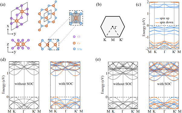
Figure 1. (a) Top and side views of the crystal structures of monolayer CrCl3 and CrX2. Right part in (a) shows the coordination environment of Cr atom in monolayer CrX2. (b) 2D Brillouin zone for monolayer CrX2 with marking the high-symmetry points. Band structures of monolayer (c) CrCl3, (d) CrS2 and (e) CrSe2. The blue and orange lines denote spin-up and spin-down states, respectively. The Fermi level is set to 0 eV.
Download figure:
Standard image High-resolution image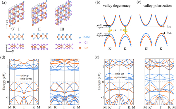
Figure 2. (a) Crystal structures of CrX2/CrCl3 heterostructure under different stacking configurations from top and side views. Schematic diagrams of the bands with SOC at the K and K' valleys for (b) monolayer CrX2 and (c) CrX2/CrCl3 heterostructure. The blue and orange lines in (b) and (c) denote spin-up and spin-down states, respectively. Band structures of (d) I-CrS2/CrCl3 and (e) I-CrSe2/CrCl3 without (left) and with (right) SOC. The blue and orange lines denote spin-up and spin-down states, respectively. The Fermi level is set to 0 eV.
Download figure:
Standard image High-resolution imageIt should be noted that the valley spin splitting in the valence band [68.5 (90.6) meV] of monolayer CrS2 (CrSe2) is significantly large, although these values are smaller than that of transition metal dichalcogenides (0.1–0.5 eV) [9, 35, 59]. In contrast, the valley spin splitting in the conduction band is extremely small [4.1 (15.4) meV]. Such a difference is sought into the different orbital contributions of the VBM and CBM of monolayer CrX2. As shown in figure S2, the VBM of monolayer CrX2 is mainly from the  orbitals of Cr and px,y orbitals of X. As Cs symmetry guarantees the out-of-plane potential gradient symmetry, the valley spin splitting in monolayer CrX2 mainly results from the in-plane potential gradient asymmetries. The in-plane character of these states combined with the strong SOC strength within the Cr atom results in the sizeable valley spin splitting in the valence band. While for the CBM, it is dominated by dz2 orbital of Cr. The out-of-plane orientation of dz2 orbital has slight impact on the valley spin splitting, resulting in the negligible value in the conduction band.
Having estimated the K and K' valleys of monolayer CrX2, we then explore how to generate and manipulate its valley polarization, which is indispensable for developing valleytronic devices. We first utilize magnetic proximity coupling in heterostructures composed of monolayer CrX2 and a magnetic substrate to lift the valley degeneracy. Here, monolayer CrCl3 is selected as the substrate due to two considerations. First, monolayer CrCl3 has been well identified to be a magnetic semiconductor. And as shown in figure 1(c), it has a large direct band gap of 1.51 eV. Second, the lattice mismatch between them is small. The CrX2/CrCl3 heterostructure is constructed using a 2 × 2 supercell of CrX2 and a 1 × 1 unit cell of CrCl3, which results in a lattice mismatch of 0.24% for CrS2/CrCl3 and 2.37% for CrSe2/CrCl3. To reveal influences of lattice mismatch on the magnetic coupling, we also investigate the band structures of I-CrX2/CrCl3 under strain of ±1%. As shown in figure S3, the lattice mismatch has little effect on the magnetic coupling between CrX2 and CrCl3. Such tiny mismatches are well desirable for experimental explorations. Moreover, bulk CrCl3 has been successfully exfoliated down to the monolayer limit [60, 61], offering the possibility for creating van der Waals heterostructures.
For CrX2/CrCl3 heterostructure, we consider three typical configurations, including I-CrX2/CrCl3 (two X atoms are above one Cr atom of CrCl3), II-CrX2/CrCl3 (one Cr atom of CrX2 is on top of the Cr atom of CrCl3) and III-CrX2/CrCl3 (two X atoms and one Cr atom of CrX2 are above two different Cr atoms of CrCl3); see figure 2(a). To estimate the relative stability among these configurations, we calculate their binding energies, which are defined as  Here
Here  and
and  represent the energy of CrX2/CrCl3 heterostructure, monolayer CrX2 and monolayer CrCl3, respectively. As listed in table S1 is available online at stacks.iop.org/NJP/22/033002/mmedia, these configurations all have negative binding energies, revealing their energetical stability. For more information about these configurations, please see table S1. As listed in table S2, the energy barrier for a physisorbed O2 molecule to dissociate or chemisorb on the surface of CrX2/CrCl3 heterostructure is high, indicating the systems' robust oxidation resistance at ambient conditions.
The band structures of CrX2/CrCl3 heterostructure under different stacking configurations are shown in figures 2(d), (e) and S4. We note that K and K' points of the primitive cell are folded to the K' and K points of the 2 × 2 supercell of CrX2, respectively. Clearly, the three configurations share similar band features. In the absence of SOC, the spin-up and spin-down channels are asymmetric due to the broken time-reversal symmetry induced by the magnetic substrate CrCl3. However, the K and K' valleys are still degenerate in energy. When including SOC, large valley spin splitting is observed at both K and K' valleys. And more importantly, as illustrated in figure 2(c), the degeneracy between the K and K' valleys is lifted, producing the long-sought valley polarization. To quantify the valley polarization, we define ΔKK' = EK − EK' as the energy difference between the VBM at the K and K' points. The corresponding results are summarized in table 1, from which we can see that the values of valley polarizations in CrX2/CrCl3 are comparable to that of WSe2/CrI3 [39]. Concerning table 1, there is another interesting point we wish to address: as the valley spin splitting of VB is much larger than that of CB, the valley energy shift of CB and VB are similar. This discrepancy is sought into the combined effect of SOC and magnetic field. For the magnetic field, it induces similar spin splitting in VB and CB, and thus has little contribution to their difference. In this case, SOC plays a dominate role. And similar to free-standing monolayer CrX2, SOC would induce a large (small) valley spin splitting in VB (CB) due to the orbital contribution. While for ΔVB (ΔCB), it is the energy difference between the valleys at the K and K' points. Clearly, the SOC has similar contribution to the spin splitting at the two valleys in VB (CB) due to the similar oribital contribution, and thus the magnetic field plays a dominate role. That is why the absolute values of ΔVB and ΔCB are comparable. And althrough SOC has similar contribution to the absoluate values of spin splitting at the two valleys in VB (CB), it induces opposite spin signs at two valleys. With these results in hand, we can understand why ΔVB and ΔCB have opposite signs.
Table 1.
The valley spin splittings of VB ( ) (in meV) and CB (
 ) (in meV) at the K/K' point for CrX2/CrCl3 heterostructures. The valley polarizations of VB (ΔVB) (in meV) and CB (ΔCB) (in meV) for CrX2/CrCl3 heterostructures.

|

|

|

|
ΔVB | ΔCB | ||
|---|---|---|---|---|---|---|---|
| CrCl3/CrS2 | I | 66.1 | 71.4 | 6.7 | 0.6 | −2.7 | 3.1 |
| II | 69.2 | 68.4 | 3.4 | 3.7 | 0.4 | −0.2 | |
| III | 68.5 | 68.3 | 4.2 | 3.4 | 0.1 | −0.4 | |
| CrCl3/CrSe2 | I | 88.4 | 94.8 | 22.8 | 13.5 | −3.1 | 4.6 |
| II | 91.2 | 91.9 | 18.5 | 17.7 | 0.3 | −0.4 | |
| III | 90.6 | 90.3 | 20.9 | 15.2 | 1.5 | −2.9 |
Additionally, we find that the valley polarization is dependent on the stacking pattern. And I-CrX2/CrCl3 shows the largest valley polarizations among the three configurations. Therefore, the valley polarization in CrX2/CrCl3 can be engineered by modulating the stacking pattern, which holds promise for practical applications. The stacking dependent valley polarization results from the variation of the layer and atom distances. As we mentioned above, the VBM and CBM of CrX2/CrCl3 are mainly from Cr atoms of CrX2 (Cr1), while the local magnetic field is mainly provided by Cr atoms of CrCl3 (Cr2). The coupling between Cr1 and Cr2 would influence the valley polarization. In detail, a short distance would cause a large valley polarization. And as expected, the distances of Cr1-Cr2 [dCr1-Cr2(I) < dCr1-Cr2(III) < dCr1-Cr2(II)] show consistent trend with the values of valley polarization (see tables 1 and S1).
We then investigate the effect of magnetic doping on the valleytronic properties of monolayer CrX2. Here, V and Mn atoms are selected as the doping atoms as their radius and electronegativity are similar to that of Cr, thus inducing no significant structural deformation to the host material. To verify the stability of doped systems at ambient conditions, we calculate the energy barrier for a physisorbed O2 molecule to dissociate or chemisorb on the surface of V/Mn-doped CrX2. As listed in table S3, the energy barrier is high, indicating that both systems are stable at ambient conditions. To simulate the doping effect, we use one V/Mn atom to replace one Cr atom from a 4 × 4 supercell of monolayer CrX2. After doping with V/Mn, monolayer CrX2 is spin-polarized. The total magnetic moment is found to be 1.0 μB for V/Mn-doped CrX2. The rise of spin-polarization can be attributed to the fact that each V (Mn) atom has one less (more) valence electron than the Cr atom. And based on this fact, we can also understand why the introduced magnetic moments for both cases are 1.0 μB. To gain further insight into the magnetic properties, the spin density distributions of V/Mn-doped CrX2 are depicted in figure 3. It can be seen that the induced magnetic moments are mainly localized around the dopants, and the contribution from the nearby host atoms are relatively small.
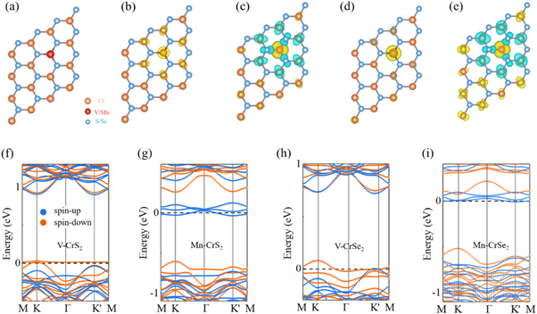
Figure 3. (a) Crystal structure of V/Mn-doped monolayer CrX2. Spin-density distributions of (b) V- and (c) Mn-doped monolayer CrS2. Spin density distributions of (d) V- and (e) Mn-doped monolayer CrSe2. The yellow and green isosurfaces in (b)–(e) correspond to the spin-up and spin-down states, respectively. Band structures of (f) V- and (g) Mn-doped monolayer CrS2. Band structures of (h) V- and (i) Mn-doped monolayer CrSe2. The blue and orange lines denote spin-up and spin-down states, respectively. The Fermi level is set to 0 eV.
Download figure:
Standard image High-resolution imageThe band structures of V/Mn-doped CrX2 are shown in figure 3. Since the time-reversal symmetry is broken, the energy degeneracy between two valleys of V/Mn-doped CrX2 is expected to be lifted, i.e. E↓ (K) ≠ E↑ (K'). As shown in figure 3, for all cases, the top valence band at the K point is higher than that at the K' point. Therefore, the valley polarization is also achieved in monolayer CrX2 by magnetic doping of V/Mn. The valley polarizations for V/Mn-doped CrS2 (CrSe2) are as large as 40.4/65.8 (82.4/83.3) meV, significantly larger than that of tiny value generated by application of an external magnetic field (∼0.10 to 0.24 meV T−1) [29–32].
As shown in figure 3(f), there is a defect state locating closely to valence bands of V-doped CrS2, which would deform the valleys in the valence bands. But fortunately, the valleys in the conduction bands lie far away from the defect state. While for Mn-doped CrS2, although several defect states exist in the band gap, they lie far away from both the valance and conduction bands (see figure 3(g)). Considering the fact that the Fermi level crosses the bottom of the defect states, the valleys in the valance bands of Mn-doped CrS2 are more favorable. A similar case is also observed in Mn-doped CrSe2, in which the valleys in the conduction bands are deformed and the valleys in the valence bands are preserved; see figure 3(i). Compared with these three systems, the case of V-doped CrSe2 is more excellent. As shown in figure 3(h), for V-doped CrSe2, no impurity bands are introduced into band gap and the energy valleys are preserved well, which are ideal for practical application in valleytronic devices.
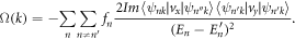
Because of the inversion symmetry breaking, the charge carriers in the K and K' valleys of monolayer CrX2 get a nonzero Berry curvature along the out-of-plane direction, which is the basis for realizing the valleytronics [2]. We then take I-CrS2/CrCl3 and V-doped CrS2 as examples to inspect the effect of magnetic proximity coupling and doping on the Berry curvature of monolayer CrX2. The Berry curvatures are derived from the Kudo formula [62], which can be expressed as:
Here, fn,  and νx/y are the Fermi–Dirac distribution function, the Bloch wave function with eigenvalue En, and the velocity operator along x/y directions. The corresponding Berry curvatures as a contour map in the 2D Brillouin zone are displayed in figures 4(a)–(c). For monolayer CrS2, as shown in figure 4(a), Ω(k) at the K and K' valleys are sizeable and exhibit opposite signs. While for I-CrS2/CrCl3 and V-doped CrS2, although the values of Ω(k) are slightly changed, they are still sizeable and feature opposite signs at the K and K' valleys (figures 4(b) and (c)). This firmly confirms that the particular features of Berry curvature are preserved in I-CrS2/CrCl3 and V-doped CrS2. The band structures of monolayer CrS2, I-CrS2/CrCl3 and V-doped CrS2 fitted by Wannier functions are shown in figure S5, which are in well agreement with DFT results.

Figure 4. Contour maps of Berry curvatures of (a) monolayer CrS2, (b) I-CrS2/CrCl3 and (c) V-doped CrS2. (d) Illustration of valley Hall effect in monolayer CrX2 with hole doping. (e) Illustration of anomalous valley Hall effect in valley polarized monolayer CrX2 with hole doping. The red and blue '+' in (d) and (e) represent the holes in K and K' valleys, respectively. The blue and red arrows in (d) and (e) depict the spin directions of carriers.
Download figure:
Standard image High-resolution image
Owning to the sign change of Berry curvatures in different valleys, the intriguing valley-contrasting physics is expected to be observed in monolayer CrX2. Namely, in the presence of a longitudinal external electric field, carriers located in opposite valleys will achieve opposite transverse velocities related to driving force of Ω(k) [9, 18]. For pristine monolayer CrX2 with hole doping, the holes in the K and K' valleys move to opposite directions of the sample under an in-plane electric field (see figure 4(d)), giving rise to the spin/valley Hall effect. While for CrX2/CrCl3 and V/Mn-doped CrX2, when hole doping them to shift the Fermi level between the K and K' valleys, namely the spin polarization is 100%, as shown in figure 4(e), spin-down holes from the K valley will move to the bottom of the sample under an in-plane electric field. The accumulated holes will result in a net charge/spin/valley current in the transverse direction [18]. Therefore, the intriguing anomalous charge/spin/valley effect is achieved in monolayer CrX2. We wish to emphasize that the accompanied anomalous charge/spin effect provide a measurable voltage for the anomalous valley effect. Moreover, when we reverse the magnetization direction of CrX2/CrCl3 and V/Mn-doped CrX2 by an external magnetic field, spin-up holes from the K' valley will move to the top of the sample under an in-plane electric field, leading a net charge/spin/valley current with opposite direction. It will also result in a measurable voltage but with opposite sign.
Conclusion
In conclusion, using first-principles calculation, we identify monolayer CrX2 as a promising 2D valleytronic material. We find that monolayer CrX2 is a direct-gap semiconductor. It exhibits two inequivalent valleys at the K and K' points and shows a very large valley spin splitting in the valence band. We further propose proximity coupling with monolayer CrCl3 to realize the long-sought valley polarization in monolayer CrX2. And the valley polarization in CrX2/CrCl3 can be engineered by the stacking pattern. Moreover, we reveal utilizing V and Mn doping can also leads to valley polarization in monolayer CrX2. Specially for the case of V-doped monolayer CrSe2, no defect state appears in the band gap, which is beneficial for practical applications. Our works not only highlight an exceptional 2D valleytronic crystals but also provide promising ways for realizing valley polarizations in them.
Acknowledgments
This work is supported by the National Natural Science Foundation of China (No. 11804190), Shandong Provincial Natural Science Foundation of China (Nos. ZR2019QA011 and ZR2019MEM013), Qilu Young Scholar Program of Shandong University, and Taishan Scholar Program of Shandong Province, and Youth Science and Technology Talents Enrollment Project of Shandong Province (No. 2019RKE27004).
Notes
The authors declare no competing financial interest.