


Abstract
The form of the external potential (FEP) for generating field emission resonance (FER) in a scanning tunneling microscopy (STM) junction is usually assumed to be triangular. We demonstrate that this assumption can be examined using a plot that can characterize FEP. The plot is FER energies versus the corresponding distances between the tip and sample. Through this energy–distance relationship, we discover that the FEP is nearly triangular for a blunt STM tip. However, the assumption of a triangular potential form is invalid for a sharp tip. The disparity becomes more severe as the tip is sharper. We demonstrate that the energy–distance plot can be exploited to determine the barrier width in field emission and estimate the effective sharpness of an STM tip. Because FERs were observed on Pb islands grown on the Cu(111) surface in this study, determination of the tip sharpness enabled the derivation of the subtle expansion deformation of Pb islands due to electrostatic force in the STM junction.
Export citation and abstract BibTeX RIS

Original content from this work may be used under the terms of the Creative Commons Attribution 3.0 licence. Any further distribution of this work must maintain attribution to the author(s) and the title of the work, journal citation and DOI.
1. Introduction
Field emission is a phenomenon that electrons are emitted from the conductor under the influence of an external electric filed. In a field emission experiment, the distance between the metal and the ground is typically in the range of micrometers to millimeter, and the emission current simply increases with the negative bias voltage. However, when the distance is reduced to the nanometer scale and under the configuration of the scanning tunneling microscopy (STM), electrons in the tunneling gap can form standing waves with quantized energies. Under this condition, the differential field emission current becomes oscillatory with the applied voltage. This quantum phenomenon is termed the field emission resonance (FER), which was theoretically predicted by Gundlach in 1966 [1].
Since Binning et al and Becker et al observed FER using STM [2, 3], FER has been a powerful technique widely exploited to investigate the surface reconstructions [4, 5] and properties [6], the atomic structure of the insulator surface [7], local work functions [8–12], the resistance at the nanometer scale [13], as well as the dynamics [14, 15] and lateral quantization [16, 17] of surface electrons above the vacuum level. Our recent studies have demonstrated that the field enhancement factor and sharpness of an STM tip can be qualitatively identified by counting the number of FERs [18, 19]. Higher sharpness is manifested by a larger number of FERs.
In an STM junction, the form of the external potential (FEP) that generates FERs was assumed in previous studies to be triangular [9, 10, 12, 13, 18]. This assumption implies that the structures of the tip and sample are parallel plates. In reality, however, the structure of an STM tip is widely accepted to be a base with a typical radius of several hundred angstroms on which a tiny protrusion is mounted. The tiny protrusion is why STM has atomic resolution, and electrons in FER are emitted from it. Therefore, the FEP is not necessarily triangular. Nevertheless, unless FEP can be experimentally observed, researchers have no choice other than to assume a triangular potential for the FER.
In this study, FERs were observed on Pb islands that were grown on Cu(111) surface and contained quantum well (QW) states [20–26]. We demonstrate that FEP can be observed by plotting FER energies versus the corresponding distances between the tip and sample. We discover that the energy–distance plot is nearly linear for a blunt STM tip. However, the energy–distance plot becomes more nonlinear as the tip sharpness increases. We demonstrate how this energy–distance plot can be exploited to acquire physical quantities not previously accessible. For instance, the width of the energy barrier in field emission can be extracted from the fitting of FER energies using the method of WKB approximation with obtained FEP. By modeling the tiny protrusion as a cone, the effective sharpness of a tip, which is the open angle of the cone, can be estimated through the calculation of the electric potential that fits the barrier width. Moreover, we demonstrate that the calculations including the known tip's effective sharpness, Pb band structure, and the WKB approximation enabled us to measure the subtle expansion of Pb islands [27] resulting from the electrostatic force in an STM junction.
2. Experimental details
In the experiment, clean Cu(111) surface was prepared using ion sputtering followed by annealing at 600 °C in cycles. To create flat Pb islands, Pb was evaporated onto the Cu substrate at 300 K with a flux of 0.03 monolayer per minute using an effusion evaporator. FERs were observed using an ultra-high vacuum STM operated at 4.3 K. Differential I–V spectra under the closed-loop condition were acquired by combining Z–V spectroscopy with the lock-in technique of adding a dither voltage of 45 mV at a frequency of 3.3 kHz to the bias voltage.
3. Results and discussion
3.1. Energy-distance plot
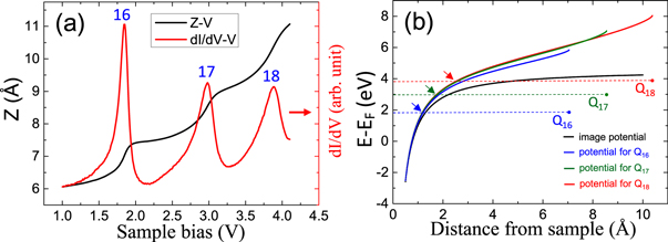
Figure 1(a) displays a typical STM topography image of Pb islands grown on Cu(111) surface. All of spectra observing FERs were acquired for islands with thickness of nine atomic layers under a current of 1 nA for energy ranging from 0.5 to 10 eV above the Fermi level. Because of the wide energy range, the QW states and FERs appeared simultaneously, but only the spectra of states above vacuum level (4.6 eV from Fermi level) are presented. Figure 1(b) displays a differential I–V spectrum with five FER peaks and its corresponding Z–V spectrum. Because a Z–V spectrum contains information about the distance between the tip and sample (named tip-sample distance hereafter), five tip-sample distances corresponding to five FER energies can be obtained. For measuring the tip-sample distance at 0.5 V, firstly, we used Z–V spectroscopy to measure the distance change by reducing the bias voltage from 0.5 V to 1.0 mV under 1 nA. Afterward, the feedback loop was turned off, and the tip was moved to approach the surface under 1.0 mV to observe the current increase. Once the current versus the distance of moving tip started to deviate from the exponential relationship, which is usually defined as the contact of the tip and sample, the distance change in this step was determined. Therefore, the tip-sample distance at 0.5 V was measured to be the summation of these two distance changes, which is 4.5 ± 0.2 Å.
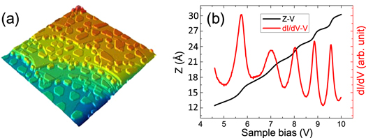
Figure 1. (a) Three-dimensional STM image of flat Pb islands on Cu(111) acquired under 0.5 V and 1 nA. The image size is 360 × 360 nm2. (b) Differential I–V spectrum with five FER peaks and its corresponding Z–V spectrum.
Download figure:
Standard image High-resolution imageWe plotted resonance energy (E) versus tip-sample distance (D) (figure 2(a)) by connecting data points (squares) with lines. This E–D plot reveals that the energy is almost linearly proportional to the distance, which indicates the accuracy of the triangular potential model wherein the quantized state energy is linearly proportional to distance, as illustrated in figure 2(b). Conversely, figure 2(b) also indicates that the potential can be depicted if the quantized state energies and their homologous distances are known. On the basis of this elucidation, the E–D plot in figure 2(a) can be interpreted as the FEP that results in FER in an STM junction. Therefore, the triangular potential model is valid for the description of the five FER peaks in figure 1(b).
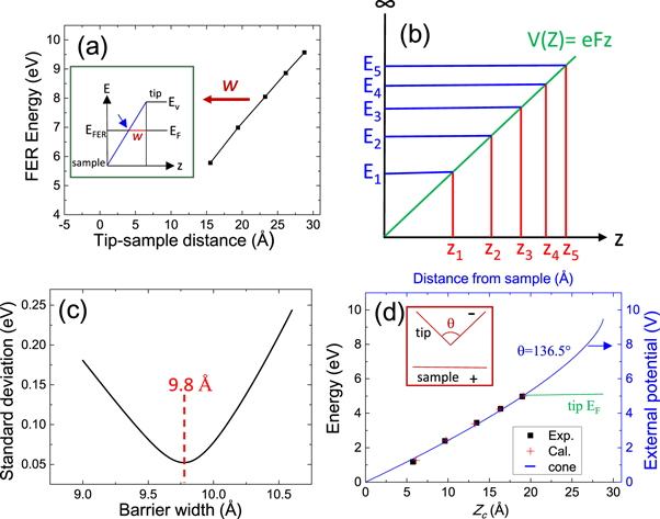
Figure 2. (a) Plot of FER energy (E) versus tip-sample distance (D). The plot is displaced (marked by an arrow) a length equal to the barrier width w along D axis. Inset: schematic of indicating the barrier width w and the classical turning point (marked by an arrow) in a triangular potential. (b) Schematic of the triangular potential model wherein the quantized state energy is linearly proportional to the distance. (c) Standard deviation of differences between calculated and measured FER energies as a function of w has a minimum corresponding a barrier width of 9.8 Å. (d) E–D plot in (b) is displaced 9.8 Å to be a diagram (squares) of experimental FER energy versus the distance Zc from the sample to the classical turning point, which is compared with another diagram (crosses) of calculated energy versus calculated Zc for the local minimum in (c). The energy axis here is relative to the vacuum level of sample. Inset: STM tip modeled as a conical shape with an open angle θ for calculating the external potential. The curve is an external potential calculated under θ = 136.5°, sample bias voltage = 9.5 V and tip-sample distance = 28.8 Å that can be known from FER of the highest energy. The barrier width in this calculated external potential is 9.8 Å, indicated by the length of the line representing Fermi level of the tip.
Download figure:
Standard image High-resolution imageBecause most of the field emission current comes from electrons near the Fermi level of the tip, the field emission current depends on the shape of the potential above the Fermi level (up to vacuum level). When FER occurs, electrons at the Fermi level of the tip must penetrate the energy barrier with a width w into the vacuum to couple into a quantized state, as illustrated by the triangular potential model in the inset in figure 2(a). The region in which electrons can form a standing wave in the vacuum is the tip-sample distance corresponding the quantized state minus the width of the energy barrier, i.e. the distance Zc from the sample to the classical turning point indicated by an arrow in the inset. The barrier width is basically determined by the shape of the potential above the Fermi level. Because the potential shape of this part is governed by the structure of the tip apex, the energy barrier is insensitive to the tip-sample distance. Consequently, we can assume that the barrier width was the same for all resonances in figure 1(b). As a result, the FEP depicted in figure 2(a) must be displaced for a length equal to a barrier width w along D axis to become the external potential, as indicated in figure 2(a). Hence, the determination of FEP also enables the measurement of the barrier width in field emission. Unfortunately, the E–D plot presented in figure 2(a) does not contain the potential form between the vacuum level and the lowest energy FER peak, which is necessary for acquiring the barrier width. Thus, after displacing FEP, a linear potential is introduced to connect these two energy levels. Subsequently, the assumed external potential dependent on w can be determined.
We next used the WKB approximation [28] to calculate the energies of quantized states in the assumed external potential ϕ(z) for different barrier widths, i.e.

where n is the quantum number, En is the energy of quantized state of quantum number n, z is the distance from sample. The standard deviation of differences between calculated and measured FER energies for each w was calculated. Figure 2(c) displays the standard deviation as a function of w, which has a minimum. We suggest that the barrier width is determined from this minimum, which is 9.8 Å. The E–D plot in figure 2(a) is thus displaced 9.8 Å to be a diagram of experimental FER energies versus Zcs shown in figure 2(d) (squares). This diagram is consistent with the calculated diagram (crosses) that is quantized state energies versus Zcs for the local minimum in figure 2(c), implying the validity of barrier width of 9.8 Å.
3.2. Effective sharpness of STM tip
In our experiment, the tip was made of poly-crystalline tungsten, which has a work function of 4.5 eV. The strength of the electric field of field emission can be estimated to be at least 4.5 V/9.8 Å = 0.46 V/Å. On the other hand, from the slope of the FEP in figure 2(b), it can be known that the electric field strength of the FERs is 0.29 V/Å. Consequently, the electric field of the field emission is stronger than that of FERs, which can be attributed to the sharpness of the STM tip that enhances the electric field near the tip but weakens that near the sample [19]. This situation is unable to be explained by the model in the inset in figure 2(a) where the STM tip is a plane. The structure of an actual STM tip is a base with a typical radius of several hundred angstroms on which an atomic-size protrusion is mounted. The protrusion is why STM has atomic resolution. Field emission current is emitted from the protrusion, leading to the mapping of high spatial resolution using FER [4, 5, 18]. In this work, the protrusion was modeled as a cone, as illustrated in the inset of figure 2(d). With this model, the sharpness of an STM tip can be quantitatively represented by an effective sharpness that is an open angle θ of the cone, and then the external potential can be calculated [29]. We demonstrate herein that the effective sharpness can be estimated by calculating the external potential that fits the obtained barrier width.
In the calculation, the external potential ϕcal in the direction normal to the sample follows

where Aν is a constant, Zts is the tip-sample distance, and z is the distance from the sample. By solving Legendre polynomials Pν under the condition of Pν (π − θ/2) = 0, a series of positive ν can be obtained. Because the tip-sample distance is much smaller than the size of the tip, only the smallest ν is considered. Equation (2) is thus reduced to be

Because w and the work function of the tip Wtip are known, Aν can be obtained from

and Aν should satisfy

where Vbias is the applied bias voltage, and Wsample is the work function of the sample (4.6 eV).
The curve in figure 2(d) is the external potential calculated using cone model for the FER of the highest energy. To calculate this potential, θ was taken as 136.5°, and the barrier width in this potential was exactly 9.8 Å, as indicated by the length of the line representing the Fermi level of the tip. Therefore, the effective sharpness of the tip for five FERs in figure 1(b) was 136.5°. Moreover, the part of the curve in figure 2(d) below the Fermi level of the tip is a favorable fit for all of the FER energies, indicating that the calculated external potential in this region is nearly linear. This is why the triangular potential model was deemed valid in previous studies and consideration of tip sharpness was unnecessary.
Figures 3(a) and (b) display differential I–V spectra with six and nine FERs, respectively, and their corresponding Z–V spectra. Figures 3(c) and (d) depict the E–D plots established from figures 3(a) and (b), respectively. Unlike the FEP depicted in figure 2(a), the FEP presented in figure 3(c) is nonlinear; this is even more evident in the FEP presented in figure 3(d). Therefore, the triangular potential model is invalid when more FERs occur. The nonlinear feature can be attributed to the spherical base of STM tip. Owing to the spherical base, the electric field generating FERs decays with the tip-sample distance, resulting in a nonlinear FEP. Hence, the enhancement in the nonlinearity of the FEP with an increase in the number of FERs can be attributed to a reduction in the base radius. We used the same procedures as previously to calculate the standard deviation as a function of barrier width for these two FEPs in figures 4(a) and (b). The standard deviation curves again have minimum, allowing us to determine that the barrier width is 9.2 Å for the six resonances and 8.0 Å for the nine resonances. In figures 4(c) and (d), the calculated diagrams (crosses) are in close agreement with the experimental diagrams (squares) of the six and nine resonances. The curves presented in figures 4(c) and (d) are the calculated external potentials that fit the barrier widths obtained from figures 4(a) and (b), respectively. Thus, we know that the effective sharpness is 121.1° for the six resonances in figure 3(a) and 84.6° for the nine resonances in figure 3(b). Evidently, a larger number of FERs corresponds to higher effective sharpness, which is consistent with the results of our previous study [19].
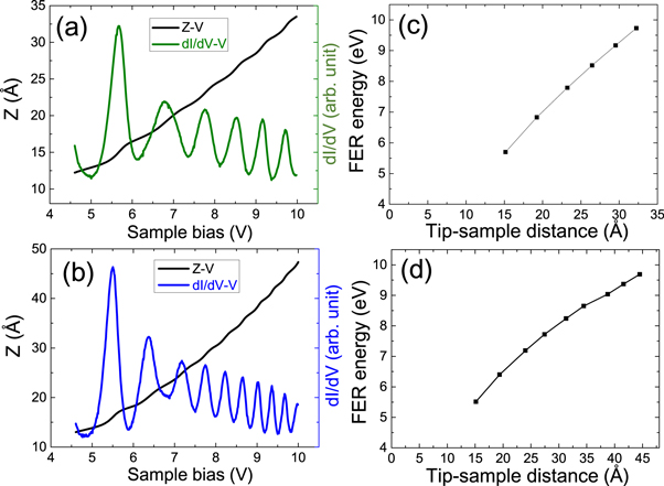
Figure 3. (a) Differential I–V spectrum with six FERs and its corresponding Z–V spectrum. (b) Differential I–V spectrum with nine FERs and its corresponding Z–V spectrum. (c) E–D plot established from (a). (d) E–D plot established from (b).
Download figure:
Standard image High-resolution image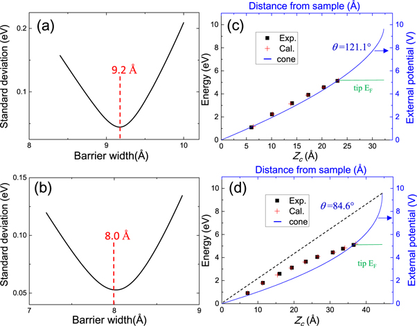
Figure 4. (a) Standard deviation as a function of barrier width (w) derived from E–D plot in figure 3(c), with a minimum at w = 9.2 Å. (b) Standard deviation as a function of w derived from E–D plot in figure 3(d), with a minimum at w = 8.0 Å. (c) Calculated diagram (crosses) and experimental diagram (squares) when w = 9.2 Å. The curve is an external potential that fits w = 9.2 Å, calculated under θ = 121.1°, and sample bias voltage = 9.63 V and tip-sample distance = 32.3 Å that can be known from FER of the highest energy. (d) Calculated diagram (crosses) and experimental diagram (squares) when w = 8.0 Å. The curve is an external potential that fits w = 8.0 Å, calculated under θ = 84.6°, and sample bias voltage = 9.59 V and tip-sample distance = 44.5 Å that can be known from FER of the highest energy. The dashed line indicates the linear potential due to the planar tip.
Download figure:
Standard image High-resolution imageThe FEP and barrier width are independent of the work function of the tip. But the estimated effective sharpness may indeed change with the work function of the tip. Actually the work function of tungsten is in a range of 4.3–5.25 eV because of various surface orientations [30, 31]. Therefore, we also estimate the effective sharpness (cone angle) under work functions of 4.3 and 5.25 eV for five, six, and nine FERs. The results reveal that the cone angle decreases with increasing the work function monotonically for all three cases (not shown). For the work function varying from 4.3 to 5.25 eV, the angle change is 140°–122° for five FERs, 124°–107° for six FERs, and 88°–72° for nine FERs. Because the angle uncertainties of three cases are only about 17°, even the work functions of the tungsten tips for generating five, six, and nine FERs are all different, the tip sharpness can still be identified by the number of FERs.
Unlike in figure 2(d), the calculated external potential below Fermi level of the tip in figure 4(c) obviously deviates from the FEP for six FERs, and figure 4(d) demonstrates that this deviation is larger in the case of nine FERs. In figure 4(d), a linear potential (dashed line) due to a planar tip is added to compare to the FEP and calculated external potential. It can be seen that the linear potential is above the calculated external potential, and the FEP is between them. Therefore, the potentials due to planar and conical tips are two extremes. The potential due to the tip consisting of a spherical base and a cone-like protrusion should be between these two extremes. Owing to that the nonlinear FEP in this case is associated with the base radius, the deviation can be attributed to the influence of the base. Because the electric field in FERs is always much weaker than that in field emission, the effect of the base structure on the electric field of the field emission can be ignored. Accordingly, the cone model is appropriate for estimating the effective sharpness of the protrusion, but it cannot describe the external potential caused by a sharp tip.
A shorter barrier width was further discovered to be associated with higher effective sharpness. If the same field emission current is used to acquire spectra, a shorter barrier width should correspond to a larger energy barrier height. Therefore, we infer that a sharper tip has a larger barrier height. The energy barrier results from the superposition of the external potential and the image potential near the tip, and its height is determined by the work function of the tip. Because the work function is independent of tip sharpness, the variation in the barrier height with sharpness indicates that the image potential is likely sharpness-dependent. According to electrostatics, the image potential at a given distance from a cone is lower than that at the same distance from a plane. Thus, the image potential from a cone must decrease as the open angle is reduced, implying that the image potential effect is weaker for a sharper tip. The barrier height thus increases when the external potential superposes on a weaker image potential, explaining why a sharper tip corresponds to a larger barrier height.
3.3. Field effect on the width of confining well
Although previous studies have demonstrated that electrostatic force in an STM junction can induce the expansion deformation in Pb islands, this expansion has not yet been quantified. In this study, we demonstrate that the expansion can be quantitatively measured. Under the electric field, the quantized condition for a QW state with a wavevector k in Pb islands on Cu(111) is [27]

where N is the number of atomic layer in islands, d is the interlayer spacing, n' is the quantum number, Δt is the size of the expansion, and ϕB' is the phase associated with the potential in the vacuum, which is the superposition of external potential and image potential near the sample.
We suggest here that k can be directly determined from the measured energy E of the QW state through the band structure of Pb in Γ–L direction (an E–k dispersion) [32]. Hence, using equation (2), Δt can be obtained if ϕB' is known. ϕB' can be acquired by calculating the electronic phase in the potential in the vacuum using the WKB approximation—for which, however, the external potential must be known. We have demonstrated that only the external potential caused by a blunt tip is well described by the cone model (figure 2(d)). Therefore, in the following, the cone model with effective sharpness 136.5° and the differential I–V spectrum with QW states and its corresponding Z–V spectrum (figure 5(a))—which were acquired by the same tip for five FERs in figure 1(b)—are used to extract Δt. The numbers indicated above the three QW state peaks in figure 5(a) are quantum numbers. For each QW state, the potential difference and distance between the tip and sample can be known from the QW state energy and Z–V spectrum, respectively. Accordingly, we can depict the external potential using the cone model, and superpose it with the image potential to define the potential in vacuum, as shown in figure 4(b). ϕB' for each QW state is thus calculated with the WKB approximation, that is,

where Qn' is the energy of a QW state, ϕ'(z) is the potential in the vacuum. Finally, Δt is determined by substituting the obtained k and ϕB' into equation (6). The results reveal that under a current of 1 nA, the expansion in Pb islands with thickness of nine atomic layers is 0.9, 0.9, and 1.0 Å when the bias voltages are 1.85, 2.98, and 3.88 V, respectively. Because Z–V spectroscopy is used, the distance between the tip and sample increases with increasing the bias voltage. As a result, the electric field and the electrostatic force in STM junction are nearly unchanged when the bias voltage is ramped. Accordingly, the expansion is insensitive to the bias voltage.
Figure 5. (a) Differential I–V spectrum showing three QW states and its corresponding Z–V spectrum. The numbers above QW state peaks are quantum numbers. (b) Energy diagrams of image potential near the sample superposed with the external potential, used to calculate the electronic phases in vacuum in three QW states through the WKB approximation. The image potential near the tip is ignored. Dots indicate the positions of the tip. The dashed line indicates the energy Qn' of QW state of quantum number n'. Arrows indicate the classical turning points.
Download figure:
Standard image High-resolution image
4. Conclusion
In summary, we demonstrate that the E–D plot constructed from FERs and the Z–V spectrum contains valuable information. This simple plot can be used to characterize the FEP of FERs, and acquire knowledge about the STM tip such as its barrier width for field emission and effective sharpness. With this knowledge, we can further measure the field-induced expansion deformation of Pb islands on the Cu(111) surface. Therefore, the E–D plot is useful for understanding the field-induced phenomena observed using STM.
Acknowledgments
This work was supported by the Ministry of Science and Technology (grant No.: MOST 103-2112-M-001-022-MY3) and Academia Sinica (Thematic Project, grant No.: AS-105-TP-A03), Taiwan.