


Abstract
Using shallow implantation of ions and molecules with masses centred at 27 atomic mass units (amu) in diamond, a new artificial optical centre with unique properties has been created. The centre shows a linearly polarised fluorescence with a main narrow emission line mostly found at 582 nm, together with a weak vibronic sideband at room temperature. The fluorescence lifetime is ∼2 ns and the brightest centres are more than three times brighter than the nitrogen-vacancy centres. A majority of the centres shows stable fluorescence whereas some others present a blinking behaviour, at faster or slower rates. Furthermore, a second kind of optical centre has been simultaneously created in the same diamond sample, within the same ion implantation run. This centre has a narrow zero-phonon line (ZPL) at ∼546 nm and a broad phonon sideband at room temperature. Interestingly, optically detected magnetic resonance (ODMR) has been measured on several single 546 nm centres and two resonance peaks are found at 0.99 and 1.27 GHz. In view of their very similar ODMR and optical spectra, the 546 nm centre is likely to coincide with the ST1 centre, reported once (with a ZPL at 550 nm), but of still unknown nature. These new kinds of centres are promising for quantum information processing, sub-diffraction optical imaging or use as single-photon sources.
Export citation and abstract BibTeX RIS

Original content from this work may be used under the terms of the Creative Commons Attribution 3.0 licence. Any further distribution of this work must maintain attribution to the author(s) and the title of the work, journal citation and DOI.
1. Introduction
Defect centres in diamond are getting more and more into focus for a large range of application in physics, material science and bio-technology. Diamond material and defects are especially well suited for solid-state quantum information processing and quantum sensing at room temperature [1–5]. The wide transparency range of diamond and the large amount of optically active defect centres also offer the possibility to engineer single-photon sources operating at room temperature [6–11]. The optical properties of such non-classical light emitters can furthermore be controlled or improved by use of adequate photonic structures [12–16]. For biomedical applications, fluorescent nano-diamonds containing nitrogen-vacancy (NV) centres are widely used for imaging and future therapy schemes [17, 18]. Furthermore, the unique spin and optical properties of the NV centres in diamond have led to single molecule NMR [19–21]. The main important features of the NV centre that enable these kinds of applications are the optical readout and coherent control of single spins with extremely long coherence time at room temperature [22, 23]. Among hundreds of defect centres known in diamond, these exceptional properties have been found up to now only for the NV centre and the ST1 centre [24]. Recently, the feasibility of all-optical control of the SiV spins at 4 K using ultrafast laser pulses has been reported [25]. Whereas the NV and the SiV centres can be produced in a controlled way using ion beam implantation or diamond growth [26–29], the ST1 centre was found once in a surface etched high-pressure, high temperature (HPHT) diamond [24] and could not be reproduced up to now. Despite its prosperousness, the NV centre has some disadvantages. It is formed after annealing and involves a carbon vacancy, therefore a deterministic fabrication by ion implantation is highly challenging [27] (the same creation efficiency far from 100% applies also to the SiV centre which involves two carbon vacancies). Additionally, the NV centre shows a very large phonon coupling. This leads to a broad emission spectrum, thus coherent coupling schemes using photons are hardly achievable with NV centres. The SiV centre however possesses a narrow emission and weak phonon coupling which enable quantum protocols with indistinguishable photons [30].
Ion implantation addresses single atoms and defects with high spatial resolution in three dimensions. Using this method, the production of an entangled quantum register and quantum sensors at room temperature has already been demonstrated using NV centres [2]. Due to the extremely small diffusion constant in diamond, atoms placed by ion implantation remain at the same crystal position even after high temperature treatments. This stability reduces bleaching effects or formation change due to laser irradiation.
We report here the formation of a new defect centre, with narrow fluorescence (FWHM <1.4 nm), emitting mostly at 582 nm (hereafter termed the L1 centre). This L1 centre was created by ion implantation technique and, to our knowledge, was not found in any natural, synthetic or processed diamond before. Its spectral properties as well as its polarisation and blinking behaviour are studied in detail in section 3.1. Additionally, another kind of optical centre has been created within the same sample and ion implantation run, with a zero-phonon line (ZPL) emitting at ∼546 nm and showing electron spin resonance. As discussed in section 3.2, this hereafter termed L2 centre probably coincides with the already reported ST1 centre.
2. Experimental details
Two ultrapure highly polished (001)-oriented single crystal CVD diamonds (Element Six Ltd, electronic grade) with residual concentration of nitrogen below 5 ppb have been used for this study. The samples have been preliminary cleaned using an oxygen plasma treatment (180 W, 0.4 mbar). Before implantation, a few areas of the selected side of the diamond have been controlled by confocal microscopy. No optical centres could be observed in the spectral window 550–850 nm. The ion implantation was then performed using the 100 kV accelerator at the University of Leipzig, producing a beam of negatively charged ions. The home-built accelerator is equipped with a commercial cesium sputter source which allows to implant nearly all kinds of ions. For this study, the cathode was filled with a mixture of graphite and boron nitride. The ion implantation was performed at the energy of 52 keV and a 90° bending magnet was adjusted to select the ion masses from a broad peak centered at 27 amu (expected to correspond to CN− ions) intending to produce NV centres. The ion fluence was chosen to be 1 × 1010 cm−2. A thermal annealing was further performed for both samples, at 800 °C in vacuum for 2 h.
The optical characterisations were done using a home-built scanning confocal fluorescence microscope equipped with a 532 nm frequency-doubled Nd:YAG laser for the excitation, focused to the sample with a high numerical-aperture objective (Olympus, ×100, NA = 0.95, air). The same objective collects the fluorescence which is separated from the laser reflection by a dichroic mirror and interference filters. A 50/50 beamsplitter is further used to send half of the signal towards two single-photon counting modules built in a Hanbury-Brown and Twiss configuration (for imaging and correlation measurements) and the other half towards a cooled CCD spectrometer.
For the optically detected magnetic resonance (ODMR) measurements, the sample was fixed on a printed circuit board between the ends of two coplanar waveguides with ground-plane [31]. A copper wire of 20 μm diameter was placed in the middle of the sample and soldered to the two ends of the waveguide. One end was terminated with a 50 Ω load and the other was connected to the microwave source to which a MW field of ∼6 dBm intensity was coupled into the wire while performing the frequency sweep for the ODMR. All the experiments were performed at room temperature.
3. Results and discussion
The L1 centres and the L2 centres were found simultaneously and on both samples. Figure 1 is a confocal fluorescence scan of the implanted surface of sample 1. At first sight, it can be seen that there is a density of fluorescing centres of about 1 × 108 cm−2. With respect to the ion fluence of 1 × 1010 cm−2, this corresponds to a total creation yield of about 1%. This is, for comparison, slightly less than for the NV centres, nevertheless in the same order of magnitude [27]. Different kinds of centres can be observed. The continuous and dotted circles highlight a stable and a blinking L1 centre (described in section 3.1), respectively. The other centres are the L2 centres, described in section 3.2. The square indicates one of these centres. Note that no NV centres are found in this sample.

Figure 1. Confocal fluorescence scan of the first implanted diamond sample. The detection spectral window is 575–630 nm and the laser excitation wavelength is 532 nm. Different kinds of optical defects are found: centres having a narrow emission line around 582 nm (L1 centres) and centres with a ZPL around 546 nm along with a broad phonon sideband (L2 centres). The plain circle points out a stable L1 centre while the dotted circle points out a blinking one. The square indicates a L2 centre.
Download figure:
Standard image High-resolution image3.1. The L1 centre (582 nm)
The spectral properties of the L1 centres are firstly described in the following. Figure 2(a) shows the background corrected fluorescence of a typical L1 centre under 532 nm excitation at room temperature. The fluorescence spectrum has a very narrow emission line at 581.7 nm (2.134 eV). A weak and characteristic vibronic sideband is found, showing a broad peak around 600 nm together with some features between 640 and 650 nm (with energies of 196.4, 209.1 and 219.2 meV). The FWHM of the main 581.7 nm emission line was determined to be less than 1.4 nm. The resolution of the home-built spectrometer is in the order of 1 nm, thus the linewidth may be even narrower. Remarkably, about 55% of the intensity is found in the main emission line. The brightness of the L1 centres varies from one centre to the other. The brightest ones do reach emission rates of about 7 × 10⁵ counts s−1 at saturation (at about 3 mW with an objective with NA = 0.95), much higher than the NV centres. The saturation curve of a typical L1 centre is shown in figure 2(b). The single emitter nature of the defect is proved by the second-order photon autocorrelation function plotted in figure 2(c) which goes to zero at zero time delay. The g(2) function has been background corrected and normalised. From the fit of the dip, a lifetime of about 1.7 ns is estimated for the excited state. Furthermore, the bunching shoulders indicate the presence of a long-lived shelving state of about 700 ns. At this stage it is not possible to conclude whether the main emission line is the ZPL of the defect. The spectral study of several centres reveals a spread in the position of the emission line. This spread extends over more than 20 nm, between 577 and 605 nm, with a maximum at about 582 nm (figure 3(a)).
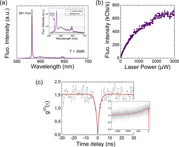
Figure 2. (a) Fluorescence spectrum of a single L1 centre at room temperature, with 532 nm excitation. The spectrum is background corrected. The inset shows, plotted in logarithmic scale, the raw spectrum of the same centre together with the background reference measurement (taken at the same depth and 1 μm apart from the L1 centre). (b) Background corrected saturation curve of a single L1 centre, measured without the 50/50 beamsplitter for spectrometry (the fluorescence intensity scale shows the full counts). (c) Photon autocorrelation function g(2)(τ) measured at a laser power of 750 μW. The curve is background corrected and normalised. The dip going to zero at zero time delay proves the single quantum emitter behaviour of the defect. The exponential fit gives a lifetime of 1.7 ns for the excited state. The inset shows the g(2) function for a longer time scale. The bunching shoulder reveals a long-lived shelving state of about 700 ns.
Download figure:
Standard image High-resolution image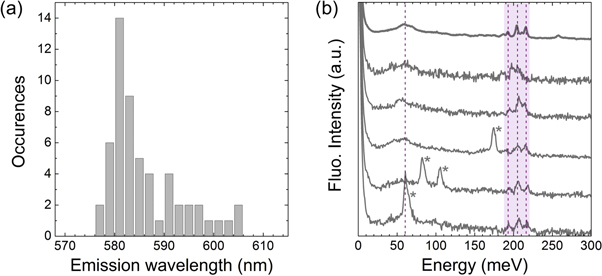
Figure 3. (a) Histogram of the observed positions of the emission lines of 56 L1 centres. (b) Sideband spectra of six of these centres. All spectra are background subtracted and normalised to the maximum of the emission line.
Download figure:
Standard image High-resolution imageIt is believed that this spread is due to stress or environmental changes and that all the centres observed here are of the same nature. Note that for SiV or Cr centres, the ZPL can shift for several nm due to the same reasons [32, 33]. A spread in the brightness of the centres is also observed, which can vary of about one order of magnitude. No correlation between the line position and the brightness of the centres could be found.
The vibronic sideband emission of the L1 centres is weak compared to the main emission line, even at room temperature, indicating a weak electron-phonon coupling. With respect to the spread of the emission line, the sidebands of several centres have been more precisely analysed. To this purpose, the sidebands have been plotted (in figure 3(b)) not in wavelength scale but as the energy difference with respect to the position of the main emission line (and normalised to its intensity). It can be seen at first sight that the sidebands of the L1 centres are similar. They all present a broad peak at about 60 meV (dotted line) as well as narrower features at higher energy, between 190 and 220 meV (shadowed area). These are attributed to local vibrational modes (LVM), since the phonon density of states has a sharp high-energy cutoff at 165 meV and decreases strongly below 70 meV [34].
A deeper analysis of these LVM may help understanding the structure of the L1 centre and what kind of atoms are involved. Furthermore, additional lines of higher intensity can be seen in the sideband region of some centres (indicated by the stars). At this stage it is not possible to conclude whether these features are electronic transitions or vibronic features. Further measurements at low temperature are required for clarification.
An additional property shared by all the L1 centres is a strong polarisation, measured both in absorption and in emission. For absorption measurements (figure 4(a)), a half-wave plate has been used to rotate the polarisation of the laser excitation, whereas a linear polarisation analyser has been placed in the detection path for the measurements in emission (not shown). Figure 4(a) shows the (background-corrected) polarisation diagrams in absorption of two typical L1 centres, representative of all the measured centres. The absorption maxima of a single centre are found either along the [110] direction or the [−110] direction. Similar polarisation diagrams are obtained in emission. It can further be seen that no absorption takes place for the polarisation perpendicular to the one of maximum absorption. The L1 centres behave therefore as single dipoles in absorption. A two-fold symmetry in the projected (001) plane is found and the fluorescence is maximum, or zero, along the 〈110〉 projected axes. No L1 centres having maxima along the [100] or the [010] directions could be found. The distribution of the directions of maximum absorption of more than 100 L1 centres is plotted in figure 4(b). This distribution indicates that the dipoles of the L1 centres are oriented along the 〈111〉 axes (figure 4(c)). If they would have been oriented along the 〈110〉 axes (as it will be seen later for the 546 nm centres), additional absorption maxima of lower intensity would have been found along the [100] and [010] directions, which is not the case. Moreover, the knowledge of the dipole orientation is of importance in what concerns the integration or coupling of single defect centres within photonic structures such as cavities or pillars. The narrow emission line at room temperature, the short lifetime, the brightness and the highly polarised emission are all important properties for the use of the L1 centre as a single-photon source. Although ZPL emission peaks have already been reported in the same spectral region as for the L1 centres, on the basis of the previously mentioned features and of the vibronic sideband this centre does not correspond to any known natural or artificial diamond defect line in the literature.

Figure 4. (a) Polarisation-dependent absorption of two representative single L1 centres. (b) Distribution of the projected direction of the absorption dipoles of a hundred L1 centres onto the (001) plane. (c) Projected 〈111〉 directions onto the (001) plane, showing the two possible orientations along the [110] and [−110] directions.
Download figure:
Standard image High-resolution imageBesides their high linear polarisation, several L1 centres show a blinking behaviour. Such centres, if integrated in nano-diamonds, are of interest as fluorescent markers for stochastic methods of super resolution microscopy techniques such as photo-activated localisation microscopy (PALM) [35] or stochastic optical reconstruction microscopy (STORM) [36]. In this view it is important to characterise the duty cycles and blinking dynamics of the centres. For a use in STORM/PALM techniques, the fluorescent markers need to be ON only a small period of time with respect to the time they are OFF. The sub-diffraction nanometer accuracy is obtained by reconstructing an overall image from a series of single images in which only a fraction of the centres is turned ON. In the scan of figure 1, four L1 centres having different blinking dynamics can be found. The fluorescence time trace of a chosen blinking single L1 centre (dotted circle) is recorded for different laser powers (from 200 to 1000 μW) for 2 min each, and plotted in figure 5(a). The higher the excitation, the faster the blinking of the L1 centre is driven.
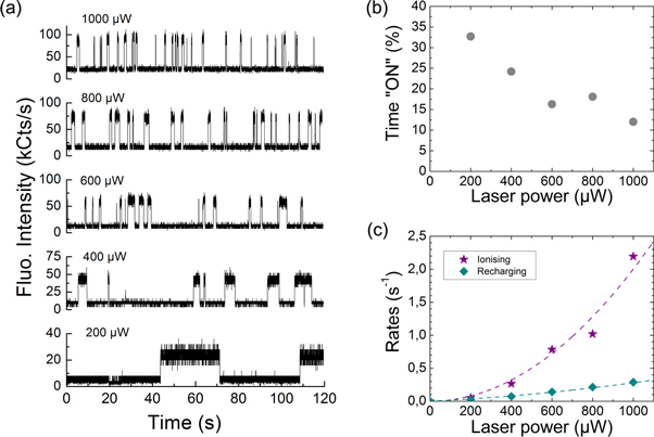
Figure 5. (a) Fluorescence time traces recorded for a blinking L1 centre at different excitation powers. (b) Duty cycle or probability for the L1 centre to be in the 'ON' state as a function of the laser power. (c) Power dependence of the ionising and recharging rates of the L1 centre.
Download figure:
Standard image High-resolution imageThe resulting durations of the ON and OFF states obtained from the time traces have then been sorted in a statistical distribution (not shown) and further fitted by Gaussian functions. Note that the intensity of the OFF state corresponds to the background fluorescence coming from the diamond. A threshold for the fluorescence intensity is then chosen to discriminate between the states in the trace. The distribution of the time spent in the bright ON state decreases exponentially, as well as for the time spent in the OFF state. As seen in figure 5(b), the bright to dark ratio (duty cycle) decreases as the laser power is increased. It is of advantage for STORM that the smallest duty cycle (about 10%) happens when the centres are the brightest. This would lead to smaller acquisition times for the single images and thus faster elaboration of the high-resolution reconstructed image. By analogy with previous work on NV-/0 photo-induced blinking of NV centres [37], the 'ionising' and 'recharging' rates of the L1 centre are plotted in figure 5(c), as a function of the laser power. Both curves are fitted using a second order polynomial function with fitting parameters found to be a = 0 and b = 2 × 10⁻⁶ for the ionisation rate curve, and a = 1.5 × 10⁻⁴ and b = 1.3 × 10⁻⁷ for the recharging rate curve. Both rates possess a term of quadratic increase with the laser power, characteristic of two-photon processes in the ionisation and recharging processes. The purely quadratic power dependence of the ionising rate suggests that the ground state of the L1 centre lies more than 2.13 eV below the conduction band, following a similar reasoning applied to NV centres in [37].
The cause of the blinking behaviour is not clear at this stage of the investigation. Possible explanations are a transition in a dark state or a change of the charge state. In some cases, the L1 centres become irreversibly dark, thus a change of the charge state is more likely. These behaviours are probably due to different local environments of the L1 centres, as it can also be observed for other optical centres in diamond such as the NV centre and the SiV centre [38]. Further investigations of the stability/blinking behaviour of the L1 centres are planned, when donor and/or acceptor atoms are co-implanted to the L1 centres. Finally, we have investigated whether the L1 centre is ESR active in the MW spectral ranges of NV and ST1 centres (0.94–1.04 GHz, 1.22–1.32 GHz and 2.82–2.92 GHz) but no resonances could be found in the optical fluorescence.
3.2. The L2 centre (546 nm) or ST1 centre
The second kind of centre which was found together with the L1 centre within the implanted samples is denoted here as the L2 centre. Note that, in the first sample, the L1 centres were found in majority (90%–95%) with respect to the L2 centres (5%–10%) whereas an opposite ratio was found in the second implanted sample. The L2 centre presents different properties than the L1 centre. Firstly, the fluorescence spectrum of a typical L2 centre is plotted in figure 6(a) (with background correction). It can be seen that, at room temperature, the emission consists of a narrow ZPL at 545.9 nm (2.274 eV) and of a broad phonon sideband extending up to 800 nm. The FWHM of the ZPL is 1.4 nm and about 2% of the light is emitted in the ZPL. The observation of several L2 centres revealed that the position of the ZPL is spread, in the range 540–547 nm. The brightness of the L2 centres is changing from one centre to the other and most of the L2 centres show a blinking behaviour, as illustrated in figure 6(b). The single emitter nature of the L2 centres is demonstrated by the g(2) function plotted in figure 6(c), taken at an excitation power of 200 μW. To fit these data, we assumed a three level model. From this approach, an excited state lifetime of about 9 ns has been extracted. At higher excitation power (1.66 mW) bunching shoulders appear (inset of figure 6(c)), revealing a long-lived shelving state of about 700 ns.
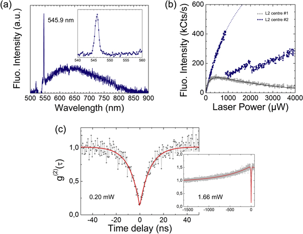
Figure 6. (a) Fluorescence spectrum at room temperature of a single L2 centre, with 532 nm excitation. The spectrum is background corrected. The dip around 532 nm is due to the notch filter used to preclude the laser reflection to enter the spectrometer. The inset shows the zero-phonon line. (b) Background-corrected saturation curves of two single L2 centres (with same optical and ODMR spectra) showing different behaviours. Most of the single L2 centres show a discontinuous saturation curve as the one of centre 2. (c) Photon autocorrelation function (at 200 μW laser power) showing the single quantum emitter behaviour of the L2 centre. The exponential fit gives a lifetime of ~9 ns for the excited state. The inset shows the g(2) function for a longer time scale at higher power (1.66 mW). The bunching shoulder reveals a long-lived shelving state of about 700 ns.
Download figure:
Standard image High-resolution imagePolarisation-dependent absorption measurements have also been realised with the L2 centres. Four different possible orientations are observed. The highest brightness is observed when the polarisation is along the 〈110〉 axes, while the lower brightness centres are observed for polarisation along the 〈100〉 axes. For symmetry reasons, it can therefore be deduced from these measurements that the absorption dipoles are oriented along the 〈110〉 axes. There are six equivalent positions for 〈110〉 oriented defects, which however reduce to four, as measured here, when projected onto the (001) plane.
The L2 centres were further subjected to continuous ODMR measurement schemes. This revealed two positive lines around 0.99 and 1.27 GHz with linewidths of 1–4 MHz (figure 7(a)). For these lines, contrasts of up to 6% and 20% were found, respectively. No intrinsic hyperfine splitting could be found, indicating that the atoms involved in the defect do not have a nuclear spin.

Figure 7. (a) Optically detected magnetic resonance (ODMR) spectrum of a single L2 centre at room temperature. (b) Decay curves from which the lifetimes of the spin triplet level can be extracted with a double exponential fit. (c) Tentative level scheme for the L2 centre. (d) Rabi oscillation on the indicated resonance frequency with either constant illumination (left) or pulsed light (right). The measurement scheme is similar to NV centres, but the initialisation laser pulse used was 7 μs long, and the two 250 ns counting windows were 5.5 μs apart to accommodate for the long shelving state lifetime.
Download figure:
Standard image High-resolution image
The kinetics of the shelving state observed in the second-order photon correlation function at high power has been investigated, with and without the employment of microwave π-pulses at 1.26 GHz. In the decay curves of the fluorescence (figure 7(b)), double exponential decays are observed, suggesting that the spin triplet is the shelving state, and not the ground state. A possible level scheme for this defect, with the corresponding measured lifetimes, is depicted in figure 7(c), as inspired from [24]. An additional presumed fourth level (dotted line) is however suggested here to cope with the discrepancy of the g(2) power sweep measurements (not shown) when a three level system is assumed. This additional level may furthermore account for the decrease of fluorescence when the excitation is increased (observed in the saturation curve, grey hollow circles in figure 6(b)).
The positive and relatively high contrast of the ODMR spectra is due to the longer lifetime (∼2500 ns) of the spin triplet sublevel  than the lifetime of the
  sublevel (∼700 ns) and of the
  sublevel (∼100 ns). This makes an optical pumping of the
  sublevel possible as well as a coherent manipulation of the associated spin. In the context of quantum technologies in the solid state based on the coupling between electron and nuclear spins, the spin-free ground state of the L2 centre is of advantage compared to the triplet ground state of the NV- centre, for which the presence of the electron spin causes decoherence to the nuclear spin. In the case of the L2 centre, the spin manipulation and readout can be achieved within the metastable excited spin state.
Rabi oscillations have then been performed to illustrate the coherent control between the triplet spin states; both between the  and
and  states (1.27 GHz) and between the
  and
and  states (0.99 GHz). Two schemes have been applied: with constant laser illumination (figure 7(d) left) and with pulsed light (figure 7(d) right). As seen in the two figures, the amplitude of the oscillations and the decay envelope can be well fitted using the model and time constants presented in figure 7(c).
The ODMR spectra of the L2 centres are very similar to the ones reported for the ST1 centre [24] (zero-field splitting parameters D = 1.135 GHz and E = 139 MHz) even if the ST1 centre shows a third resonance peak at 278 MHz. The optical spectra at room temperature are slightly shifted: the ZPL of the ST1 centre is at 550 nm and it is weaker than the one observed for the L2 centre. However, the ST1 and L2 centres show the same excited state lifetime of about 9 ns. The ST1 centre (the nature of which is still unknown) was found in an ultrapure single-crystal HPHT diamond, after the fabrication of nanowires [24]2 . The wires had been etched from the diamond surface by reactive ion etching using inductively coupled oxygen plasma. Afterwards, the sample had been annealed in vacuum at 850 °C for several hours. It was suggested by the authors that oxygen could be a potential constituent. Indeed, the ODMR measurements of single ST1 centres did not show any hyperfine coupling and 16O has no nuclear spin. In the case of the L2 centre observed in our sample, we also did not find any hyperfine coupling. It is therefore very likely that the L2 centre and the ST1 centre are the same defect, possibly with oxygen involved in it. The shift of the ZPLs may be explained by lattice deformation or by the presence of another impurity species.
Both the L1 and L2 centres have been created simultaneously twice, in two different samples, using the same implantation conditions and cathode source. It is important to note that only the implanted faces (front face of sample 1 and front and back faces of sample 2) show the presence of the L1 and L2 centres. No centre can be found on the unimplanted backface of sample 1, which excludes that the centres may have been induced solely by thermal annealing. However, the (probably) bi-atomic molecular ion used for implantation does not allow an unambiguous identification of their nature. The magnetic field of the 90° bending magnet of the accelerator was set up to select only the ions having a mass/charge ratio of 27 amu/elementary charge, from a cathode made of a mixture of graphite and boron nitride. Note that even if it has not been intentionally introduced in the cathode, a significant 16O- peak was observed in the mass spectrum revealing the presence of oxygen. The implanted ions were therefore expected to consist most likely of (13C14N)−, (12C15N)− and (11B16O)− molecules [39, 40], the relative amount of BO- being nevertheless difficult to estimate. However, (12C15N)− or (13C14N)− molecules are routinely used to produce NV centres and, surprisingly, no NV centres have been found within the implanted samples. This fact, together with the absence of hyperfine coupling within the ODMR spectra of the L2 centres, does support the (11B16O)− hypothesis for the L2 centres. Besides, a control implantation with an aluminium source (in case of a non-negligible Al content in the boron/graphite cathode) which also has a mass of 27 amu has been done and neither the L1 centres nor the L2 centres have been produced. Note that a control implantation of 11B- ions also did not lead to the creation of these centres. Furthermore, the unintentional implantation of ions of neighbouring masses 26 or 28 amu is not excluded, but is unlikely because it would have led mainly to the creation of NV centres (12C14N) or SiV centres (28Si), which were not observed. The different L1/L2 ratios observed between sample 1 and sample 2 are not yet understood, however different oxidation degrees of the B-C-N cathode (at the moment of the implantation) may play a role. Regarding the high-energy triple feature of the LVM of the L1 centres, the blinking of some of the L1 and L2 centres, the fact that they were created together and the absence of NV centres, further experimental and theoretical studies related to the possible involvement of hydrogen in the L1 and L2 centres would be of interest, since the hydrogen content and homogeneity may vary significantly between different CVD diamonds. For this purpose, NV centres could be co-implanted and be used as local hydrogen sensors: it has recently been shown that hydrogen diffusion leads to significant passivation of NV centres, making them optically dark [41, 42]. Note that a third sample (element six, electronic grade) has been implanted with the mass 27 amu, using another B-C-N cathode source and that the L1 and L2 centres could not be found. Ab initio calculations of the LVM observed in the fluorescence spectra of the L1 centres, together with the different polarisation properties may help finding the nature and structure of the L1 and L2 centres.
Finally, it would be of interest to study the application potential of the L2 centre as a new colour fluorescent marker for sub-diffraction STED microscopy [43]. The STED technique requires fluorescent markers having broad and spectrally shifted absorption and emission. This is typically the case for the NV centre which, together with an exceptional photo-stability, can be imaged down to less than 10 nm using this technique [26, 44]. The fluorescence of the L2 centre is similar and blue-shifted by about 90 nm with respect to the NV centre. A STED setup dedicated to the NV centres (532 nm excitation and 775 nm depletion typically) is expected to be also well suited to the L2 centres.
4. Conclusion and outlook
The artificial ODMR active L2 centre and a new L1 centre have been produced in (001) CVD grown diamond using ion beam implantation. The mass of the implanted ions was set around 27 amu, however the nature of the centres is up to now still unknown. The L2 centres' dipoles are oriented along the 〈110〉 directions whereas the dipoles of the L1 centres point in the 〈111〉 directions. The new L1 centre shows a bright, highly polarised and very narrow emission line in the wavelength range 577–605 nm, with a highest occurrence at about 582 nm. The electron-phonon coupling is weak and more than 50% of the photons are emitted within this line (with FWHM <1.4 nm) at room temperature. The stable L1 centres combine excellent properties for a use as a single-photon source at room temperature. Besides, the blinking L1 centres may be suitable fluorescent markers for stochastic sub-diffraction optical imaging methods. The second centre found has a narrow ZPL around 546 nm going along with a broad and intense vibronic emission. The ESR lines of this L2 centre, which we assume to be the ST1 centre, appear at 0.99 GHz and 1.27 GHz with widths of 1 MHz to 4 MHz and contrasts of 6% to 20% respectively. As already demonstrated for the ST1 centre in [24], we realised the coherent control of the spin state of the L2 centre. Oxygen is likely to be involved in the L2 centre since no hyperfine coupling is observed in the magnetic resonance spectra of single centres. The exceptional properties of these single defect centres make them very promising candidates for quantum information processing, super resolution microscopy or magnetometry.
Acknowledgments
The authors acknowledge the support from the Deutsche Forschungsgemeinschaft (Forschergruppe 1493) as well as the European Union (DIADEMS) and the Volkswagen Stiftung. The authors thank A Zaitsev and F Jelezko for fruitful discussions. The authors acknowledge the technical support from J Starke, C Pahnke and J Vogt.
Footnotes
- 2
During preparation of the manuscript we became aware that L2/ST1 centres have been recently discovered in a natural diamond by the group of Fedor Jelezko.