


Abstract
The recent commercialization of electronic memories based on phase change materials proved the usability of this peculiar family of materials for application purposes. More advanced data storage and computing concepts, however, demand a deeper understanding especially of the electrical properties of the amorphous phase and the switching behaviour. In this work, we investigate the temporal evolution of the current through the amorphous state of the prototypical phase change material, Ge2Sb2Te5, under constant voltage. A custom-made electrical tester allows the measurement of delay times over five orders of magnitude, as well as the transient states of electrical excitation prior to the actual threshold switching. We recognize a continuous current increase over time prior to the actual threshold-switching event to be a good measure for the electrical excitation. A clear correlation between a significant rise in pre-switching-current and the later occurrence of threshold switching can be observed. This way, we found experimental evidence for the existence of an absolute minimum for the threshold voltage (or electric field respectively) holding also for time scales far beyond the measurement range.
Export citation and abstract BibTeX RIS

Content from this work may be used under the terms of the Creative Commons Attribution 3.0 licence. Any further distribution of this work must maintain attribution to the author(s) and the title of the work, journal citation and DOI.
1. Introduction
1.1. Phase change materials have a long history in data storage
In the past decade, research and development in academic and industrial institutions brought electronic memories based on phase change materials from theoretical concepts to commercial mass production [1–3]. In addition, the characteristic combination of properties of this family of materials holds even more potential for more advanced and demanding data storage concepts, see e.g. 'storage class memory', provoking computer architects to rethink traditional allocation of tasks in processing information [4–7]. To fully embrace the possibilities phase change materials bring, it is even more imperative than before to completely understand especially the electrical properties of the amorphous phase and the switching behaviour of phase change materials.
Apparently, the introduction of phase change materials into electronic memory technology had to wait until the success of rewritable optical data storage in CD, DVD and blu-ray disc had proven that fast writing times and good retention can both be accomplished with the same material. At that time, the move from laser irradiation for inducing the phase transformations to Joule heating via electrical pulses was a return to the roots rather than an innovative step. The electrically induced resistance change in amorphous chalcogenides was proposed already in the 1960s [8]. It is since then that physicists have been investigating the nature of the so-called threshold switching effect, i.e. the breakdown of device resistance at a critical voltage.
1.2. Some scientific questions have remained open
In a historical debate about the physical mechanism behind threshold switching, the evidence for an effect controlled by electric fields prevailed over arguments speaking for a thermally driven phenomenon [9–20]. While this fundamental disagreement seemed to be settled since the early 1980s [21], the question of how the dominantly electrical excitation mechanism actually looks is still discussed controversially by different groups. We see at least three incompatible models, each of which is to date claimed to be capable of describing all existing experimental evidence [22–24].
A commonly used model for threshold switching was proposed by Ielmini and Zhang [22]. It is based on the Poole–Frenkel effect to explain the sub-threshold conduction in the amorphous material. In 1971 Hill [25] already found that the Poole–Frenkel effect is applicable to amorphous solids and Stubb et al [26], Marshall [27] and Owen and Robertson [28] showed, that both the Poole and the Poole--Frenkel effect can be also found in amorphous phase change materials. In order to be able to also describe the non-equilibrium effect of threshold switching, in 2007 Ielmini and Zhang extended this model. While at low fields the emission of charge carriers from traps is the critical process for electrical conduction, at high fields electrons or holes, respectively, are assumed to tunnel from deep traps into more shallow traps (closer to the band edge). Therefore, the quasi Fermi levels for electrons (holes) move towards the conduction (valence) band. This way, under the application of a supercritical voltage, threshold switching is triggered when the electric field has lifted enough charge carriers into shallow trap states close to the band edge. The resulting electronically excited state is often referred to as 'amorphous on-state' for its high conductivity.
Recently a trap-limited band transport model was proposed for the amorphous phase change materials by Buscemi et al [29, 30]. Without explicitly mentioning a physical generation mechanism for free charge carriers leading to threshold switching the authors describe an energy gain of charge carriers under the presence of an electrical field by a dynamic increase in carrier temperature. Similar to the model of Ielmini and Zhang the derived model by Buscemi et al is able to predict the transient response to electrical excitation in phase change materials.
Another model for threshold switching was originally proposed by Adler et al [21] and recently modified by Redaelli et al [24] and Pirovano et al [31]. Here, the conduction mechanism is considered to be trap-limited band transport, and the switching effect takes place when at a certain electrical field the generation of charge carriers (due to impact ionization [21], carrier injection [19] or lucky drift mechanism [32, 33]) strongly exceeds the recombination process. The high conductivity of the amorphous material is thereby associated with a close position of the quasi Fermi level to the band edge.
In contrast to the models described above, Karpov et al [23] proposed a model which does not trace the threshold switching effect back to the electronic properties of the amorphous phase itself. Instead, they attribute the switching phenomenon to an electrical-field-induced formation of meta-stable crystalline nuclei, which short-circuit the electrodes of the phase change device in the moment of threshold switching.
Observing the publications in the field of phase change materials over the last years, both articles in scientific journals and presentations at conferences, it seems that most groups found their favourite model, in which they prefer to explain their experimental data. Comparative discussions of alternative theories like the one by Nardone et al for dc transport mechanisms [34] are rare. Apparently, the usual sets of experimental data taken to investigate the switching behaviour of phase change materials allow to be described in multiple theories. So far, the number of weakly determined parameters in each model remained large enough to cope with the limited amount of data. Or, to phrase it another way, the fact that clearly contradicting theories can still coexist implies that there is not yet sufficient experimental evidence disproving the wrong ones [34].
1.3. Why now?
This uncertainty about the actual physical mechanism behind threshold switching evidently did not obstruct the successful application of phase change materials in memory chips replacing flash technology. However, that is likely to be different on the road towards more advanced technologies, e.g. DRAM-like memories with much higher demands on latency or neuromorphic circuits with a much more complex use of the switching dynamics. Here, phase change materials also face competition with other physical mechanisms, which are proposed as candidates for such new generations of memories [35, 36].
A core question all competing technologies have to answer is, how well do they solve the voltage–time-dilemma [37]: that means, how well can a state be preserved under read-out conditions (fractions of a Volt) for extremely long retention times (>3 × 10⁸ s), while the same state must be switched into a different state in extremely short times (<3 × 10⁻⁸ s) using only moderately stronger electrical means (a few Volts at maximum)?
In order to answer that question without performing experiments that actually take ten years or longer, one needs to extrapolate results from shorter experiments on the switching behaviour towards long times, i.e. from higher towards lower applied voltages, using a valid theory about the underlying mechanisms. It is self-evident that the more uncertain the physical models and their mathematical descriptions are, the more uncertain the extrapolations will be. As mentioned above, the uncertainties in the case of physical models for threshold switching in phase change materials are substantial. Therefore, it is the goal of our work to address this problem by providing unprecedented experimental evidence and analysis on the threshold switching effect in phase change materials.
1.4. How can this work provide new insights?
Such new insights into the threshold switching mechanism were only possible because of the specific properties of an unconventional electrical setup we used for our experiments. As will become evident throughout the progress of this paper, especially a good current resolution in the highly resistive regime before switching gives crucial clues about the nature of threshold switching. We capitalized on this experimental advantage by focussing on conditions in which threshold switching is barely possible, an experimental regime that is ignored in most other works.
2. Methodology
2.1. The requirements of good current sensitivity and high bandwidth ...
In order to carefully investigate the threshold switching mechanism in phase change materials, it is necessary to overcome two major problems. The first is that, due to the low conductivity of the amorphous phase, the electrical test setup must be capable of precisely measuring low currents in the range of several 100 nA. At the same time, the characteristic threshold switching itself, i.e. the dramatic change of conductivity, happens quite abruptly (within less than 1 ns) [38]. Therefore, the measuring setup needs to respond extremely fast and with a good resolution over a high dynamic range in order to precisely record when and how the switching takes place. It is the combination of these demands that makes the investigation of fast transient switching events in phase change memory devices so difficult.
2.2. ... are satisfied by a tailor-made electrical setup
To solve these challenges, a fast electrical tester has been developed in our lab over the last years. This setup consists of fast signal sources (HP 81110A Pulse Generator and Tabor Arbitrary Waveform Generator ww1281A), a custom-made electrical contact board and a four-channel real-time 6 GHz oscilloscope (LeCroy SDA 13000) (figure 1). The contact board, tailor-made for our purposes, connects the pulse generator and oscilloscope to the phase change memory cell. The board is designed to realize not only good impedance matching, but also precise voltage and current measurements of both the applied voltage pulse and the cell response. The knowledge of the exact shape of all signals is of great importance when investigating the influence of different voltage signals on the threshold switching behaviour.

Figure 1. Scheme of the electrical setup. Two electrical circuits for pulsed and low-field lock-in measurements are combined on a custom-made contact board (PCB). For fast switching experiments on Ge2Sb2Te5 mushroom cells, a fast pulse generator is connected via an impedance matching network to the cell. Current and voltage measurements are performed with a 4-channel real-time oscilloscope. In order to measure a fast cell response, the current signal is measured over a 51 Ω shunt resistor and amplified by two operational amplifiers in series, which provide an amplification of 10 and 20 respectively. The device's low-field resistance is determined by using a sine wave generator in combination with a precise dual-phase lock-in amplifier. The phase change cell consists of a TiN heater (60 nm in diameter) surrounded by Si3N4, which is in contact to a 30 nm Ge2Sb2Te5 layer. The top electrode is realised by a 40 nm TiN and a 3 nm Ti adhesion layer.
Download figure:
Standard image High-resolution imageIn order to detect a low current signal in the regime before threshold switching happens, two fast low noise operational amplifiers (Texas Instruments OPA 847) are installed on the contact board in close proximity to the wafer. These amplifiers represent an ideal compromise in terms of amplification and bandwidth (approximately 330 MHz at an amplication factor of 20) to fulfil the above mentioned tasks. The current is measured with the help of a 51 Ω (1%) shunt resistor. By installing the second amplifier in series with the first (figure 1), the range and resolution of our current measurements is greatly enlarged. The overall amplification of 10 times and 200 (10 × 20) times respectively enables measurements between several hundreds of nA up to about 3.5 mA, which provides good current resolution and signal-to-noise-ratio for both the amorphous and crystalline cell state. At the same time, this circuit provides fast response times down to 2 ns of minimal signal rise times. Due to careful impedance matching of the contact board, the applied voltage pulses reach the memory cell without any significant distortion.
In order to determine 'the' threshold voltage of a phase change device, it is common to apply a voltage signal that ramps up linearly and observe at which voltage the resistance of the device breaks down. Since the voltage at which threshold switching occurs can vary a lot depending on the steepness of the leading edge of an applied voltage pulse (figure 2), a precise measurement of the effectively applied voltage pulse is of particular importance.

Figure 2. IV-characteristic of amorphous Ge2Sb2Te5 for different pulse shapes. Prior to each test pulse the cell was amorphized to a constant resistance of (3.38 ± 0.13) MΩ by applying a reset pulse of 2 V with a pulse duration of 64 ns and fast edges (2 ns). Changing the pulse leading edge logarithmically by starting at 1 ns up to 8192 ns (without changing all the other pulse parameters) reveals a pronounced change in the threshold switching voltage Vth. Short voltage rise times lead to high switching voltages, whereas long edges (slow ramps) can decrease the required voltage for threshold switching significantly.
Download figure:
Standard image High-resolution imageFor an accurate low-field resistance measurement of the phase change memory cell, a low frequency electrical circuit consisting of a sine wave generator (Agilent 33120 Function/Arbitrary Waveform Generator) and a dual-phase lock-in amplifier (EG&G Princeton Applied Research Model 5210) are integrated in the fast circuit described above. After measuring the time-resolved signals during the application of a voltage pulse using the oscilloscope, a continuous sine wave signal is applied to the cell via the impedance matching network, and the outgoing signal is measured with a lock-in amplifier. The sine wave amplitude is chosen to be 10 mV in order to determine the cell resistance in the ohmic regime, and to avoid any unintentional modification of the cell's state. Due to the parasitic properties, i.e. mainly the capacitances, not only of the memory cell, but also of the device's electrodes and the contacting needles, the probing frequency was limited to 10 kHz. By increasing the probing frequency into the MHz regime, the parasitic capacitance parallel to the phase change material would become more conductive and would thereby decrease the total device resistance. Accordingly, for short pulses and sharp pulse edges this additional current needs to be considered. The total amount of measured current consists not only of the current actually flowing through the phase change cell, but also of the charging/discharging of the parasitic capacitances.
2.3. Minimal capacitances allow for pristine signal quality
Special attention is paid to capacitive effects of the electrical tester and the device geometry, since they strongly influence the signal integrity. Typical capacitances for electrical testers are in the range of several pF [44, 45], which especially in combination with large series resistances (for high resolution in passive current measurements) lead to long charging and discharging cycles. In our case, a characterization of charging and discharging processes during the voltage pulse edges indicated a total capacitance of the system of about 140 fF, half of which could be traced back to the capacitance of the contact board including the contact needles. Based on the knowledge of the precise capacity of our system, we corrected all time-resolved raw data by subtracting currents due to charging and discharging processes during the voltage leading and trailing edges. In order to guarantee a pristine transient measurement of the current passing through the phase change cell, in comparison to other electrical testers, the design of our setup minimizes the influences of the parasitic effects by using a small current sensing shunt and low capacitance. This leads to a fast current response of our setup, which is only limited by the bandwidth of the integrated operational amplifiers but not by the cell architecture.
In contrast to that, the applied and measured voltage signal is not fed through any additional active electronics, which could lead to bandwidth limitations and signal distortions (below the specified bandwidth of the used coaxial cables of 18 GHz). Therefore, the only limits on the applied voltage pulses are due to the specifications of the signal generators. The HP 81110A pulse generator used for constant-voltage pulse experiments is capable of generating maximum voltage amplitude of 10 V into a 50 Ω load. Pulse leading edge, pulse plateau width and trailing edge can be generated to be as short as 2 ns for the edges and 1 ns for the plateau length respectively. For triangular shaped pulses, the Tabor arbitrary waveform generator ww1281A was used at a sampling rate of 1 GS s−1, in order to have independent control over different pulse parameters and precise leading edge shapes (since common pulse generators often couple the edge lengths). However, the maximum voltage output level of the arbitrary waveform generator is limited to 2 V.
2.4. Comparability due to conventional architecture and material choice
The prototype 'mushroom' memory cells used for this work were fabricated on the basis of wafers with pre-manufactured bottom electrode contacts. A titanium nitride heater with a diameter of 60 nm was embedded in an electrically insulating silicon nitride layer and covered by a 30 nm thick Ge2Sb2Te5 layer deposited from a stoichiometric target by dc magnetron sputtering at a power of 20 W. Before the deposition of the phase change layer, a physical argon ion etching step was performed at a RF power of 60 W (dc-bias of about 300 V), to clean the potentially oxidized surface of the bottom electrode. The plasma etching was done at a pressure of 0.43 Pa within the sputter chamber. Subsequently, a 3 nm titanium adhesion layer (sputtered at 60 W) and a 40 nm thick TiN (reactively sputtered at 120 W) top electrode layer have been sputter-deposited and patterned by a lift-off process. The deposition was performed at a pressure of 0.47 Pa. Finally, for crystallizing the phase change material, the sample was annealed at 200 °C in argon atmosphere resulting in a cell resistance of approximately 5 kΩ. The experiments presented in this article have been repeated on several different devices. While the absolute values of the results showed some variation from device to device, the general behaviour represented by the chosen diagrams was always the same.
2.5. Controlled initialization as a prerequisite for all experiments
It has been repeatedly shown in the past that the threshold voltage of a phase change device depends linearly on the width of amorphous material across which the applied voltage drops [40, 46, 47]. Systematic variations of device geometry (e.g. [47]) proved that for a given phase change material, it is a critical electric field that needs to be overcome for threshold switching rather than a universal critical voltage. Thus, when resetting a classical 'mushroom' cell, its threshold voltage must be expected to increase with the size of the created amorphous plug above the bottom electrode [42, 45, 48], which is reflected e.g. in the resistance of the device.
Therefore, to ensure a uniform and reproducible initial state for the experiments, each test pulse was preceded by both a full set (leading to a cell resistance of 5 kΩ) and a subsequent reset to the amorphous state of controlled resistance. By this technique, the cell can be repeatedly programmed into well-defined high-resistance states, which then can be used for the investigation of the threshold switching effect by applying voltage signals and observing the transient current passing through the device.
Additionally, it is known that a measureable threshold switching voltage is sensitive to a change in ambient temperature [23, 49]. To rule out all uncertainties in the wafer temperature (e.g. due to changes in room temperature), the sample was positioned on top of a copper block, the temperature of which was controlled via a stack of two Peltier elements. The temperature was fixed to (25.0 ± 0.5) °C over the whole time of the experiment.
3. Results and discussion
3.1. Importance of the temporal dimension of electrical excitation
The threshold voltage of a phase change device in the reset state is commonly determined by applying a linear voltage ramp and observing at which voltage the current through the device rapidly increases. The fact that the ramp rate used is often not mentioned indicates that this information is assumed to be unimportant [22, 39–42]. However, in accordance with simulations by Krebs [43] our results from experiments with varying leading edges (figure 2) show clearly that there is no unique voltage at which the resistance of an amorphized phase change cell breaks down. Instead, the pulse shape strongly influences the switching voltage and is therefore necessary for comparability of a provided value for 'the' threshold voltage. In view of these experimental data one can even wonder, whether a steady state limit for the threshold switching voltage exists [19] or whether longer excitations can lead to switching at even lower applied voltages. In any case, obviously, the history, i.e. for how long how much voltage was applied to a device, has an influence on the voltage at which switching takes place. The common current–voltage-curves are not suitable for describing this temporal dimension of electrical excitation. Thus, the time-resolved response to controlled electrical excitations needs to be investigated. Instead of mixing excitations with many different voltages in one voltage-sweep-experiment, constant-voltage-signals are applied to a phase change cell, and the resulting current through the device is recorded as a measure for how the material is excited by that particular voltage.
3.2. Constant voltages result in specific delay times
Figure 3 shows results of a series of experiments in which constant-voltage pulses (1 ms duration, 2 ns leading and trailing edge) were applied to a cell, always with the same initial resistance, indicating the same amorphous mark size. Three generally different outcomes of the experiment could be observed: at low voltages (less than 0.8 V, i.e. colours in the dark blue range), the applied voltage is too low to let the cell switch within the duration of the pulse. At high voltages (more than 1.0 V, i.e. red data), for as fast as we can measure, there is practically immediate switching into a highly conductive state. At intermediate voltages (between 0.8 V and 1.0 V, i.e. colours between cyan and orange) the system switches into its highly conductive state after a certain delay time.

Figure 3. Time-resolved voltage and current traces for various applied constant-voltage pulses on a logarithmic time scale. The upper diagram exemplarily shows a constant-voltage pulse with 2 ns rise and fall times and a duration of 1 ms at a voltage level of 800 mV. In the lower diagram the current through the cell is depicted for multiple, stepwise increased constant-voltage pulses (amplitude represented by the colour code). By increasing the voltage amplitude in each cycle in the experiment by 10 mV, a systematic shortening of the threshold switching delay time (which is indicated by a sharp increase in the current signal) can be observed.
Download figure:
Standard image High-resolution imageThis observation is in line with previous studies, some of which were published more than 40 years ago [14, 17, 21, 23, 49–55]. These days, research groups mostly stay out of the regime where threshold switching takes place only after a considerable delay time. Especially for memory applications, most people appear to be convinced that it is sufficient to simply stay out of this seemingly indifferent transition region by applying either ample overvoltage or low enough read voltages. We, however, believe that one can learn important lessons about the switching properties of phase change materials by focussing on this intermediate regime. Time-dependent experiments on the electrical excitation of amorphous phase change materials offer a whole new dimension by which the validity of existing theories on the threshold switching mechanism can be checked.
In order to further examine the excitation process, we determine the delay time between the beginning of the application of a voltage and the switching into a better conductive state from constant-voltage-pulse experiments like the ones depicted in figure 3. The results of such an analysis, plotted in figure 4 as a function of voltage, show a dramatic dependence of delay time on the applied voltage. However, despite the large range of our experimental data covering around five orders of magnitude in delay time, extrapolations beyond the experimentally investigated regime remain difficult. At higher voltages the data might indicate a trend towards a saturation level, which would imply a minimum delay time for switching, eventually limiting the writing speed of phase change based memory technologies. In the range of the experimental data, though, there is still a clear decrease of delay time visible on a logarithmic scale. On the other side, i.e. at the low voltage end of our data, it cannot be resolved unambiguously whether switching will continue to occur at even lower voltages, only after exponentially increasing delay times (dashed black line in figure 4), or whether there is a divergence towards a minimum voltage (continuous line in figure 4), below which no switching can happen even after very long durations of electrical excitation, as predicted by Adler's purely electronic generation–recombination model under steady state conditions [21].
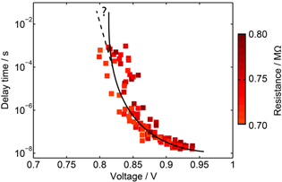
Figure 4. Threshold switching delay time as a function of applied voltage, determined from experiments with constant-voltage pulses. The delay time is defined as the time between the beginning of the application of a voltage and the point in time at which the current through the cell reaches 50 μA. Preceding each constant-voltage pulse with a duration of 1 ms, the mushroom cell was amorphized to have a resistance between 700 and 800 kΩ in order to guarantee comparable initial cell states (the shades of red indicate the individual initial cell resistances according to the colour bar in figure 9). The voltage level of the test pulse was increased stepwise in increments of 10 mV in each series of experiments (starting from 650 mV up to 1 V).
Download figure:
Standard image High-resolution image3.3. Current increase during delay time foretells later switching
Fortunately, our measurement setup provides us with more than just a delay-time for each constant-voltage pulse. We can also look at the transient current signal before the threshold switching event. Without the amplification of the current signal (with decent signal-to-noise-ratio even on rather short time scales) the current before switching would not be distinguishable from zero. The example of a typical data set in figure 5 shows how the transient current before threshold switching looks. We observe a uniform current evolution leading to the threshold event. In order to test whether there is a correlation between the transient behaviour of the current before switching and the incident of switching itself, we determine the pre-switching-slope (preSS) by applying a linear fit to the data for each constant-voltage pulse.

Figure 5. Transient current during a 1 ms long test pulse at a constant voltage of 870 mV. By increasing the voltage to its maximum level within 2 ns, the current rapidly rises to a value of Iinitial ≈ 14 μA (without showing any charging effect, which is in line with the RC-time discussed earlier). During the plateau of the voltage pulse, the current linearly rises over time until the device ends up in threshold switching, which is indicated by the sharp increase in the data. From the rise of the current we determine the pre-switching-slope (short: preSS) by a linear fit.
Download figure:
Standard image High-resolution imageAfter figure 4 showed a clear dependence of the delay time on the applied voltage, figure 6 now shows that there is also a strong dependence of the preSS on the applied voltage. A kink is visible in the curve between 0.80 V and 0.83 V separating two regimes: above that voltage the preSS increases strongly with increasing voltage. In contrast, at voltages below that kink, the preSSs do not only increase much less with increasing voltage, but their absolute values are also extremely small in relation to the resolution of our measurments. The error bars in figure 11 (in the appendix) illustrate that the current increase in this subcritical regime is almost not distinguishable from zero. There are even several (92) data sets where a similarly small negative value for the preSS (−10−2 A s−1 < preSS < −10−6 A s−1) results from the fitting procedure (see supplemental figure 11), again speaking for an almost non-existing current increase in the voltage regime below around 0.8 V.
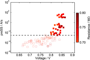
Figure 6. Pre-switching-slope of the current as a function of the voltage applied to the device under test. Filled data points indicate the existence of a threshold switching event within the duration of the voltage pulse. Pulses that do not show threshold switching are represented by open data points. Prior to the test pulse, the device was reset to a cell resistance between 700 and 800 kΩ (the shades of red indicate the individual initial cell resistances according to the colour bar in figure 11). The distribution of filled and open squares orders remarkably over two distinct branches meeting in a pronounced kink in the curve. This points to a correlation between the existence of a significant pre-switching-slope and the observation of threshold switching. (For greater clarity no error bars are plotted in this figure. Instead figure 11 in the appendix provides error bars for these and for further data.)
Download figure:
Standard image High-resolution imageIf one now marks whether during a certain constant-voltage pulse a threshold switching event occurred (filled symbols in figure 6) or not (empty symbols), one finds that the same kink in the preSS versus voltage curve described above also distinguishes the experiments that eventually switched from those that did not. An obvious interpretation of this co-occurrence is that a significantly high preSS foretells the following threshold switching.
From these data, we can derive an important conclusion: the preSS of the current seems to be a measure for the electrical excitation of the amorphous phase change material upon an applied voltage, ultimately leading to threshold switching. This way we can answer the question that arises from our delay time measurements (figure 4), a question that can never be answered unambigously from this kind of experiments for practical reasons. That is, whether at even lower voltages one would only need to wait longer for threshold switching to eventually occur. In the light of our preSS analysis the answer is 'no'. There is no reason to expect that threshold switching should take place at any time when applying subcritical voltages, because from the beginning of the voltage pulse no significant electrical excitation can be observed, which seems to be directly correlated with eventual switching.
3.4. Evidence for electrical field causing current increase prior to switching—not Joule heating
However, one might intervene that the increase of the current through a phase change device could be simply due to Joule heating, and the preSS is therefore no indicator for the degree of electronic excitation. The higher the applied voltage is, the higher is the current already at the beginning of the constant-voltage pulse, and therefore the higher is the deposited power, i.e. heat. And finally, the stronger the increase in temperature is, the higher is the increase of the current due to a more strongly increasing conductivity of the amorphous material.
In order to test this hypothesis, we can check for the dependence of the preSS of the current on the initial electrical power exerted on the device at the beginning of the voltage-pulse. If heating due to the consumption of electrical power is the origin of the current increase, there should be a universal dependence of the preSS on the initial power regardless of the resistance a device originally has. The latter was varied by modifying the intensity of the RESET pulses in a large number of constant-voltage-pulse experiments resulting in figure 7. In the regime of very slow current increase, less than 10−2 A s−1, i.e. at power values lower than around 13 μW, one could argue to see a general trend of increasing preSS with increasing electrical power. Regardless of their initial resistance (indicated as colour of the data points) the results follow such a general trend, implying that there the current increase might be driven by heating. Considering that the preSSs in this regime are ranging around zero (see figure 11 in the appendix), it might be advisable to not interpret too much into these experiments that did not lead to threshold switching (empty symbols). Turning towards those constant-voltage pulses, however, which gave rise to more rapid current increases (more than around 10−2 A s−1) and eventually threshold switching (filled symbols), one has to note that there is no general dependence on the heating power. Instead, it is evident that, in phase change cells with higher initial resistance, the same current increase is produced as in cells with lower initial resistance, despite the fact that much less power is exerted on them. Therefore, one must conclude that Joule heating driven by the electrical power is not what controls the current increase observed before threshold switching. It is noteworthy that a rough estimation of the thermal time constant of the cell structure used in these experiments (depicted in figure 1) should be in the range of 10 ns or less. One should therefore expect the cells to finish thermally responding to the excitation much earlier than after hundreds of microseconds, over which the continuous increase of the current is observed (see e.g. figure 5).

Figure 7. Pre-switching-slope plotted as a function of initial power. The initial power is calculated as the product of the initial current (illustrated in figure 5) and the constant applied voltage. The colour bar indicates the cell resistance before applying the voltage test pulse. Different cell resistances are achieved by varying the height of the reset pulse, which changes the size of the amorphous dome in the mushroom cell. Filled (unfilled) data points represent pulses that show (do not show) a threshold-switching event. At least in the case of constant-voltage-pulse experiments that lead to threshold switching (filled symbols), there is no universal dependence of pre-switching-slope on the consumed electrical power observable, but instead a wide distribution of initial powers leading to the same preSS values. This evidence speaks against Joule heating as the dominant cause of the strong increase in current over time prior to threshold switching. (For greater clarity no error bars are plotted in this figure. Instead figure 12 in the appendix provides error bars for these data.)
Download figure:
Standard image High-resolution imageAnother intervention could be, that partial crystallization of the amorphous volume is responsible for the current increase prior to threshold switching. However, also here, one would have to expect a nonlinear increase in time, as the reduction of badly conducting amorphous material and the according current increase at constant voltage should lead to a higher temperature. This higher temperature in turn would have to result in an increased crystallization speed, implying a super-linear increase of current over time, which is in contrast with what we observe (figure 5).
Thus, we are lead to believe that the measured current increase before threshold switching (preSS) is an indication of electrical excitation towards the swichting and not merely the consequence of Joule heating.
3.5. Meaning for existing theories about electrical excitation of the amorphous phase
The various theories about electric-field-induced threshold switching all provide (different) explanations for the occurrence of an increase of the current prior to the switching. In Ielmini's model, charge carriers are continously excited into shallow traps, leading to a continuous increase in conductivity of the amorphous phase even before the clearly observable threshold switching event (see simulations in [56, 57]). Similarly, in the case of the mechanism proposed by Adler, Raedelli and Pirovano [21, 24, 31], respectively, the interplay between generation and recombination must evolve in time: the filling of trap states reduces the number of potential relaxation centres, which leads to an increasing number of free carriers and accordingly the quasi Fermi level approaching the band edge, therefore increasing the conductivity. And also in the model by Karpov et al [23] in the process of forming highly conductive crystalline nuclei the effective distance between the electrodes is countinuously shortened, thereby steadily reducing the overall resistance of the device.
The existence of a critical electrical field for threshold switching would always have the following consequence. The same constant-voltage pulse applied to an amorphous mark of smaller size, i.e. with a shorter distance between (effective) electrodes, can be sufficient to create an overcritical field leading to threshold switching, while in a bigger amorphous volume the electrical field would remain subcritical and therefore excitation could not build up. This dependence is exactly what we see when plotting the results of constant-voltage-pulse experiments on phase change cells that were reset into states with lower resistance, which indicates amorphous plugs of smaller size. Figure 8 shows that the smaller the amorphous marks are, the lower can the voltages be (e.g. around 0.75 V) that are sufficient to give rise to significant current increases (preSS). And accordingly those lower voltages also lead to threshold switching after finite delay-times (see figure 9).

Figure 8. Pre-switching-slope as a function of applied voltage measured for various initial cell resistances between 300 and 800 kΩ. Filled squares indicate the existence of a threshold-switching event during the applied pulse, whereas unfilled symbols represent experiments in which no switching event occurred. The device resistance shows a pronounced influence on the voltage dependent pre-switching-slope. For smaller initial resistances the curves are shifted towards lower voltages. Because a smaller initial resistance is indicative of a smaller size of the initial amorphous plug, this shift of curves is in line with the increase in current prior to threshold-switching being an effect induced by the electric field. (For greater clarity no error bars are plotted in this figure. Instead figure 11 in the appendix provides error bars for these data.)
Download figure:
Standard image High-resolution image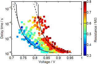
Figure 9. Threshold switching delay time as a function of applied voltage for cells with varying initial amorphous plug size (i.e. initial resistance). In order to investigate the delay time for different amorphous plug sizes, the amplitude of the preceding reset pulse was varied, resulting in cell resistances between 300 and 800 kΩ. In agreement with an electric-field-induced switching-mechanism, a decrease in initial cell resistance, and thus a decrease in amorphous thickness between effective electrodes, results in a lowering of the voltages at which threshold switching takes place after a specific delay time. Although delay times were measured over five orders of magnitude in time, the existence of a minimal threshold field cannot be proven based on such an analysis alone. (The errors of both measured delay times and applied voltages are smaller than the size of the datapoints. Deviations from an ideal curve might be due to variations in the exact shape of an amorphous volume within the tested phase change device.)
Download figure:
Standard image High-resolution imageIn line with the studies of Krebs et al on threshold switching of as-deposited phase change materials in lateral cell structures, our data (in figure 9) also hint towards a finite minimal voltage even at infinitely small amorphous marks (reduction of initial resistance from 0.8 MΩ to 0.4 MΩ shifts critical voltages only from 0.8 V to 0.7 V), pointing towards an electrical interface effect at the contact between electrode material and phase change material [58, 59].
Several contradicting theories on the excitation mechanism behind the phenomenon of threshold switching have been mentioned above. With our current work we present a way to experimentally check their validity. However, all of the existing models contain a number of parameters, which can significantly change their quantitative predictions for the outcome of switching experiments. Of course, the essential material's parameters can remain fixed when using the same composition (here Ge2Sb2Te5). But, for example, sample geometry and electrical capacitances in the setup can strongly change the outcome of an experiment and therefore need to be taken into account. The application of these models on the presented experiments would be a scientific work for itself, especially where predictions cannot be derived analytically but only computed numerically (see e.g. [56, 57]). In principle, though, all of these theories must lead to quantitative predictions about the current increase before threshold switching, which could be critically compared to experimental evidence. While so far most of the time only steady state I–V-characteristics [22, 24, 25, 60–64] and sometimes even delay-times [23, 49, 52–55] are used to match a model to, the evolution of the electrical current preceding threshold switching opens a whole new dimension for testing the validity of theories.
Nevertheless, one hypothesis about how to explain threshold switching after certain delay-times can be addressed already on the basis of our present data. Ielmini et al proposed in some of their papers [55, 56] that threshold switching (especially for longer delay times, i.e. between 100 ns and 10 ms) is triggered by current fluctuations which follow a 1/f behaviour. The underlying assumption here is that there is a rather sharp criterion for the switching to take place; and the longer one waits, the higher the probability that a fluctuation of the current will be large enough to surpass this critical value and trigger the switching accordingly.
In view of the correlation between the preSS of the current prior to switching and the switching event itself, it is reasonable to assume that the preSS is an indicator for the electrical excitation of the amorphous material. If the switching would be triggered by some kind of noise effect, one should see a significant sign of electrical excitation starting only after a period of time without excitation. Our experiments, however, show the contrary, i.e. the electrical excitation is building up already from the beginning of the constant-voltage pulse. Figure 10 illustrates this for four representative experiments with very different delay times ranging over several orders of magnitude.

Figure 10. Representative transient current traces normalized to their individual threshold switching delay time (colour code). Independently of the absolute value of the delay time, all curves show a continuous (and rather linear) increase in current over time starting already at the beginning of the applied voltage pulse (normalized time equal to zero) until the threshold-switching event occurs (normalized time equal to one). For clarity each curve is shifted vertically by several μA.
Download figure:
Standard image High-resolution image4. Conclusion
In conclusion, we investigated the transient evolution of the current through an amorphous phase change material under constant voltage using a custom-made electrical tester in an unprecedented way. The observation of a significant current increase over time prior to the actual threshold-switching event turned out to be a good measure for the electrical excitation taking place. As such it qualified for foretelling the occurrence of threshold switching. Accordingly, under low applied voltages the failure to switch is predicted by a lack of a significant preSS of the current.
Therefore, while the determination of delay times cannot unambiguously clarify the existence of an absolute minimum for the threshold voltage (or field respectively), holding also on timescales beyond the measured range, the investigation of transient currents before switching does. We found experimental evidence for phase change materials intrinsically solving the voltage–time-dilemma of memory applications by the nature of their threshold switching behaviour.
The experimental observation of a continuous increase of current prior to switching also shows that at a sufficient voltage level, the progress of electronic excitation starts right at the beginning of the voltage pulse. This speaks against any mechanism in which statistical fluctuations (like 1/f noise [55]) trigger the threshold switching event after certain delay times.
The physical insights into threshold switching, that were already possible based on the presented electrical characterization techniques, convinced us that the transition region, instead of being just a necessary bridge from unchangingly resistive to excited states, could be a region with a wealth of important information about the physics of the amorphous phase. Extending experimental investigations in this direction has the potential to validate or disprove existing models and inspire new theories on the nature of threshold switching in the future .

Figure A1. Pre-switching-slope as a function of applied voltage for multiple initial cell resistances. Same data as used in figure 8 but including error bars for the preSS values.
Download figure:
Standard image High-resolution image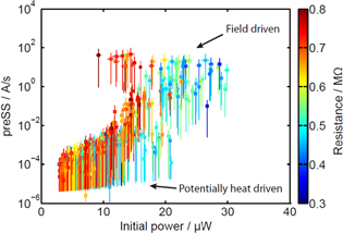
Figure A2. Pre-switching-slope as a function of initial power for different initial cell resistances. Same data as plotted in figure 7, but including error bars for preSS and initial power.
Download figure:
Standard image High-resolution image
Acknowledgments
The authors gratefully acknowledge the financial support by the German Science Foundation (DFG) through the Collaborative Research Centre 'Nanoswitches' (SFB 917). We also thank our partners in the EU-funded 'DIASPORA' project, Daniel Krebs, Abu Sebastian, Manuel Le Gallo and Matthias Kaes at the IBM Zurich Research Laboratory, for stimulating discussions on this topic.
Appendix