


Abstract
We study the system where a superconducting flux qubit is capacitively coupled to an LC resonator. In three devices with different coupling capacitance, the magnitude of the dispersive shift is enhanced by the third level of the qubit and quantitatively agrees with the theory. We show by numerical calculation that the capacitive coupling plays an essential role for the enhancement in the dispersive shift. We investigate the coherence properties in two of these devices, which are in the strong-dispersive regime, and show that the qubit energy relaxation is currently not limited by the coupling. We also observe the discrete ac-Stark effect, a hallmark of the strong-dispersive regime, in accordance with the theory.
Export citation and abstract BibTeX RIS

Content from this work may be used under the terms of the Creative Commons Attribution 3.0 licence. Any further distribution of this work must maintain attribution to the author(s) and the title of the work, journal citation and DOI.
1. Introduction
Dispersive readout is widely used for superconducting qubits, because it potentially enables high-fidelity, fast and non-destructive readout [1]. In this readout scheme, the superconducting qubits are coupled to an electromagnetic resonator (LC resonator) or transmission line, and the type of coupling, i.e. what kind of degree of freedom to use, and its strength should be properly chosen based on various aspects, such as readout fidelity and backaction on the qubits. Note that even for the same type of qubit, we can still choose either capacitive (voltage) or inductive (current) coupling. For example, in charge (or transmon) and phase qubits, both capacitive and inductive couplings have been studied [2–6]. Transmon and phase qubits are (dc-) charge insensitive devices. However, as pointed out by Koch et al [7], this does not mean they are insensitive to the ac voltage field, and the strong coupling regime has indeed been achieved in these devices using capacitive coupling [2, 8].
For the superconducting flux qubits, on the other hand, inductive coupling has typically been used [9, 10]. This may be related to the fact that the states of the flux qubit are often associated with the clockwise and the counterclockwise circulating currents, besides that the flux qubits are also (dc-) charge insensitive devices. Again, however, this does not mean that capacitive coupling is impossible for the flux qubits6. We demonstrated in [13] that we can achieve strong coupling between a conventional flux qubit and an LC resonator coupled via a capacitance. In the paper, we also reported an enhancement of the dispersive shift of the cavity resonance induced by the third level of the flux qubit. This effect was first predicted for the transmon qubit [7] to occur when a specific level configuration, ω01 < ωr < ω12, is realized, where ωij is the qubit transition frequency between the ith and the jth levels and ωr is the cavity resonant frequency. They call this a straddling regime, in which cooperative interplay between 0–1 and 1–2 transitions gives rise to the enhancement of the dispersive shift. In [13], we show that the magnitude of the observed dispersive shift, which was more than four times larger than that estimated from a simple two-level approximation, is quite consistent with the theory which takes into account the higher levels of the flux qubit. We note that the effect of the higher levels of the artificial atom on the dispersive shift has recently been investigated in the fluxonium qubit too [14, 15].
The present paper is an extension of our previous paper [13] and motivated mainly by the following three questions related to the enhancement in the dispersive shift. (i) Why had such a large enhancement never been observed in much more extensively studied devices with inductive coupling? (ii) Does the enhanced dispersive shift affect the coherence of the qubit? (iii) Can the enhanced dispersive shift be applied to anything besides the readout of the qubit? To answer these questions, the rest of the present paper is organized as follows: in section 2, we describe the details of the sample fabrication and the measurements. In the present paper, we study three different devices. In all the devices, a flux qubit is coupled to an LC resonator, but with different magnitude of the coupling capacitance. In section 3, we measure the dispersive shift in the three devices, and compare it with the calculation using the device parameters independently determined by the spectroscopy measurements. Section 4 is related to the first question. We calculate the energy band of the two circuits in the straddling regime, where the flux qubit is coupled to a resonator either via a capacitance or an inductance. Based on that, we discuss the difference in the enhancement of the dispersive shift. Section 5 is to answer the second question, in which we study the coherence property of our devices. The results show that the energy relaxation time is not limited by the coupling at present. Section 6 is related to the third question, where we clearly observe the discrete ac-Stark effect, which is a hallmark of the strong-dispersive regime. We show that the data are well reproduced by the theory. Finally, in section 7, we summarize our results.
2. Sample fabrication and measurements
In this work, we study the system where a superconducting flux qubit is capacitively coupled to a superconducting coplanar waveguide (CPW) resonator (figure 1). The CPW resonator is made of a 50 nm thick Nb film sputtered on a 300 μm thick undoped Si wafer covered by a 300 nm thick thermal oxide. It is patterned by electron-beam (EB) lithography using the ZEP520A-7 resist and CF4 reactive ion etching. The flux qubit is a conventional three-Josephson-junction (3JJ) flux qubit, in which one junction is made smaller than the other two by a factor of α. It is fabricated by EB lithography and double-angle evaporation of Al using PMMA/Ge/MMA trilayer resist. The thicknesses of the bottom and the top Al layers are 20 and 30 nm, respectively. In order to realize a superconducting contact between Nb and Al, the surface of Nb is cleaned by Ar ion milling before the evaporation of Al.

Figure 1. (a) Schematic representation of the device. A 3JJ flux qubit, in which one of the three junctions is smaller than the others by a factor of α, is coupled to a center conductor of λ/2-type CPW resonator via a capacitance Cc. The magnetic flux Φ penetrates the loop of the flux qubit, which is inductively coupled to the control line. The resonator is also coupled to an external transmission line for the readout via a capacitance Cin. (b) Optical image of the device with Cc of 4 fF magnified for the qubit part. (c) Scanning electron micrograph of the three-junction flux qubit. The areas shaded by red represent the Josephson junctions.
Download figure:
Standard image High-resolution imageIn this work, we study the three devices with different coupling capacitances Cc between the qubit and the resonator. We call them devices A, B and C, which have designed Cc of 2, 3 and 4 fF, respectively. All of the devices have a λ/2-type CPW resonator of the same design. They have the fundamental resonant frequency at around 10.25 GHz, and the loaded quality factor Q of ∼650, which is limited by the input capacitance Cin designed to be 15 fF. The qubits have almost the same design in all of the devices, but with small adjustment in α to compensate for the effect of Cc on ω01. The loop has a size of ∼2.0 × 2.4 μm2, and is coupled to the control line by a mutual inductance of ∼0.1 pH.
The devices were mounted in a sample holder made of gold-plated copper, which is thermally anchored to the mixing chamber of a dilution refrigerator and cooled to ∼10 mK. The sample holder is covered by three-layer (one superconducting and two μ-metal) magnetic shields, but we do not use radar-absorbent materials [16] in this work. For the spectroscopy measurements, we used a vector network analyzer. For the measurements of the dispersive shift and qubit coherence, we used a pulsed microwave and for the heterodyne detection of the time-domain data we used a commercial analogue-to-digital converter [13].
3. Dispersive shift in the straddling regime
Before investigating the dispersive shift, we need to experimentally determine the device parameters. As shown in [13], this was done by probing the energy bands of the system by the spectroscopy measurements and fitting the result with the energy bands calculated from the model Hamiltonian (equations (1)–(4) in the next section). Figure 2 shows an example of the spectroscopy measurement for device B. In figure 2(a), we plot the phase of the reflection coefficient Γ as a function of the probe frequency ωp and the flux bias for the qubit f ≡ Φ/Φ0, where Φ is the flux through the qubit loop and Φ0 is the flux quantum. We observe clear vacuum Rabi splitting indicating that the strong coupling regime is achieved. In figure 2(b), on the other hand, we measure Γ at a fixed probe frequency ωp = ωr = 2π × 10.274 GHz, where ωr is the resonant frequency of the resonator when the qubit is in state |0〉, while applying an additional continuous microwave field at ωd to the qubit control port. In the figure, |Γ| is plotted as a function of ωd and f. Figures 2(c) and (d) are the same as figures 2(a) and (b), but the fitting curves are plotted together. As seen in the figures, the data are well fitted by the Hamiltonian (equation (1)), and from this fitting, we extracted the device parameters, which are listed in table 1 for all the devices. In the table, we also listed the parameters of the device used in [13]. The obtained Cc are quite consistent with the designs.
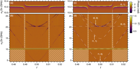
Figure 2. Spectroscopy of the coupled system (device B). (a) Phase of the reflection coefficient Γ as a function of the flux bias and the probe frequency. (b) |Γ| as a function of the flux bias and the qubit excitation frequency. |Γ| is normalized by the value measured at ωr without the qubit drive. The same data as in (a) are shown in the green box for comparison. There are no data in the regions filled with the meshes. Panels (c) and (d) are the same as (a) and (b), respectively, but the result of the fitting is overlaid by the white dashed curves. Labels on the energy levels denote the corresponding excitation from the ground state, namely, |q,r〉 indicates that the qubit and the resonator are in the qth and the rth states, respectively.
Download figure:
Standard image High-resolution imageTable 1. Parameters of the measured devices.
| Designed | Fitting parameters | |||||
|---|---|---|---|---|---|---|
| Device | Cc (fF) | Cc (fF) | EJ/h (GHz) | Ec/h (GHz) | α | Er/h (GHz) |
| A | 2 | 1.86 | 139 | 3.55 | 0.685 | 10.250 |
| B | 3 | 3.14 | 146 | 3.38 | 0.640 | 10.252 |
| C | 4 | 4.19 | 148 | 3.29 | 0.613 | 10.298 |
| [13] | 4 | 4.08 | 148 | 3.27 | 0.611 | 10.679 |
Next, we investigate the dispersive shift. Using a pulsed readout, we measure Γ as a function of ωp. By applying a π-pulse to the qubit before the readout, we can measure Γ corresponding to the qubit state |1〉. The pulse sequence is shown in the inset of figure 3. We use 100 ns long time trace data of the reflected readout pulse, which starts after a delay td from the termination of the π-pulse, to extract the amplitude and the phase. The delay td is adjusted to give a maximum contrast between the qubit states |0〉 and |1〉. Figure 3 shows the amplitude of the normalized reflection coefficient Γ' as a function of ωp. Γ' is defined as Γ' ≡ (Γ − Γon)/|Γoff − Γon|, where Γon and Γoff are the reflection coefficients obtained by the on and the off resonance of the resonator, respectively [13]. For each device, we measure |Γ'| with and without the π-pulse, where the qubit is biased at f = 0.5. The shifts of the dip frequency correspond to the dispersive shifts. The observed dispersive shifts 2χ and ωr are summarized in table 2, together with ω01 determined by the spectroscopy measurements. In the table, we also listed the theoretical parameters obtained from the energy band calculation using the fitting parameters listed in table 1. The measured dispersive shifts are close to the theoretical predictions which are obtained by calculating the difference between the cavity resonant frequencies when the qubit is in state |0〉 and state |1〉. Their magnitudes are much larger than the values estimated under the two-level approximation for the qubit, namely, |g201/Δ01|, where Δ01 = ω01 − ωr. Here, g01 represents the matrix element  , where |0〉 and |1〉 are the ground and the first-excited states of the uncoupled qubit Hamiltonian (equation (2)), respectively, and
  is the coupling Hamiltonian
  (equation (4)) restricted onto the qubit subspace. This enhancement is due to the effect of the straddling regime [7]. As seen in table 2, the condition for the straddling regime ω01 < ωr < ω12 is satisfied in all the devices.
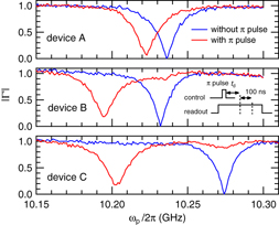
Figure 3. Dispersive shifts in all of the devices. The normalized reflection coefficient |Γ'| is plotted as a function of the frequency of the probe microwave field ωp. Blue (red) traces represent |Γ'| when the π pulse is turned off (on). The inset shows the sequence of the pulses applied to measure |Γ'|.
Download figure:
Standard image High-resolution imageTable 2. Magnitude of the dispersive shift. All of the parameters are for the qubit bias f = 0.5.
| Device | Measured | Theory | |||||
|---|---|---|---|---|---|---|---|
| ω01/2π (GHz) | ωr/2π (GHz) | 2χ/2π (MHz) | 2χ/2π (MHz) | ω01/2π (GHz) | ω12/2π (GHz) | g01/2π (MHz) | |
| A | 3.730 | 10.236 | −13 | −10.7 | 3.727 | 17.61 | 76.0 |
| B | 4.728 | 10.232 | −37 | −35.9 | 4.725 | 15.58 | 143 |
| C | 5.350 | 10.274 | −71 | −71.8 | 5.361 | 14.46 | 201 |
| [13] | 5.504 | 10.656 | −80 | −71.5 | 5.513 | 14.54 | 197 |
4. Comparison between the capacitive and the inductive couplings
As shown in the previous section and in [13], we observed a large enhancement of the dispersive shift of the cavity resonance due to the effect of the straddling regime [7]. It was observed in the system shown in figure 4(a), where a flux qubit is coupled to an LC resonator. However, a natural question is why this had not been reported before in much more extensively studied flux-qubit circuits with inductive coupling (figure 4(b)). Since the flux qubits typically have large anharmonicity, satisfying the condition for the straddling regime, namely, ω01 < ωr < ω12, is quite easy. In fact, we even unintentionally satisfied this condition in our previous study using inductive coupling, but we did not observe such a large enhancement [17]. The purpose here is to answer this question.
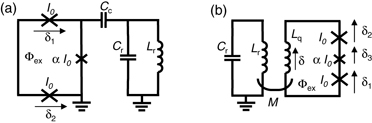
Figure 4. The circuit diagram of (a) a flux qubit capacitively coupled to an LC resonator and (b) a flux qubit inductively coupled to an LC resonator.
Download figure:
Standard image High-resolution imageThe Hamiltonian of the system where a flux qubit is capacitively coupled to an LC resonator as shown in figure 4(a) is given by

which consists of the qubit part, the resonator part and the coupling part. Each term of the Hamiltonian is given as below [13]:


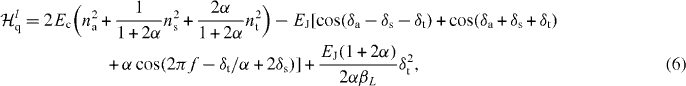
where EJ = I0Φ0/2π, f = Φex/Φ0, Φ0 = h/2e, Ec = e2/2CJ,  , V =(1 + α)(1 + γ) + βc, W = α(1 + γ) + βc, X = (1 + 2α)(1 + γ) + 2βc, Y =1 + 2α + 2βc, βc = Cc/CJ and γ = Cc/Cr. Here, I0 and CJ are the critical current and the capacitance of the larger Josephson junction of the qubit, respectively. δi and ni (i = 1, 2) are the phase differences across the larger junction, and its conjugate variable representing the charge number, respectively. a (a†) is the annihilation (creation) operator of the photons in the resonator. Finally, Lr and Cr are the equivalent inductance and the capacitance of the resonator, respectively.
Next, we consider the Hamiltonian of the system where a flux qubit is inductively coupled to an LC resonator as shown in figure 4(b). The derivation is given in appendices A and B. The Hamiltonian is given by

and each term is given as follows:
where βL = αLq/[(2α + 1)LJ], LJ = Φ0/(2πI0) and Lq is the loop inductance of the flux qubit. Here, we used the following variable transformations for δ (phase across the loop inductance of the qubit) and δi (i = 1,2,3 phases across the junction):


and nt, ns and na are the corresponding conjugate variables.  is given by

 is given by

where EM = Φ20/(2M) and ELr = Φ20/(2Lr).
Based on these, we compare the energy band structure of the two systems. Figures 5(a)–(c) show the excitation energy from the ground state, the coupling strength |gij| and the dispersive shift χij, respectively, for the capacitive coupling case. Here,  , where |i〉 represents the ith eigenstate of the uncoupled qubit Hamiltonian (equation (2)), and χij = |gij|2/(ωij − ωr), where ωij = ωj − ωi. The parameters are taken from device C, namely, EJ = 148, Ec = 3.29 GHz, α = 0.613, Cc = 4.19 fF and ωr/2π = 10.298 GHz. Figures 5(d)–(f) show the corresponding calculations for the inductive coupling case. The qubit parameters, EJ, Ec and α, are kept the same as those for the capacitive coupling case. The mutual inductance M = 8.90 pH and the resonator frequency ωr = 13.80 GHz are chosen in such a way that |g01| and ω01 − ωr, and hence, χ01 become almost equal for both of the coupling cases. By comparing figures 5(c) and (f), we see that the total dispersive shift χtotal for the inductive coupling case is much smaller than that for the capacitive coupling case. Here, χ total is obtained by calculating
  with M = 4, and confirmed to be very close to the result obtained by the energy band calculation [13]. χtotal at f = 0.5 is 8.6 MHz for the inductive coupling, while that for the capacitive coupling is 35.9 MHz. Note that the condition for the straddling regime, ω01 < ωr < ω12, is satisfied in both cases. Indeed, the magnitude of χtotal is larger than that of χ01, meaning that it is enhanced by the effect of the straddling regime. However, the degree of the enhancement is very different for the two cases.
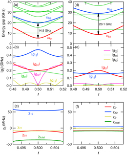
Figure 5. Comparison between the capacitive (a)–(c) and the inductive (d)–(f) couplings. Panels (a) and (d) show the energy gap from the ground state, (b) and (e) show the coupling strength  , and (c) and (f) show the dispersive shift χij. For all the figures, EJ = 148, Ec = 3.29 GHz and α = 0.613 are used. For (a)–(c), Cc = 4.19 fF and ωr/2π = 10.30 GHz are used. For (d)–(f), Lq = 50.0 pH, M = 8.9 pH and ωr/2π = 13.8 GHz are used.
Download figure:
Standard image High-resolution imageThere are two main reasons that make this difference. Firstly, by comparing figures 5(a) and (c), we see that ω12 is much smaller for the capacitive coupling case. Since the qubit parameters are the same, this reduction is due to Cc. This leads to smaller |Δ12| = |ωr − ω12|, and hence larger χ12. Secondly, by comparing figures 5(b) and (e), we see that |g12|/|g01| is larger for the capacitive coupling case. The |g12|/|g01| at f = 0.50 is 2.4 for the capacitive coupling, while that for the inductive coupling is 0.77. This also leads to larger χ12 in the capacitive coupling case. Thus, we conclude that the capacitive coupling plays an essential role in the observed large enhancement of the dispersive shift.
We can also choose the parameters in such a way that the qubit transition energies (ω01 or both ω01 and ω12) are similar in the capacitive and the inductive coupling cases. The results are shown in appendix C. The conclusion that |g12|/|g01| and χtotal are larger for the capacitive coupling case is the same.
5. Coherence times
We investigate the coherence properties of the flux qubit capacitively coupled to the resonator. Figure 6 shows an example of the measurements of (a) the energy relaxation and (b) the echo dephasing in device C, where the qubit is biased at f = 0.5004. The heterodyne voltage V0, which is offset in such a way that it becomes zero when the qubit is in the ground state, is plotted as a function of the delay time. The pulse sequence for each measurement is shown in the inset of the figure. The data for the energy relaxation measurement are well fitted by an exponential decay of  and give the qubit energy relaxation time T1. The oscillation observed in the echo measurement is due to the fact that the rotation axis of the second π/2 pulse is rotated at 100 MHz. It is not so clear whether the decay envelope is exponential or Gaussian. In the figure, we fitted the data by an oscillating Gaussian, namely,
 ![$\exp \,(-t/2T_1)\exp \,[-(t/\tau _{{\rm echo}})^2]\sin \,(\omega t + \phi )$](https://content.cld.iop.org/journals/1367-2630/16/1/015017/revision1/nj482761ieqn11.gif) and extracted the echo decay time τ echo.
and extracted the echo decay time τ echo.
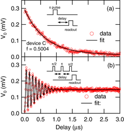
Figure 6. Example of the qubit coherence measurements: (a) energy relaxation and (b) echo decay in device C. The flux qubit is biased at f = 0.5004. The heterodyne voltage V0 is plotted as a function of the delay time in the pulse sequence shown in the inset. The open circles are experimental data and the black curves are the fitting curves.
Download figure:
Standard image High-resolution imageWe measured the flux bias dependence of T1 and τecho in devices B and C, and plot them in figures 7(a) and (c), respectively. T1 is independent of f in the measured range, and the magnitude is almost the same for both devices in spite of their difference in coupling capacitance. In the figure, we also plot the theoretical predictions based on the Purcell effect, κ(g01/Δ01)2 [7]. The observed T1 are more than one order of magnitude below the Purcell limit, and probably limited by something which commonly exists in both devices, such as the two-level systems at the surface of the substrate [18, 19].
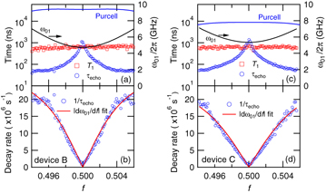
Figure 7. Flux bias dependence of the coherence times. In (a) and (c), the energy relaxation time T1 and the echo decay time τecho are plotted as a function of the flux bias f for devices B and C, respectively. In the figures, qubit |0〉–|1〉 transition frequency ω01/2π obtained by the spectroscopy measurement is plotted by the black curves. Theoretical prediction for T1 limited by the single-mode Purcell effect is plotted by the blue curves. In (b) and (d), 1/τecho is plotted as a function of f for devices B and C, respectively. The red curves represent the |∂ω01/∂f| fitting.
Download figure:
Standard image High-resolution imageThe observed τecho also looks very similar in the two devices. It becomes maximum at f = 0.5 and rapidly decreases as we move away from this bias point. To account for this flux dependence of τecho, we assumed the dephasing due to the 1/ν flux noise (ν is the frequency), which was carefully studied for the flux-qubit circuit with the dc-SQUID (superconducting quantum interference device) readout [20]. We fitted 1/τecho by the derivative of ω01 with respect to f, namely,

as shown in figures 7(b) and (d). In both devices, the fitting looks good, and the fitting parameter A is determined to be 6.6 × 10⁻⁶ and 6.4 × 10⁻⁶ for devices B and C, respectively. These values are of the same order as those reported previously [20–22], supporting the scenario of dephasing due to the 1/ν flux noise.
As shown in the figure, τecho saturates at ∼1 μs at f = 0.5. Note that τecho is the pure dephasing time and should not be limited by 2T1. One possible source of the limit is the dephasing induced by the fluctuations of the photon number in the resonator [1, 23–25]. In the present devices, the cavity decay rate (κ/2π = fr/Q) is about 15 MHz, and the qubit decay rate (γ/2π = T−11/2π) is about 230 kHz. Thus, devices B and C are in the strong-dispersive regime [26], which means that 2χ > κ,γ. As shown in [25], the dephasing rate due to the photon number fluctuations in the strong-dispersive regime is given by

where 〈n〉 is the mean photon number in the resonator and N corresponds to the N-photon resonator state. Since the present data were measured using the fundamental qubit transition frequency (N = 0),7 τ−1 photon is simply given by κ〈n〉, which does not depend either on χ or f. To account for the τecho of 1 μs with given κ, 〈n〉 of 0.01 (or the effective temperature Teff of the resonator of 0.1 K with the assumption that ![$\langle n \rangle = [\exp \,(\hbar \omega _{{\rm r}}/k_{{\rm B}}T_{{\rm eff}})-1]^{-1}$](https://content.cld.iop.org/journals/1367-2630/16/1/015017/revision1/nj482761ieqn12.gif) ) is needed, although at present we do not precisely know the actual value of 〈n〉.
) is needed, although at present we do not precisely know the actual value of 〈n〉.
6. Observation of the discrete ac-Stark effect
As shown in the previous section, devices B and C are in the strong-dispersive regime [26]. The hallmark of this regime is the appearance of separate spectral lines of the qubit transition frequency, each of which corresponds to a particular photon number state of the resonator. This effect can be applied to characterize the photon statistics in the resonator [26]. Here, we investigate this effect using device C.
We measured the reflection coefficient Γ of the probe field (frequency ωp/2π and power Pp) applied via the readout port, by varying the frequency ωd/2π and the power Pd of the qubit drive field applied via the control port. Figure 8 shows |Γ| as a function of Pd and ωd, where ωp is fixed at ωr/2π = 10.274 GHz. Pp is −140 dBm for figure 8(a) and −130 dBm for figure 8(b), which correspond to the mean photon number in the resonators of 0.06 and 0.6, respectively. In the strong-dispersive regime, the qubit transition frequency depends on the resonator photon number N as ω01 − 2Nχ (N = 0,1,2,...), and we expect to observe separate spectral lines at these frequencies. In figure 8(a), we observe a spectral line at ω d/2π = 5.350 GHz at low Pd. This frequency is equal to ω01/2π (see table 2) and corresponds to the zero-photon state. As we increase Pd, another spectral line at 5.279 GHz appears. This frequency is equal to (ω01 − 2χ)/2π and corresponds to the one-photon state. The result of the same measurement with 10 dB higher Pp is shown in figure 8(b). The larger Pp produces the population of higher photon-number states. Indeed, we observe more spectral lines up to the two-photon state.
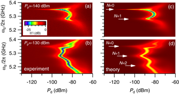
Figure 8. Observation of the discrete ac-Stark effect. The magnitude of the reflection coefficient Γ is plotted as a function of the power Pd and the frequency ωd of the qubit drive. The frequency of the probe microwave is fixed at ωr/2π = 10.274 GHz, and its power is fixed at (a) −140 dBm and (b) − 130 dBm. Panels (c) and (d) are the numerical simulations corresponding to (a) and (b), respectively. The white arrows indicate the qubit frequency when the resonator contains N photons (N = 0,1,2).
Download figure:
Standard image High-resolution imageNote that the observed spectral lines are dips, not peaks. Without the qubit drive, a shallow (< 1 dB) dip is observed at ωr (data not shown) due to the finite internal quality factor (∼ 3 × 10⁴) of the resonator. Thus, a small increase in |Γ| is naively expected when the qubit excitation induces the dispersive shift of the cavity resonance, although the expected magnitude of the signal (< 1 dB) is anyway much smaller than that observed here. The origin of these deep dips is inelastic scattering [27], which is intuitively understood as follows.
Figure 9 shows the level structure of the qubit–resonator system in the dispersive regime in a frame rotating at the qubit drive frequency ωd. Here, we consider only the lowest two levels for the qubit, |0〉q and |1〉q: the higher levels do not play an essential role here, except that they enhance the magnitude of the dispersive level shift [13]. Figure 9(a) represents the energy diagram when the qubit drive is turned off. The label for each level |m,n〉 represents the state where the qubit is in the mth state and the resonator is in the nth state. Note that |m,n〉 is not a simple product of Fock states of the uncoupled qubit and the resonator due to the coupling gij. However, in the dispersive regime, gij mixes the two states |i〉q|n + 1〉r and |j〉q|n〉r only slightly and produces a dispersive level shift. As a result, the level spacings of the left ladder (|0〉q) and the right ladder (|1〉q) in figure 9(a) become different. Since there is no qubit drive, the microwave transition is of cavity origin and occurs vertically within each ladder. The probe field, which is adjusted at the transition frequency of the left ladder, is then scattered elastically.
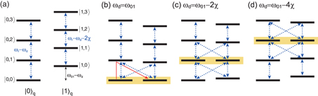
Figure 9. Level structure of the driven qubit–resonator system in the frame rotating at ωd. The blue arrows indicate the allowed microwave transitions. Since the cavity decay rate is much larger than the qubit decay rate, only the transitions induced by the probe field are indicated. (a) Without driving (E = 0). The microwave transitions occur only vertically. (b)–(d) With driving (E ≠ 0). The drive frequency is tuned at ωd = ω01 in (b), ωd = ω01 − 2χ in (c) and ωd = ω01 − 4χ in (d). Oblique transition paths are generated by the mixing induced by the resonant driving of the qubit. Yellow boxes indicate the degenerate two levels, which are mixed strongly by the drive. The red arrow in (b) represents the Raman transition induced by the probe microwave field tuned at ωr.
Download figure:
Standard image High-resolution imageIn contrast, when the qubit drive is turned on, state mixing between the two ladders can happen. For example, when ωd = ω01, |0,0〉 and |1,0〉 become degenerate (figure 9(b), yellow box), and these two states mix strongly. This gives rise to a new radiative decay path from the first excited state of the left ladder (originally |0,1〉) to the ground state of the right ladder (originally |1,0〉). Accordingly, the probe field can induce the Raman transition (red arrow in figure 9(b)). This inelastic scattering results in the reduction of the reflection coefficient. We can expect a similar reduction in |Γ| when ωd is adjusted to be ω01 − 2Nχ as shown in figures 9(c) and (d) for N = 1 and 2, respectively. As we increase the probe power and accordingly the mean photon number in the resonator, we are able to see the effect for larger N, which is what we observed in figure 8(b).
To understand the experimental results more quantitatively, we analyzed the microwave response of this system using a full-quantum theoretical model in which the qubit, the resonator and the propagating microwave modes are treated quantum mechanically, and calculated the reflection coefficient |Γ| (figures 8(c) and (d)) assuming the same parameter values in the experiment. The details of the calculation are summarized in appendix D. We observe fairly good agreement between the experiment and the theory.
7. Conclusion
In conclusion, we studied systematically the system where a superconducting flux qubit is capacitively coupled to an LC resonator. In all three devices with different coupling capacitances, the dispersive shifts are enhanced by the effect of the straddling regime, which is quantitatively reproduced by the theory. We showed by numerical calculation that the capacitive coupling has two effects on the dispersive shift, namely, to reduce the qubit anharmonicity and to produce the large matrix element g12, both of which lead to the large enhancement in χ. We investigated the coherence properties in these devices. Even in the device with the largest Cc (device C) the observed T1 is one order below the Purcell limit. We also showed that the flux dependence of the echo dephasing is consistent with the low-frequency flux noise. We also demonstrated the discrete ac-Stark effect using the device in the strong-dispersive regime. The results can be explained by the inelastic scattering of the microwave incident on the resonator, and well reproduced by the numerical calculations.
Acknowledgments
The authors are grateful to F Yoshihara for a useful discussion. Sputtered Nb films were fabricated in the clean room for analogue–digital superconductivity (CRAVITY) in the National Institute of Advanced Industrial Science and Technology (AIST). This work was partly supported by the Funding Program for World-Leading Innovative R&D on Science and Technology (FIRST), Project for Developing Innovation Systems of MEXT, MEXT KAKENHI (grant numbers 21102002 and 25400417), SCOPE (111507004) and National Institute of Information and Communications Technology (NICT).
Appendix A.: Single flux qubit with non-negligible loop inductance
Here, we derive the Hamiltonian and the central equation for a single flux qubit, where we explicitly take into account the loop inductance. The derivation is based on [28], but with a difference that the periodicity of the potential terms in the Hamiltonian is taken into account. Probably because of this difference, the calculated energy bands do not have the doublet structure reported in [28].
First, we consider a single 3JJ flux qubit with a loop inductance as shown in figure A.1(a). From the flux quantization,

We introduce a dimensionless parameter representing the ratio between the loop inductance and the Josephson inductance


where

Following [28], we perform the following variable transformations:


or equivalently


The potential energy of the JJs is expressed by

where EJ = Φ0I0/(2π). The energy of the loop inductance is


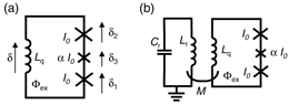
Figure A.1. The circuit diagram of (a) a single 3JJ flux qubit with non-negligible loop inductance and (b) a flux qubit inductively coupled to an LC resonator.
Download figure:
Standard image High-resolution imageThe kinetic energy of the JJs is

where CJ is the capacitance of the larger JJ. Using equations (A.8) and (A.10)

Note that there are no cross terms such as  thanks to the variable transformation. The Lagrangian of the system is

and the canonical momentum is

where i = a, s and t. Finally, the Hamiltonian is given by


where Ec is defined for a single charge, namely Ec = e2/(2CJ). This Hamiltonian can be regarded as a 3JJ flux qubit without the loop inductance interacting with a harmonic oscillator. The harmonic oscillator part (third and fifth terms in equation(A.20)) can be transformed as


As in [28], we choose for our basis functions the product states

where the first two states are plane waves


and the third state is a harmonic oscillator wave function in δt

where Hm[δ] is the mth Hermite polynomial. The wavefunction of the Hamiltonian is given by

where the first sum of k and l is taken for the reciprocal lattice of UJ(k,l) [29]. The qubit potential energy has the following translational symmetry with respect to δa and δs


Thus, its symmetry forms a two-dimensional face-centered lattice as shown in figure A.2(a). It is not a simple square lattice, which is due to the variable transformation. The corresponding reciprocal lattice is also a face-centered lattice shown in figure A.2(b). Thus, the sum for (k,l) in equation (A.28) must be taken for this lattice, and how many points we should take depends on what accuracy we need. Using  , the Schrödinger equation
  is written as
where  means
means  . By multiplying 〈ϕk'l'm'| on both sides, we obtain the following central equation:
To solve the above equation, we use the following formula [30]:

where |m〉 is the mth eigenfunction of the harmonic oscillator and c is a constant which can be a complex number. For example, to calculate 〈ϕtm'|eiδt|ϕtm〉, we use the above formula with


By numerically solving the central equation (A.33) for (k',l') in the subset of the reciprocal lattice and m' from 0 to a certain number, we obtain the energy band diagram for a flux qubit with non-negligible loop inductance.
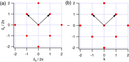
Figure A.2. (a) Real space lattice of UJ and (b) the reciprocal lattice. The arrows represent the unit vectors.
Download figure:
Standard image High-resolution imageAppendix B.: Flux qubit inductively coupled to an LC resonator
Next, we consider a flux qubit inductively coupled to an LC resonator as shown in figure 1(b). The Hamiltonian consists of three parts, namely,

 is already shown in equation (A.20).
  is simply given by

where 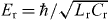 , and a (a†) is the annihilation (creation) operator of the photons in the resonator.
  is given by

Using equations (A.3), (A.5) and

we obtain


where we defined


The matrix elements 〈ϕklm|δt|ϕk'l'm'〉 are given by

And the last term is given by
In the calculation of figure 5(d), 121 reciprocal lattice points are used for k and l, while m is taken from 0 to 2. The number of bases used for the resonator state is 5.
Appendix C.: Numerical calculation with different parameters
In this appendix, we show the results of the numerical calculation for the inductively coupled system of the qubit and the resonator, but with different parameters from those used in figure 5. Figures C.1(a)–(c) show the flux bias dependence of the excitation energy from the ground state, the coupling strength |gij| and the dispersive shift χij, respectively. Here, we adjusted the qubit parameter α in such a way that ω01 is almost equal to that for the capacitive coupling case (figures 5(a)). Also, the mutual inductance M is adjusted so that |g01| becomes almost equal to that for the capacitive coupling case (figure 5(b)). Similar to the results shown in figures 5(e) and (f), |g12|/|g01| and χtotal are much smaller than those for the capacitive coupling case. We can also adjust the qubit parameters (Ec and α) such that both ω01 and ω12 are similar to those for the capacitive coupling case. As shown in figures C.1(d)–(f), the overall behavior is the same, which indicates that the smaller |g12|/|g01| is not due to the larger anharmonicity.
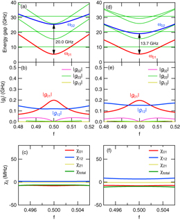
Figure C.1. Numerical calculations for the inductively coupled system of the qubit and the resonator. Panels (a) and (d) show the energy gap from the ground state, (b) and (e) show the coupling strength 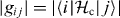 and (c) and (f) show the dispersive shift χij. For (a)–(c), EJ = 148, Ec = 3.29 GHz, α = 0.671, Lq = 50.0, M = 10.2 pH and ωr/2π = 10.3 GHz are used. For (d)–(f), EJ = 148, Ec = 1.80 GHz, α = 0.602, Lq = 50.0, M = 12.0 pH and ωr/2π = 10.3 GHz are used.
Download figure:
Standard image High-resolution imageAppendix D.: Theory of microwave response of the qubit–resonator system
In this appendix, we analyze the microwave response of the present qubit–resonator system. Figure D.1 is a schematic of the theoretical model, which consists of a superconducting qubit, a resonator and waveguides. The lowest two levels of the qubit (|0〉 and |1〉) are relevant here in essence. However, to account for the dispersive level shift due to the second excited state |2〉 [13], we incorporate this level in our model. We refer to the readout line coupled to the resonator as waveguide 1, and the qubit control line as waveguide 2. We apply a monochromatic field E(t) = Ee−iωdt to drive the qubit through waveguide 2. By defining v as the microwave velocity in the waveguides, the Hamiltonian of the system is


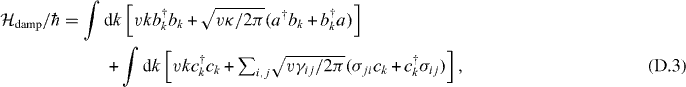
where σij = |i〉〈j| is the transition operator of the qubit, a is the annihilation operator of the resonator and bk (ck) is the annihilation operator of the photon propagating in waveguide 1 (2) with wavenumber k.  is the bare eigenenergy of the jth qubit level with
  (the eigenenergy of
  , equation (2)),
  is the bare resonator frequency (
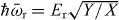 (see equation (3))), gij is the qubit–resonator coupling, κ is the resonator decay rate and γij is the qubit decay rate for the |j〉 → |i〉 transition. From the parity selection rule and the rotating-wave approximation, gij and γij are non-zero only for (i,j) = (0,1) and (1, 2).

Figure D.1. Theoretical model. A qubit is coupled dispersively to a resonator, which is further coupled to the readout line (waveguide 1). The qubit is driven by a microwave field propagating along the qubit control line (waveguide 2).
Download figure:
Standard image High-resolution image
By switching to a frame rotating at the drive frequency ωd, the Hamiltonian becomes static.  is then given by

 remains unchanged except that the photon frequency is measured from ωd. We define the dressed states of the qubit–resonator system as the eigenstates of
  . We denote them by
  and their energies by
  (j = 1,2,...) from the lowest.
  corresponds to the states shown in figures 9(b)–(d), or the states in figure 9(a) if E = 0. In the dressed-state basis, the Hamiltonian of the overall system is rewritten as


where  ,
,  (
( ) is the radiative decay rate into waveguide 1 (2) for the
  transition. They are, respectively, given by


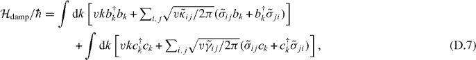
We work in the dressed-state basis to analyze the microwave response of the system to a probe field applied from waveguide 1. From equation (D.5), the Heisenberg equation for  is
is
where bin (cin) is the input field operator for waveguide 1 (2). By denoting  (μ = κ,γ), the coefficients ηijmn and ξμijmn are given by


We apply a probe field with amplitude F and frequency ωp from waveguide 1, while we apply no probe field from waveguide 2. Therefore, 〈bin(t)〉 = Fe−i(ωp−ωd)t and 〈c in(t)〉 = 0. Note that the probe frequency ωp is measured from the drive frequency ωd in the rotating frame. The stationary solution of the equation (D.10) is then written as

Substituting equation (D.13) into equation (D.10) and solving the linear simultaneous equations together with the condition that  , i.e.
  , we numerically determine Amij. Reliable numerical results are obtained by setting −2 ⩽ m ⩽ 2 and 1 ⩽ i,j ⩽ 8. The output field amplitude 〈bout(t)〉 for waveguide 1 is related to the input one by 〈bout(t)〉 = 〈bin(t)〉 − i〈Sκ(t)〉. The reflected field contains high-order harmonics due to the nonlinear effect. However, in the reflectivity measurement, only the field at the fundamental frequency (m = −1) is relevant. The reflection coefficient is defined by Γ = 〈bout(t)〉m=−1/〈bin(t)〉m=−1. Therefore,

In the numerical simulation, we have chosen the bare parameters of the qubit–cavity system ( ,
,  , g01 and g12) to reproduce the following experimentally measured parameters, ω01/2π = 5.35 GHz, ωr/2π = 10.27 GHz and 2χ/2π = 71 MHz. We have set κ/2π = 15 MHz as stated in the main text. We employed the qubit radiative decay rate into waveguide 2 as γ10, which is estimated to be γ10/2π = 88 Hz from the Rabi oscillation measurement. We determined F based on the experimental parameter Pp. γ21 has almost no effect on the numerical results.
Footnotes
- 6
- 7
In the spectroscopy measurement, we observed separate qubit spectral lines corresponding to N = 0,1 and 2 as shown in the next section.