


Abstract
Si films sputter deposited on thermally oxidized Si are enriched with Ga by ion implantation through a SiO2 capping layer. The morphology and the electrical transport properties of these films are investigated after rapid thermal annealing. Amorphous, Ga-rich nanoinclusions are embedded in a nanocrystalline Si matrix. The metallic nanoinclusions become superconducting below 7 K. They form a random network of junctions to heavily doped Si crystallites. Small modifications of the junction properties, e.g. by annealing or current pulses, can dramatically change the electronic transport in the film. Ga-rich Si films show a wealth of low-temperature transport phenomena, which have been known until now only from granular metals or high-temperature superconductors: superconductor–insulator transition, quasi-reentrant superconductivity and current-controlled sheet resistance. The possibility to prepare and modify Ga-rich Si films with microelectronics-compatible technology makes them interesting for both fundamental research on transport phenomena in nanostructured, disordered superconductors as well as for the integration of superconducting circuits into Si devices.
Export citation and abstract BibTeX RIS

Content from this work may be used under the terms of the Creative Commons Attribution 3.0 licence. Any further distribution of this work must maintain attribution to the author(s) and the title of the work, journal citation and DOI.
GENERAL SCIENTIFIC SUMMARY Introduction and background. Extreme doping of standard semiconductor materials with suitable impurity atoms up to concentrations of several atomic percent can equip them with new functionalities like ferromagnetism or superconductivity. Semiconductors modified in this way could serve as base materials for future information technologies, such as spintronics or quantum computing.
Main results. We found that Ga-rich Si films prepared by ion implantation and rapid thermal annealing are superconductors or insulators in dependence of the processing conditions. These films consist of Ga-rich nanoinclusions embedded in a heavily doped Si:Ga matrix. The nanoinclusions become superconducting below 7 K. They form a random network of junctions to heavily doped Si crystallites. Small modifications of the junction properties, e.g. by annealing or current pulses, can dramatically change the electronic transport in the film. The superconducting inclusions can couple coherently if the sheet resistance of the matrix drops below a critical value, otherwise the films behave insulating.
Wider implications. Ga-rich Si films show a wealth of low-temperature transport phenomena which have been known until now only from quite different systems such as granular metals or high-temperature ceramic superconductors: superconductor-insulator transition, quasi-reentrant behavior and current-controlled sheet resistance. The possibility to prepare and modify Ga-rich Si films with microelectronics-compatible technology makes them interesting for both fundamental research on transport phenomena in nanostructured, disordered superconductors, as well as for the integration of superconducting circuits into Si devices.
 Figure. Si films with Ga-rich inclusions (bright regions in the film cross-section) become superconducting (red curve) or insulating (blue curve) in dependence of the annealing conditions.
1. Introduction
Extreme doping of standard semiconductor materials with suitable impurity atoms up to concentrations of several atomic per cent can equip them with new functionalities. Dilute magnetic [1] or superconducting semiconductors [2–4] could serve as base materials for future information technologies, such as spintronics [5, 6] or quantum computing [7]. Much technological effort has been devoted to overcome doping limits set by the equilibrium solid solubility of the impurities and to fabricate homogeneous layers of such materials [8–11]. Nevertheless, semiconductor layers with extreme dopant concentration tend to decompose during further processing by impurity precipitation in the film or segregation at interfaces. Alternatively, one can try to use impurity precipitates directly to functionalize the semiconductor properties [12–14]. For this purpose, precipitation and its influence on the properties of such heterogeneous semiconductor films have to be understood and controlled.
It is known that heterogeneous (e.g. granular) or disordered (e.g. amorphous) metal or composite films can dramatically change their transport properties under tiny variations of film structure, composition or external fields [15–17]. Metal–insulator transitions (MIT) or even superconductor–insulator transitions (SIT) have been observed. In contrast to homogeneous superconductors with a sharp transition to a zero-resistance state that persists at all temperatures below the critical one, heterogeneous films can demonstrate a complex, non-monotonic resistance versus temperature curve in the temperature range where Cooper-pair condensation takes place. Phenomena such as incomplete transitions, reentrant (the loss of superconductivity at a temperature lower than the critical one) or quasi-reentrant (presence of a resistance minimum) superconductivity have been observed [18–21]. It is an open question whether such effects are also present in semiconductor films with superconducting precipitates and how they are related to structural details.
Recently, we reported about robust superconductivity [12, 22, 23] below a critical temperature of 7 K and a SIT controlled by annealing conditions [24] in Si layers implanted with high fluences of Ga ions. No obvious differences in the morphology of the Ga-rich Si (Si:Ga) layers have been detected which could explain the phase transition [24]. Instead, a critical sheet resistance (R ∼ 13 kΩ) was found above which the Si:Ga layers remain insulating. Such resistance criteria are known from many other thin films and there is a debate about their universality and relation to the quantum resistance, RQ = h/(2e)2 = 6.45 kΩ [17].
The reliable analysis of the electrical transport in the Si:Ga layers was previously complicated by parallel conduction channels in the doped Si substrate [24]. In particular, the insulating state of the Ga-rich layer is shunted and the associated Arrhenius-type resistance increase during cooling is limited to about 25 kΩ. In the present study, the influence of shunting layers is reduced by using thin Si:Ga films (80 nm) sandwiched between SiO2 substrate and capping layer (30 nm). We investigate the film structure and the Ga distribution after rapid thermal annealing (RTA) for 60 s in the temperature range between 500 and 700 °C. In all samples, we find amorphous, Ga-rich nanoinclusions embedded in nanocrystalline Si. The electrical transport in the Si:Ga films at low temperatures is studied by resistance and Hall-effect measurements. In dependence of the annealing conditions, we obtain superconducting or insulating samples with comparable mean Ga content. These samples differ in their sheet resistance by up to four orders of magnitude just above the critical temperature. At 3 K, insulating samples can have sheet resistances above 1 GΩ, whereas the resistance of the superconducting samples falls below the measurement limit of our setup, 1 mΩ.
The possibility to render Si superconducting by microelectronic compatible processing makes it a promising material for the integration of superconducting quantum interference devices in Si-based circuits. To fully exploit the SIT in electronic circuits, e.g. for dissipation-less switching, it would be advantageous to control it by current [25] or field effect [26, 27]. In a first step toward this aim, we study the influence of current on the low-temperature transport behavior.
2. Experimental
A 1 μm thick SiO2 layer was grown on Si(100) wafers by wet oxidation. Then, an 80 nm Si film was deposited by dc magnetron sputtering from a Si target. The Si film was structured by photolithography in Van-der-Pauw (VdP) and Hall-bar (HB) structures. The bar has a width and length of 0.6 and 7 mm, respectively. The film area in the VdP structure is 4.4 × 4.4 mm2. These structures were covered with a 30 nm SiO2 film by ac magnetron sputtering from a SiO2 target. Ga doping of the thin Si films was performed by ion implantation through the SiO2 capping film with 60 keV ion energy and 4 × 1016 cm−2 Ga+ fluence. Contact windows were opened in the SiO2 cover layer and metallized with 5 nm Cr/200 nm Au by thermal and electron-beam evaporation, respectively. Film crystallization, Ga activation and precipitation are achieved by RTA in flowing Ar for 60 s at temperatures between 500 and 700 °C. After annealing of the wafers, they were cut into pieces of 1 cm2 carrying one VdP or two HB structures (see supplementary figure S1, available at stacks.iop.org/NJP/15/083022/mmedia). The relatively large film area in the VdP samples allows one to carry out electrical and successive structural measurements on the same sample, whereas the HBs allow for reliable magnetotransport measurements.
The Ga depth profiles in the as-implanted state and after annealing were measured by high-resolution Rutherford backscattering spectrometry (RBS) with 1.2 MeV He+ ions. Cross sections of the samples were prepared in order to investigate the layer structure by transmission-electron microscopy (TEM) with an image-corrected Titan 80-300 microscope and to analyze their composition by energy-dispersive x-ray spectroscopy (EDXS). High-angle annular dark-field scanning TEM (HAADF-STEM) imaging was used to determine the size and distribution of Ga-rich particles in the Si film. In some TEM investigations, a cooled sample holder was used to check whether Ga precipitates change their structure when cooling the sample down to 90 K.
For the analysis of the electrical transport properties, silver wires were glued with silver paint on the gold contacts. Hall-effect and resistivity measurements were carried out with a LakeShore HMS 9709 system in the temperature range between 2.5 and 300 K. Excitation currents and magnetic fields in the range from 1 μA to 1 mA and 0 to 8 T, respectively, were used.
3. Results and discussion
3.1. Film structure
The Ga depth profile of the as-implanted and the annealed samples, as determined by RBS, is shown in figure 1. A peak concentration of about 13 at.% is obtained in the as-implanted sample. In agreement with previous results, Ga is accumulated in a narrow band beneath the SiO2 capping film after RTA [12, 22, 24]. Open-volume defects, strain or oxygen [22] present in the vicinity of the interface after implantation could facilitate the Ga accumulation during RTA. Maximum Ga concentrations between 19 and 15 at.% have been obtained for annealing temperatures of 500 and 700 °C, respectively. The typical width of the Ga-rich band is in the range of 10–15 nm. From layer-etching experiments it is known that the superconducting transport occurs in this region only [12, 22]. Below this band, the Ga concentration decreases gradually from 5 to 3 at.%. No Ga enrichment is found at the interface to the SiO2 substrate. As will be shown in detail below, only samples annealed at 600 °C with a Ga peak concentration of 16 at.% are superconducting, whereas all other samples are insulators. Obviously, the peak concentration of the Ga depth profile is not the parameter that controls the SIT in Si:Ga.
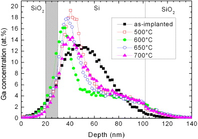
Figure 1. Ga concentration depth profiles in the SiO2/Si/SiO2 film stack obtained from RBS measurements. Annealing for 60 s at temperatures given in the legend causes Ga accumulation at the upper SiO2/Si interface. Interface mixing due to Ga implantation is indicated by the gray region.
Download figure:
Standard image High-resolution imageThe evolution of the layer morphology with increasing annealing temperature is shown in figure 2 (upper row) as a gallery of cross-sectional bright-field TEM (BF-TEM) images. From top to bottom in the images one can clearly discriminate the layer sequence of deposited SiO2 film, Si:Ga film and thermally grown SiO2 layer. In the as-implanted state, the Si layer is 78 nm thick and completely amorphous as indicated by the Fourier-transform pattern depicted as inset. The initially amorphous Si layer becomes nanocrystalline after annealing. Typical sizes of the randomly oriented Si grains are in the range from 5 to 20 nm with the tendency of coarsening with increasing annealing temperature. There is no indication for crystalline impurity phases from the Fourier transform of the corresponding high-resolution (HR) TEM images of the Si:Ga layer. However, the HRTEM micrographs (not shown here) reveal some amorphous inclusions which survive even at the highest annealing temperature. A high Ga concentration is detected in the amorphous regions by EDXS. However, quantitative determination of the Ga content is not possible because the spectra include Si signals from the crystalline environment of the Ga-rich amorphous regions.

Figure 2. Sequence of cross-sectional BF-TEM images (top row) and HAADF-STEM images (bottom row) showing the morphology of the film stack in the as-implanted state and after annealing at various temperatures. The Fourier transforms of the corresponding high-resolution TEM data of the Si:Ga films (FT insets) correspond to amorphous and nanocrystalline Si for the as-implanted and annealed states, respectively. The HAADF-STEM images illustrate the presence of Ga-rich precipitates (bright regions). The film annealed at 600 °C is superconducting, whereas all other films are insulating.
Download figure:
Standard image High-resolution imageUnder equilibrium conditions Ga and Si are almost immiscible [28]. The maximum equilibrium solid solubility amounts to about 0.1 at.%. Therefore, the formation of pure metallic Ga precipitates appears possible during annealing. Since Ga has a low melting point of about 30 °C and as nanoparticle exhibits an extreme undercooling [29], liquid droplets could exist in the Si matrix under the conditions of the TEM analysis. At low temperatures, Ga should crystallize in a variety of allotropes [28]. Cross-sectional TEM investigations performed at temperatures down to 90 K demonstrated that the Ga-rich regions remain amorphous and the layer morphology stays unchanged. Thus, one can suppose that the amorphous regions represent a metastable, amorphous Ga–Si mixture. However, a substructure of these regions below the nm scale is difficult to resolve. For example, a dense cloud of sub-nm Ga clusters dispersed in nanocrystalline Si would mimic an amorphous state.
Whereas the BF-TEM micrographs (figure 2, top row) show both, mass-thickness and diffraction contrast, HAADF-STEM images predominantly exhibit atomic number contrast. In figure 2 (bottom row), HAADF-STEM images of equivalent regions as shown in figure 2 (upper row) are compiled. Bright areas are related to higher atomic number and, therefore, can be associated with Ga-rich regions. In the as-implanted state, the gradual vertical contrast change is correlated with the implantation profile of Ga. The lateral mass homogeneity is lost after annealing and Ga-rich inclusions are formed. They are distributed over the whole film but accumulate beneath the capping layer as already indicated by RBS. The direct comparison of the BF-TEM with the HAADF-STEM images confirms that the Ga-rich regions are the amorphous ones. The Ga-rich inclusions in the interface band do not percolate and their separation increases with annealing temperature. Typical gaps between the nanoinclusions in the interface area vary between 3 and 20 nm for annealing at 500 and 700 °C, respectively. The mean inclusion size increases with annealing temperature from about 4 to 7 nm, whereas the inclusion density decreases. Comparing the data of RBS and the image analysis, one can estimate that the amorphous nanoinclusions should contain more than 30 at.% Ga.
3.2. Transport properties
For transport measurements, samples were patterned in VdP or HB structures [30]. The sheet resistance of the VdP samples in the as-implanted state and annealed at various temperatures is shown as a function of measurement temperature in figure 3. The as-implanted sample is highly resistive (78 MΩ at 300 K). In agreement with recent results [24] indicating a sheet resistance of about 13 kΩ separating superconducting from insulating Si:Ga layers, only the sample annealed at 600 °C (R = 1.3 kΩ at 300 K) becomes superconducting below 7 K. The other samples (R > 24 kΩ at 300 K) behave insulating with strongly increasing resistances at low temperatures. As shown in figure 4, the sheet resistance curves can be fitted in a wide range of temperatures (7 K < T < TES ∼ 200 K) by R = R0 exp[(T0/T)1/2]. This behavior is typical for disordered systems such as heavily doped semiconductors, where variable-range hopping in a narrow impurity band with Coulomb gap (Efros–Shklovskii (ES) hopping) [31] takes place as well as for granular materials in which the transport is governed by the interplay between tunneling through barriers and blocking due to the charging energy of metallic grains [15, 16, 32–35]. Both mechanisms could be active in the Ga-enriched Si films, because metallic Ga-rich nanoinclusions are embedded in a degenerately doped Si matrix.
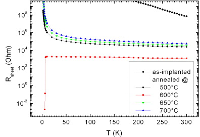
Figure 3. Temperature dependence of the sheet resistance of VdP samples in the as-implanted state or annealed at different temperatures for 60 s.
Download figure:
Standard image High-resolution image
Figure 4. Plot of the sheet resistances shown in figure 3 as a function of T−1/2 illustrating the ES hopping characteristics of the transport in the insulating samples (solid symbols). The open symbols are data from a second measurement in the temperature range from 3 to 12 K demonstrating the reproducibility of the transport behavior. Kinks in the resistance curves at the critical temperature are indicated by arrows. Thin black and thick red lines are fits according to hopping or Arrhenius-type transport, respectively.
Download figure:
Standard image High-resolution imageThe upper limit of the charging energy EC [15] can be estimated when considering the dielectric constant of silicon (εr = 12) as the minimum value in the film. We obtain EC < 60 meV or 8 meV in dependence of the nanoinclusion size that ranges from 2 to 15 nm. In fact, such high-energy barriers would block most of uncorrelated hopping events at low temperatures. Even if we assume that due to heavy doping εr could be ten times larger the lowest barrier of 0.8 meV is still sufficient to suppress sequential tunneling below 30 K. However, Coulomb blocking can be circumvented by inelastic co-tunneling [15, 32]. In this case, cooperative hop-in–hop-out processes allow for charge transport over distances of several particles without charging intermediate particles. The temperature below which inelastic co-tunneling prevails against sequential tunneling can be estimated by Tinel > 2.8EC/kB [32]. Since Tinel ⩽ TES = 200 K, we arrive at EC < 6 meV for the mean barrier in reasonable agreement with the results above.
Between 6 and 7 K anomalies such as little kinks or even hystereses have been observed in several measurements of insulating samples. Two examples are indicated by arrows in figure 4. The coincidence of this temperature range with the critical temperature of superconductivity in the sample annealed at 600 °C implies a sudden change of the transport properties likely due to local superconducting transitions even in the insulating samples. Probably the Ga-rich nanoinclusions shown in figure 2 become superconducting in this temperature range. Similar critical temperatures have been observed for nm-sized Ga inclusions in GaAs and GaP [36] as well as for Ga confined in nanoporous glasses [37]. Below the critical temperature of the superconducting transition, the resistance curves of the insulating samples annealed at 650 or 700 °C start to deviate from the hopping law. The resistance becomes larger than extrapolated from the high-temperature data. Similar results have been obtained e.g. in granular metals [38–41] and TiN films [42]. At the first glance, these results are counterintuitive, because in the simple model of a random resistor network, frequently used to describe the transport in disordered systems [31], the onset of superconductivity in the metal-rich inclusions should lead to a lower sheet resistance. In order to understand this paradox, one has to consider that now the network consists of Josephson junctions instead of resistors [43]. In addition to Cooper-pair tunneling through these junctions, inelastic co-tunneling of quasiparticles contribute to the electrical transport [15, 32]. However, the quasiparticle density in the inclusions diminishes by Cooper pairing as ∼ exp(− Δ/T) when the superconducting gap Δ opens with decreasing temperature T [17]. Because the Josephson current is suppressed by fluctuations [44] when the normal-state resistance of the junction exceeds the critical value, an Arrhenius-type resistance growth is expected below the critical temperature [17]. This is just what we found in our experiments (see the thick red lines in figure 4).
Key parameters for the control and understanding of the electrical transport in materials are the type, concentration and mobility of charge carriers which can be determined by Hall-effect measurements [30]. In the simplest model, the type of the carriers is given by the sign of the Hall-coefficient, RH, and their concentration by c = (eRH)−1, with e the elementary charge. This simple interpretation breaks down for materials with complex band structure or heavy disorder. However, in the case of disordered materials with high carrier concentration such as degenerately doped semiconductors [45] or granular metals [46, 47] the Hall-coefficient provides an effective concentration, c* = Ac, that differs from the real one only by a numerical factor A ⩽ 1. Therefore, the Hall-effect measurement of the Si:Ga films should yield reliable data on the carrier type and the temperature dependence of the carrier concentration in the normal state. The temperature dependence of the effective sheet carrier concentration, (eRH)−1, of the insulating samples is shown in figure 5. All insulating samples exhibit p-type conductivity as expected for Ga-doped Si and an almost constant carrier concentration from room temperature down to 30 K. Assuming a box-like carrier profile over the film width of 80 nm, the volume hole concentration is larger than 3 × 1019 cm−3 which exceeds the threshold of ∼ 2 × 1019 cm−3 for the MIT in Si:Ga [48]. In the case that most of the carriers were located in the Ga-rich film at the interface, the volume concentration would increase by a factor of 5–8. Indeed, the temperature-independent carrier concentration of the insulating samples found for temperatures above 30 K is characteristic for metals. However, the transport is hampered by carrier localization due to heavy disorder in the films. Therefore, the hole mobility is low (< 1 cm2 V−1 s−1) and the sheet resistance has a hopping-like temperature dependence (see figure 4). The Hall-effect data of the superconducting sample are very noisy, partly changing sign, because the Hall-voltage is in the range of the experimental resolution. From this limit it can be estimated that the carrier concentration must be larger than 1 × 1021 cm−3. Consequently, the origin of the lower normal-state resistance of the superconducting sample is a carrier-concentration effect alone and the carrier mobility is as low as in the insulating samples (see supplementary figure S2, available at stacks.iop.org/NJP/15/083022/mmedia).
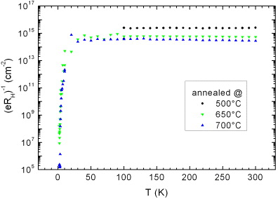
Figure 5. Effective sheet carrier concentration, c* = (eRH)−1, of the insulating samples as a function of temperature determined by Hall-effect measurements at B = 1 T. The Hall-effect data of the sample annealed at 500 ° become noisy below 100 K and, therefore, are not shown.
Download figure:
Standard image High-resolution imageBelow 10 K, the Hall-effect data of the insulating films reflect a carrier freeze out with an activation energy of about 4 meV which is of the same order as the superconducting gap 2Δ = 2.64 meV [23]. This effect supports the idea that the formation of Cooper pairs captured in Ga-rich inclusions is the reason for the Arrhenius-type resistance increase below the critical temperature.
For the SIT, two fundamental different models have been discussed in the literature [17]. In the bosonic model, the Cooper-pair condensate can undergo a quantum phase transition from the superconducting to an insulating ground state depending on a control parameter (e.g. disorder or external fields). Alternatively, the SIT can also occur when Cooper pairs break due the weakening of the pairing forces and the quasiparticles become localized by high electron–electron correlation or disorder. This is the so-called fermionic scenario. In our insulating films Cooper pairs remain trapped in the nanoinclusions and quasiparticle co-tunneling between them determines the transport at temperatures below TC. Thus, an insulating state with a global bosonic condensate can be excluded. This result is corroborated when one compares the relevant energy scales describing granular superconductors. The Josephson-coupling energy can be calculated by use of EJ = 3227 Ω Δ/R [15]. When we take the normal-state sheet resistance at 10 K as a rough approximation for the intergranular resistance R at low temperatures, the Josephson coupling energy is smaller than 4 μeV in the insulating samples. This means EJ ≪ EC and a global condensate cannot be formed. The main reason for the high intergranular resistance is the combination of incomplete acceptor activation and high disorder in the films as revealed by the Hall-effect analysis. Thus, the influence of localization due to electron–electron correlation or quantum interferences on the intergranular resistance as e.g. discussed in [15] should be much smaller in the insulating films than activation and disorder effects.
In the superconducting sample EJ amounts to about 2 meV which is still lower than the 6 meV estimated as upper limit of the mean charging energy. Assuming a higher dielectric constant [16] one can easily fulfill the energetic condition EJ > EC for the coherent coupling of the local condensates. Moreover, one should consider that our films are not granular materials in the strict sense—metallic particles with a thin insulating shell. Therefore, approaches based on that model can be too crude for a quantitative description. For instance, the size of superconducting puddles can extend the nanoinclusion size due to the proximity effect in the doped semiconductor matrix. In this context, it is interesting to check whether the classical Anderson criterion for superconducting nanoparticles, namely that the mean level spacing in the particle δ ∼ V/D (with V the particle volume and D the density of states) must be smaller than the superconducting gap Δ, holds even for the Ga-rich nanoinclusions in Si:Ga. As a consequence of this condition only particles larger than the minimum size dmin ∼ (ΔD)−1/3 can become superconducting. For the free electron gas the mean density of states D = 2.7 × 10²¹ eV−1 cm−3 (n/1021 cm−3)1/3 is a function of the charge-carrier concentration n. Assuming further that n is at least as high as the effective carrier concentration determined by the Hall-effect measurements, we estimate as upper limits dmin = 9.1 nm for the nanoinclusions in the insulating sample with the highest resistance (annealed at 700 °C) and dmin = 6.5 nm in the superconducting sample. These upper limit values fall just in the size range of the Ga-rich inclusions from 2 to about 15 nm. Thus, the Anderson criterion is fulfilled at least for part of the nanoinclusions.
With respect to a possible application of superconducting Si:Ga films in devices, one has to check the stability of the condensate and the film properties under electrical operation (for the effect of magnetic field, see supplementary figures S5 and S6, available at stacks.iop.org/NJP/15/083022/mmedia). The critical current for the superconducting transition as a function of temperature is shown in figure 6 (see supplementary figure S3). The value of 1 mA at 3 K measured at a HB structure corresponds to a current density of 2 kA cm−2. Although such currents applied at temperatures below 30 K do not modify the film properties, irreversible changes have been obtained at higher temperatures. We found that superconducting Si:Ga samples can lose their zero-resistance state and then demonstrate quasi-reentrant superconductivity. Such a quasi-reentrant behavior is known from granular metal films [17–19] and networks of Josephson junctions [49]. In order to study these current-induced modifications, two samples, one with complete superconducting transition (#1) and the other with quasi-reentrant behavior (#2), were subjected to 10 s current pulses of 1 mA at 300 K. The sheet resistance of these samples was measured as a function of temperature using an excitation current of 1 μA (see figure 7). Obviously, the current pulses can increase the normal-state resistance by more than one order of magnitude and drive Si:Ga films from the superconducting into a quasi-reentrant or even into an insulating state. It can be supposed that the resistance increase is a consequence of structural changes in the Ga-rich film caused by electromigration of Ga or current-induced defects in the interface region [50]. The kind of structural changes is still unknown, but one can guess that high currents cause separation and coarsening of the Ga-rich inclusions. Thus, it has a similar effect as thermal annealing.

Figure 6. The critical current of a superconducting HB sample as a function of temperature. The solid line is a guide to the eyes.
Download figure:
Standard image High-resolution image
Figure 7. Irreversible modification of the sheet resistance of two samples (#1, #2) by current pulses of 1 mA for 10 s applied at 300 K. Quasi-reentrant behavior is obtained after current stress. The stress time given in the figure is the sum of the pulse times.
Download figure:
Standard image High-resolution imageThe impact of high currents on the low-temperature electrical transport has been investigated on a HB sample exhibiting an incomplete superconducting transition. The resistance measurements started with a current of 1 μA and were then repeated with higher currents. This measurement cycle was performed four times demonstrating the reversibility of the current effect. The results are shown in figure 8. Obviously, there is a strong effect of the current on the low-temperature transport. A quasi-reentrant behavior is found for 1 μA which is weakened with increasing current up to 100 μA. This behavior is anomalous in that sense that high currents should degrade the superconducting transition as observed e.g. in granular high-temperature superconductors [51, 52]. However, this argument is only valid for currents close to the critical one which is in our case about 1 mA. By applying the critical current, Cooper-pair formation is completely suppressed and the resistance becomes almost independent of temperature. Thus, one can conclude that the deviations from the normal-state resistance are quantum effects appearing in disordered superconductors even above the critical temperature [53]. Due to these quantum effects, the current–voltage characteristics become nonlinear and the resistances behave non-monotonic with excitation current [20, 53–56] (see supplementary figure S4, available at stacks.iop.org/NJP/15/083022/mmedia).

Figure 8. Reversible current effect on the sheet resistance and the superconducting transition. The sheet resistance was measured four times with the following sequence of excitation currents: 1, 10, 100 μA and 1 mA. Only the results of the first run (full symbols) and the last run (open symbols) are shown. Subsequently, further measurements with excitation currents in the range from 50 to 500 μA were performed. The results for 350 and 500 μA are shown as gray lines. Note the non-monotonic behavior of the sheet resistance with excitation current below the critical temperature.
Download figure:
Standard image High-resolution image
4. Conclusions
Ga-rich Si films (∼ 80 nm) sandwiched between SiO2 substrate and thin SiO2 cover layer (∼ 30 nm) have been fabricated by high-fluence Ga implantation and subsequent RTA. The morphology and the electronic transport properties of these films have been studied.
In all of the annealed samples, Ga accumulates in a narrow band (∼ 15 nm) beneath the SiO2 cover layer with laterally averaged peak concentrations of up to 19 at.% Ga. The band consists of an array of amorphous nanoinclusions with Ga content higher than 30 at.% embedded in a nanocrystalline Si matrix. Although the density of Ga-rich nanoinclusions is high in this band, no direct percolation is observed. Both, the mean inclusion size and the gaps between them, grow with increasing annealing temperature. Thus, the Ga-rich inclusions form a random network of junctions to degenerately doped Si crystallites. Little changes in the junction properties can cause phase transitions in the electronic transport.
In the normal state, the electrical transport is governed by ES hopping of holes available in concentrations higher than necessary for the MIT. Below the critical temperature of about 7 K, the Ga-rich nanoinclusions become superconducting. However, in dependence of the normal-state resistance, the local superconducting condensates can couple or not, with the consequence that Si:Ga films behave superconducting or insulating. In agreement with the literature, we found that the critical resistance is less than 24 kΩ. The sheet resistance is a non-monotonic function of the annealing temperature with a minimum value for annealing at 600 °C. It is mainly determined by the effective hole concentration and, therefore, by Ga-acceptor activation attained after annealing.
The sheet resistance can also be modified by current pulses applied at room temperature. It is possible to gradually change the low-temperature transport properties of the Si:Ga film from the superconducting over quasi-reentrant to insulating state. In addition to this irreversible change, the superconducting transition can be reversibly controlled by current variation at low temperatures.
In conclusion, Si:Ga films show a wealth of transport phenomena which have been known until now only from granular metals or high-temperature superconductors. The possibility to fabricate and tailor Ga-rich Si films with microelectronics-compatible technology makes them interesting for both fundamental research on transport phenomena in nanostructured, disordered superconductors as well as for the integration of superconducting circuits into Si devices.
Acknowledgment
Part of this work was supported by DFG (contract no. HE 2604/7-1).