
Abstract
In this work, we review recent progress achieved in the use of chemical solution deposition (CSD) based on fluorinated metalorganic precursors to grow superconducting REBa2Cu3O7 (REBCO) films and coated conductors (CCs). We examine, first of all, the advances in optimizing the steps related to the solutions preparation, deposition and pyrolysis based on novel low-fluorine metalorganic solutions. We show that a new type of multifunctional colloidal solutions including preformed nanoparticles (NPs), can be used to introduce artificial pinning centers (APCs). We analyze how to disentangle the complex physico-chemical transformations occurring during the pyrolysis with the purpose of maximizing the film thicknesses. Understanding the nucleation and growth mechanisms is shown to be critical to achieve a fine tuning of the final microstructure, either using the spontaneous segregation or the colloidal solution approaches, and make industrially scalable this process. Advanced nanostructural studies have deeply modified our understanding of the defect structure and its genealogy. It is remarkable the key role played by the high concentration of randomly distributed and oriented BaMO3 (M = Zr, Hf) NPs which enhance the concentration of APCs, such as stacking faults and the associated partial dislocations. Correlating the defect structure with the critical current density Jc(H,T,θ) allows to reach a tight control of the vortex pinning properties and to devise a general scheme of the vortex pinning landscape in the whole H–T phase diagram. We also refer to the outstanding recent achievements in enhancing the vortex pinning strength by shifting the carrier concentration in REBCO films towards the overdoped state, where the pinning energy is maximum and so, record values of critical current densities are achieved. This confirms the performance competitiveness of nanocomposite CCs prepared through the CSD route. We conclude with a short summary of the progress in scaling the CC manufacturing using fluorinated solutions.
Export citation and abstract BibTeX RIS

Original content from this work may be used under the terms of the Creative Commons Attribution 4.0 license. Any further distribution of this work must maintain attribution to the author(s) and the title of the work, journal citation and DOI.
Acronyms as they appear in the article
| HTS | High temperature superconductor |
| REBCO | REBa2Cu3O7 |
| RE | Rare earth or yttrium |
| CC | Coated conductor |
| APC | Artificial pinning center |
| PLD | Pulsed laser deposition |
| MOVCD | Metalorganic chemical vapor deposition |
| RCE-DR | Reactive co-evaporation-deposition and reaction |
| CSD | Chemical solution deposition |
| CAPEX | Capital expenses |
| TLAG | Transient liquid assisted growth |
| SS | Spontaneous segregation |
| STEM | Scanning transmission electron microscopy |
| EELS | Electron energy loss spectroscopy |
| XMCD | X-ray magnetic circular dichroism |
| TFA | Trifluoroacetate |
| BYF | (Ba1−x Yx )F2 + x |
| TEA | Triethanolamine |
| PEG | Polyethylene glycol |
| acac | 2,4-pentanedione |
| BYTO | Ba2YTaO6 |
| BZO | BaZrO3 |
| BHO | BaHfO3 |
| BCO | BaCeO3 |
| BTO | BaTiO3 |
| BSO | BaSnO3 |
| SZO | SrZrO3 |
| BNO | BaNbO3 |
| UTOC | Ultra-thin once-coating |
| PVP | Polyvinylpyrrolidone |
| CTAB | Hexadecyltrimethylammonium bromide |
| Ps-DVB | Poly(styrene-co-divinylbenzene) |
| TREG | Triethylene glycol |
| MW | Microwave |
| SEM | Scanning electron microscopy |
| FIB | Focused ion beam |
| IJP | Ink jet printing |
| OM | Optical microscopy |
| TGA | Thermogravimetric analysis |
| EGA | Evolved gas analysis |
| MS | Mass spectroscopy |
| DTA | Differential thermal analysis |
| DSC | Differential scanning calorimetry |
| OI | Optical interferometry |
| FT-IR | Fourier transformation infra-red |
| TMA | Thermomechanical analysis |
| CTA | Conventional thermal annealing |
| OF | Ba(Fx Oy )2 |
| FH | Flash heating |
| Y225 | Y2Cu2O5 |
| LAO | LaAlO3 |
| CZO | Ce1−x Zrx O2−y |
| YSZ | (Zr,Y)O2−x |
| IBAD | Ion assisted beam deposition |
| ABAD | Alternating beam assisted deposition |
| RABiT | Rolling assisted biaxial texturing |
| HAADF | High angle annular dark field |
| LAADF | Low angle annular dark field |
| EDX | Energy dispersive spectroscopy |
| SQUID | Superconducting quantum interference device |
| SF | Stacking fault |
| TB | Twin boundary |
| APB | Antiphase boundary |
| FFT | Fast Fourier transformation |
| Y123 | YBa2Cu3O7 |
| Y124 (Y248) | YBa2Cu4O8 |
| GPA | Geometric phase analysis |
| MTG | Melt textured growth |
| DFT | Density functional theory |
| NP | Nanoparticle |
| Bi2212 | Bi2Sr2CaCu2O8 |
| OD | Overdoped |
| UD | Underdoped |
1. Introduction and scope
Since the discovery of HTSs there has been an overwhelming interest in developing suitable conductors for the many potential applications where HTS can bring unique or improved functionalities, particularly in power and magnet applications [1]. Several generations of conductors have been examined in the last 30 years which have diverse performances when they work under different conditions of temperature and magnetic field [2, 3]. As a general rule, it has been demonstrated that the HTS conductors achieve excellent performance, and in many cases, such as in magnet applications, they are unique, i.e. there is no other conductor capable of generating the high or ultra-high magnetic fields that HTS conductors can (B > 30 T) [4]. In other cases, HTS conductors lead to very appealing performances but they must compete with other non-superconducting materials to generate competitive devices (cables, motors, etc) [5, 6]. In both cases a figure of merit determines how fast will be the penetration degree of HTS conductors into the market, i.e. the cost/performance ratio which can be measured in terms of €/kA m, where € considers the capital and manufacturing cost for 1 m of conductor when it carries 1 kA of transport current without losses at given conditions of temperature and magnetic field. Of course, the acceptable figure of merit will differ for each application and also the selected working conditions and also other performances will also influence the acceptability of the conductors. Overall, it is clear that the R&D effort must be directed towards reducing this figure of merit as much as possible by reducing the production costs and enhancing the performance (figure 1) [7, 8].

Figure 1. General schema of the combined objectives required to increase the market penetration of coated conductors in power applications and magnets. Reducing the figure of merit cost/performance requires combining two paths: increasing the performance and decreasing the cost. A non-exhaustive list of the most relevant issues to be considered are included which apply for coated conductors processed by chemical solution deposition (CSD), although not all of them are tackled in the review.
Download figure:
Standard image High-resolution imageSince the discovery of suitable methods to grow the REBa2Cu3O7 (RE = rare earth or yttrium; REBCO) HTS phase as epitaxial film on metallic substrates, i.e. the creation of CCs [9], a new avenue for the fabrication of practical conductors based on the HTS materials and having the highest superconducting performance in a very extended range of temperature and magnetic fields was opened. The challenges in terms of materials science were tantalizing, it was never even imagined that kilometric epitaxial films could be produced. However, the progress achieved in the development of high performance CCs has been extraordinary in the last 20 years and now CCs can be considered a reliable industrial product, even if the figure of merit mentioned before still requires further reduction to become widely commercial. In addition, throughput, yield homogeneity and reproducibility require further improvement. Many different CC architectures (metallic substrates, texturing source, buffer layers) and deposition and growth methods of REBCO films have been devised, all of them with some advantages and disadvantages. Overall, impressive efforts have been made to further advance the knowledge to enhance their competitiveness [2, 10, 11].
The second big boost in the enhancement of the CCs performance was the creation of methodologies to prepare nanocomposite films where nanometric secondary phases could be introduced in high concentration. The increase of CC performance at high magnetic fields requires that vortices pin in APCs with dimensions in the range of few nm (∼5–10 nm) with separation in the range of few tens of nm. Additionally, these secondary phases (NPs, nanorods, etc) usually interact with the preexisting defects and so the very challenging objective of controlling the nanostructure of REBCO nanocomposite films was extensively revised.
Among the different successful film growth approaches for nanocomposite CC fabrication we particularly mention PLD [3, 12–14], MOVCD [15, 16], e-beam metal evaporation [17] as procedures where deposition and growth are simultaneous processes, or in short, simultaneous methods. On the other hand, RCE-DR [18] and CSD are growth methodologies where the precursors are first deposited and then reacted to grow the REBCO pristine and nanocomposite films (i.e. sequential deposition and growth approaches, or in short, sequential methods) [10, 19–27] which have also reached very attractive performances. Many reviews have addressed the peculiarities of the various available growth techniques. Most relevant discussed issues were in connection with the demands on materials characteristics, cost and performance requirements, specially from the device developer's side.
In the case of the CSD approach to CCs, although more than 34 years have spanned since the first demonstration of epitaxial YBCO thin films growth on single crystal substrates [19], it was clear from the beginning that the CSD route was very promising but was still in its infancy. Therefore, a huge amount of new knowledge was needed in many areas, such as solution chemistry, materials science, physics and engineering, as well as to disentangle the correlation to the final performances [20, 22, 23, 28–32]. Many different academic and industrial groups have contributed to progress in the knowledge generation about the CSD approach to CCs. Nowadays, this technique has achieved the required degree of maturity for its industrialization. A very significant appeal of CSD, is the low CAPEX required to build a manufacturing unit, owing to the fact that it does not require the use of vacuum systems or complex furnaces. It is also based on relatively common chemicals and so the running expenses are expected to be rather low, however, as it will discussed later, there remains some drawbacks related to the production throughput which limits an extensive commercial penetration. Therefore, the CSD approach to CCs is being considered as a potential competitive manufacturing technique provided that performance, throughput and yield can be enhanced at industrial scale [8].
Owing to the fact that the knowledge about CSD epitaxial film growth was at the lowest level [25, 26, 32–39], as compared to the other more classical thin film growth approaches used to grow CCs, it was required to deeply investigate many aspects of this technique. During the last 11 years an extraordinary progress has been made in the generation of knowledge about different steps of the CSD approach to thin films and CCs (figure 2). This review intends to be a timely overview of the recent progress of this technique [20, 28, 40].

Figure 2. General schema of the different processing steps involved in the chemical solution deposition route to YBa2Cu3O7 films: metalorganic solution preparation, solution deposition, pyrolysis, nucleation and growth of the epitaxial films and oxygenation.
Download figure:
Standard image High-resolution imageThe review is organized in a sequential manner. All the aspects being relevant in the achievement of pristine and nanocomposite REBCO films and CCs are tackled following the steps of the CSD route based on fluorinated precursors. Emphasis is made on the low fluorine metalorganic solutions leading to intermediate oxides and the fluoride precursor BaF2. This route was initiated 34 years ago and it was considered very relevant because the formation of BaCO3 could be avoided as an intermediate phase. At that time, the general belief was that it would become impossible to grow REBCO CCs at a reasonable temperature because BaCO3 was stable at to very high temperatures. Recently, this assumption has been reconsidered and fluorine-free metalorganic precursors have shown to be suitable for CSD routes to CCs, even if BaCO3 is formed as an intermediate compound [41–49]. The fluorine-free approach encompasses completely different growth routes with mechanisms which still require further research to be elucidated [43, 46]. Particularly, it has been recently shown that the so called CSD-TLAG technique benefits from the developments previously made in the conventional fluorinated CSD route to CCs but goes well beyond its practical limitations. The REBCO growth route fully differs because intermediate transient liquids are used to grow the films and so the growth rate can be enhanced by three orders of magnitude [8, 50]. The fluorine-free metalorganic precursors have also been used to fabricate superconducting joints between REBCO CCs [51, 52]. Owing to the fact that the CSD fluorine-free approach is still an emerging field of research we will consider this topic out of the scope of the content of this review.
In section 2, the review concentrates on the new developments related to the preparation of low fluorine metalorganic solutions which are the starting point for any CSD REBCO thin film growth, as well as in the synthesis of oxide NPs through high throughput chemical methods and their stabilization into colloidal multifunctional solutions. In this section we review as well the advances on the complex preparation of thick films by a single deposition, mainly using in-situ analysis of the pyrolysis stage. The issue of the nanoscale film homogeneity is envisaged in relationship with the intermediate phases evolution during the heating process.
Section 3 is mainly devoted to the analysis of the nucleation and growth mechanisms of the epitaxial REBCO films, either pristine or nanocomposite. First, the in-situ study of the film growth rate of pristine films at different temperatures is presented and then the mechanisms to control the supersaturation degree in thick film are described.
The most significant part of section 3, however, focuses on the progress in understanding the growth mechanisms of nanocomposite REBCO films. We first review the case of the SS route where the NPs and the REBCO films grow from the same solutions. A second, more innovative approach, is to use the multifunctional inks described in section 2 to grow films. This approach is novel in the broad field of oxide nanocomposite processing by means of CSD and so extensive analyses are presented of the different phases and complex phenomena. Overall, we show that this new type of multifunctional colloidal inks is a very attractive tool for a very competitive industrial route to CSD CCs.
In section 4 we report on the advances in the control of the nanostructure of the nanocomposite films and its correlation with the superconducting critical currents. First, we include an overview of how the self-field percolating currents can be reduced due to existing defects or secondary phases and how this effect can be minimized. Additional important content of this section is a summary of the advances in understanding the nanoscale structure of pristine and nanocomposite REBCO films grown by CSD. A wide spectrum of defects is described, based on studies made with advanced transition electron microscopy (mainly STEM-EELS) and complemented with the insights of other complementary techniques available in synchrotron radiation facilities, such as XMCD, to detect tiny magnetic moments in specific atomic positions. A great deal of effort has been made during years to clarify how the vortex pinning landscape can be described and controlled to optimize critical currents in different regions of the magnetic phase diagram. In this section an overview of the most relevant advances in this topic is made. Finally, we close section 4 with a summary of the recent advances in enhancing vortex pinning strength following the strategy of increasing the charge carrier concentration by positioning REBCO CCs in the OD state, where the condensation energy is enhanced and consequently the vortex pinning energy is increased. We also include a short summary of the progress on the use of fluorinated solutions to prepare CCs at the industrial scale to produce long length conductors.
We conclude with section 5 where several general remarks are made, including an outlook on the future of CSD routes towards fabrication of CCs.
2. Chemical solutions, NP preparation and colloidal solutions synthesis
2.1. Low fluorine solution synthesis
Preparation of adequate metalorganic precursor solutions is the first step in the route to grow high quality CSD REBCO films. The main requirements are high purity, long term stability and having adequate rheological properties for the specific deposition process to be used. Also good control of the metals stoichiometry is desired to tune the growth properties and/or the superconducting performance. Since the late 80s it was shown that TFA metal salts were promising precursors specially because they led to BaF2 as an intermediate precursor [19]. In recent years, however, it was noticed that the fluorine content of the metalorganic solutions could be strongly reduced without essential modifications of the YBCO film growth mechanism. The reduction of fluorine in the precursor salts has been the most relevant progress in the design of solutions using the BaF2 process and, as it will be shown here and in next sections, several practical advantages have been demonstrated, besides the more obvious environmental interest of reducing the potential hazardous nature of fluorine derivative exhaust gases.
Systematic analyses of low fluorine solutions were presented by several authors [53–57]. For instance, in [54] the influence of starting salts, solvents and additives were tested. Early investigation of the intermediate phases formed after the TFA precursor pyrolysis showed that, when full TFA salts are used, the intermediate precursor containing fluorine after pyrolysis was (Ba1−x Yx )F2 + x (x ⩽ 0.3) (BYF), which means that the total initial F content can be strongly reduced. In [54] it was concluded that the F content could be reduced down to 10% versus the all fluorine content, i.e. a ratio F:Ba of 2:1 could be used which implies that only BaF2 is formed after pyrolysis. The low fluorine solutions have been investigated by several authors demonstrating that excellent superconducting properties can be achieved [53–55, 58–62]. The introduction of fluorine in the solutions could be performed through several salts. For instance, using YTFA salts as the only source of fluorine, and fluorine-free metalorganic precursors for Ba and Cu which are then dissolved in methanol-propionic acid containing a specific amount of TFAH to generate BaF2 after pyrolysis [54]. Another approach uses the minimum amount of BaTFA required to generate BaF2 after pyrolysis mixed with acetates as salts of all the remaining metals [54, 55, 58, 59]. In some cases, the initial acetate metal salts were then converted to propionates. Other used precursors are Cu-2 ethylhexanoate, octyllic acid or Cu–naphtanate salts [53, 57, 63]. Several solute mixtures and additives were investigated to enhance the metal solubility and tune the rheological properties of the solutions with the purpose of generating homogeneous and thick films after pyrolysis. TEA was one of the best choices as additive owing to the well-known stabilization effect as a ligand of Cu complexes [54, 64], however, its content in the solution should be strictly limited to avoid an excessive increase of the solution viscosity which then would increase the film thickness to values where crack formation during the pyrolysis would be unavoidable. Other additives which have been tested are acetylacetone [64–66] and PEG [67] or also AgTFA salts which are known to decrease the nucleation temperature of YBCO films [68–71]. An additional advantage of using low fluorine precursor solutions is that water absorption is strongly reduced during deposition or manipulation of the solution [54, 72, 73] if acac additives are included in the initial solution [64]. This is believed to be due to the existence of coordination compounds (TEA, propionic acid, acac) with the metal salts which consequently prevents their coordination with water molecules. The detrimental effects of high water content in REBCO solutions is widely known, because they lead to inhomogeneous pyrolyzed films. Therefore, to keep a tight control of water content is a critical issue to achieve high reproducibility and high superconducting performance [54, 64, 70].
Concerning the initial metal composition of the pristine YBCO solutions, we should note that several modifications of the stoichiometric Y:Ba:Cu ratios have been reported to tune the growth properties and superconducting performance. We should particularly mention the case of a reduced Y:Ba ratio down to 1:1.5, instead of the stoichiometric 1:2 value in both thin films and CCs. The main consequence of this reduced ratio is that the YBCO growth temperature is decreased and the superconducting properties improved due to the modified microstructure [31, 53, 57, 74–77]. Microstructural studies have shown that these non-stoichiometric compounds display a reduced porosity and a lower concentration of a/b nucleated crystals while the expected secondary phases (mainly Y2Cu2O5 and CuO) do not perturb in a relevant way the epitaxial microstructure and so this modified metal stoichiometry has been widely used by many authors to grow CCs displaying very good superconducting performance [57, 74, 76, 78–81]. It is also worth to mention that the validity of the TFA approach has been widely proved for most of the Rare Earth compounds in REBCO films where high superconducting performances have been demonstrated [40, 73, 82]. In addition, evidence of a systematic evolution of properties and epitaxy development with the RE size was reported [82–84].
Besides the progress in the preparation of pristine solutions for CSD growth of REBCO films, a great deal of work has also been performed in recent years to prepare more complex solutions envisioned for the generation of REBCO nanocomposite films. The first demonstration of nanocomposite CSD films was made using excess of RE2O3 oxides in the solution which then remained in the grown film as NPs [85]. A more successful approach was made by adding Zr or Hf salts (acetylacetonates, naphtenates) and Ba salts excess to form BaMO3 (M = Zr, Hf) NPs through a SS process of NPs displaying a homogeneous nucleation occurring at lower temperatures than the REBCO epitaxial nucleation and growth [20, 22, 23, 40, 73, 86–88]. The solution preparation in these cases was quite straightforward and most of the rules applying to pristine solutions were also valid in these more complex compositions. Other NP compositions were also demonstrated, such as the double perovskites Ba2YTaO6 (BYTO) [89, 90]. In this case, the metal precursors for Ta were tantalum (V) ethoxide while Ba, Y and Cu precursors were TFA salts. NPs concentrations in the final YBCO layer up to ∼15% (mol) were demonstrated, similar to other BaMO3 perovskites. This evidenced that similar compositions, widely investigated in PLD and MOCVD YBCO nanocomposite films, could be prepared and analyzed with the particular microstructure of CSD nanocomposite films [22, 23, 40, 73].
In conclusion, a thorough knowledge advancement related to define the routes to prepare chemical solutions suitable for the preparation of high quality and high performance pristine and nanocomposite REBCO films through the BaF2 route was achieved. The improved robustness, reproducibility and control of the solutions using cost-effective salt precursors, solvents and additives is a definitive boost of the competitiveness of the CSD route to CCs.
2.2. NP preparation and colloidal solution stabilization
Nanocomposite film growth by CSD based on SS of the secondary phases was the first demonstration that nanomaterials could be prepared by this route with very appealing superconducting performances. However, it was shown by several authors that the approach presents several intrinsic limitations related to the control of the size, distribution and homogeneity of the NPs. It was shown that above a concentration of 10%–12% mol in the final YBCO layer there was a tendency towards NP aggregation and the size control of the NPs was compromised [90, 91]. An alternative deposition approach was devised which hindered the NP diffusion and coarsening by taking advantage of the CuO interlayer formed at the intersurfaces of multideposited pyrolyzed films, called UTOC [40, 79–81]. This novel process selects ultrathin (∼30 nm) YBCO layers and a solution multideposition approach to reach competitive total film thickness and critical currents, for instance, 35 repetitions of the spin-coating/pyrolysis cycle were required to get a final film thickness of ∼0.6–0.7 μm [40, 92]. As we will see, the results obtained with this approach are very attractive to achieve very small embedded NPs at the end of the growth process and so high superconducting performances. On the other hand, although the multideposition approach may seem cumbersome, it can be efficiently overcome at industrial scale using automated multilane furnaces and so thick REBCO layers can be easily prepared [93].
Taking into account the practical limitations of the SS approach, a new route to CSD nanocomposites has been explored, never devised before in any type of functional oxides: the multifunctional colloidal solution approach. The main innovation of this route was to prepare separately the selected NPs with a well-defined size, composition and structure through a chemical approach allowing to stabilize them as a colloidal solution. This new colloidal solution has a multifunctional character because it leads to a superconducting YBCO matrix where NPs having other functionalities (insulating, metallic, magnetic) are embedded. Needless to say, many practical difficulties were encountered to reach the desired functional properties, as it will be described in more detail in next sections. Here we will summarize the different approaches which were followed to prepare NP solutions with the desired characteristics of NP size, concentration, distribution and with a long term stability. We should remind that in nanocomposite superconductors the secondary phases should behave as APC, therefore the optimal size of the NPs should be in the range of 2–3 times the superconducting coherence length of the HTSs (d = 5–10 nm). It is also very relevant that the colloidal solution is based on highly polar solvents, mainly alcohols and carboxylic acids, that the NP concentration in the colloidal solution is in the range of ∼12%–25% mol, that the solution remains stable for months, that the NPs keep their composition stable, i.e. they do not react with the YBCO salts, and, finally, that they keep their size (no coarsening) during the following thermal treatments to grow the epitaxial YBCO thin films.
Several oxide NPs were investigated using the multifunctional colloidal solution strategy to prepare YBCO nanocomposites by CSD using the fluorinated solutions [94–96]. After a first trial using metallic NPs, such as Au, the first oxide NPs investigated were the ferrimagnetic spinel ferrites MFe2O4 (M = Mn, Co) which were already available close to the required size [97, 98]. Unfortunately, it was found that these NPs have a strong chemical reactivity with the YBCO precursors and so other simple oxides were investigated, such as CeO2, ZrO2 and HfO2 with the fluorite structure where an accurate choice of ligands was necessary to avoid the formation of supraparticles [94, 99–102]. Since these latter oxides were found to display some reactivity with the Ba salt, forming BaMO3 (M = Ce, Zr, Hf), it was already demonstrated that they enhance the superconducting properties, hence opening a new route to generate attractive YBCO nanocomposite films grown by CSD [95, 103–107]. However, owing to the difficulties to control the NPs size and their distribution when some chemical reactivity exists, the route of using non-reactive ternary oxides, such as the BaMO3 (M = Zr, Hf, Ti) perovskites, was explored by several authors [91, 103–106]. This approach was finally successful, thus very competitive multifunctional colloidal solutions to prepare YBCO superconducting nanocomposites are now available fulfilling all the practical requirements mentioned above.
The most outstanding methodologies which have been used up to now to synthesize oxide NPs through chemical methods are: sol–gel precipitation, hydrothermal, solvothermal and micro-emulsions [107–109].
Although sol–gel precipitation [109] and microemulsion technologies [106], are well established synthetic methods to prepare NPs, they were not useful in the discussed case, since they did not allow to prepare high NP concentrations keeping well dispersed solutions.
Hydrothermal and solvothermal approaches are mild temperature, and sometimes high pressure, growth methods which have been widely used to prepare several binary and ternary oxides and they are considered as high throughput methods, therefore, they were the most used methods for the purpose of preparing CSD superconducting nanocomposites at large scale [103, 110, 111]. Hydrothermal growth uses water as solvent at high pressure, usually adding oleic acid as surfactant to keep control of size and dispersibility. Solvothermal method is a non-hydrolytic pathway where alcohols are used as solvents, either under normal pressure conditions or under pressure using an autoclave. The polyol route allows in this case to control the ligand formation and so achieving stable solutions with fairly high concentrations. The control of homogeneous nucleation and growth of the NPs is usually analyzed following the LaMer model [103, 109, 112]. Solvothermal methodologies have been, therefore, the most successful routes to prepare preformed NPs for CSD nanocomposite growth.
When Au metallic NPs were prepared, reduction of Au salts, such as HAuCl4, were used where the NPs were stabilized with citrate ligands. These solutions are then transformed into colloidal solutions using several polymers (PVP; CTAB; Ps-DVB) which can be redispersed in alcohols (methanol, ethanol). The achieved NPs have an adequate size (∼5 nm), however, only low concentrations could be achieved (few mM) and during the YBCO growth process the NPs displayed a strong tendency to migrate to the film surface [113].
Spinel ferrites MFe2O4 (M = Fe, Co, Mn, Ni, Zn) is a class of oxides which have been widely investigated due to their magnetic properties and NPs have been produced through several chemical methods. The use of the polyol route, i.e. a solvothermal method including metal acetylacetonates and TREG or oleylamine as solvents, was found to be a one pot facile synthesis approach leading to stable and well dispersed colloidal solutions in polar media [97, 98]. The NP sizes were in the range of 3–5 nm and they could be transferred to more polar solvents such as alcohols. These colloidal solutions were dispersed and stabilized in the TFA solutions, however, the strong chemical reactivity occurring at high temperatures strongly limited the suitability of these NPs [114].
An additional advance in preparing oxide NPs for CSD nanocomposites was the growth of fluorite NPs, such as ZrO2, HfO2 and CeO2 [94, 99–101, 115, 116]. These compositions had already been used in YBCO nanocomposites grown through PLD, MOCVD and CSD-SS deposition methods [12, 14, 22, 23, 117, 118]. In addition, the synthesis of the ZrO2 NPs was already reported before and so there were guidelines to synthesize them in the desired size through the solvothermal method using different inorganic precursors (ZrCl4), solvents (benzyl alcohol, dibenzyl ether) and heating methods (conventional furnace heating or MW heating) [94, 100]. Individual, aggregate-free colloidal solutions were achieved with sizes in the range 3–8 nm using alcoholic solvents and keeping ligands in apolar solvents. An interesting result was that using MW heating the growth time could be decreased by a factor ∼40, as compared to conventional heating, conserving a high crystallinity [94, 100, 104]. In all cases, however, ligand exchange was necessary to stabilize the solution in alcoholic media through steric or charge effects [94, 95, 102, 103, 115, 116, 119]. A similar route was followed to demonstrate the suitability of CeO2 NPs to achieve colloidal solutions. The synthesis of NPs with sizes in the range of 5–6 nm could be completed by MW heating during ∼10 min and starting from Ce(III) acetylacetonates and TREG, which was later exchanged with decanoic acid, and so leading to stable solutions in alcohols [94]. The mutifunctional colloidal solutions prepared with TFA or low fluorine YBCO solutions including ZrO2 or CeO2 NPs were stable during months and so they were adequate to grow nanocomposite YBCO films by CSD, as it will be described in later sections, even if they were reactive with Ba precursors.
The most successful approach, up to now, to prepare YBCO nanocomposites by CSD using preformed NPs with controlled size, shape and distribution has been the use of the non-reactive compositions of BaMO3 (M = Zr, Hf) perovskites [103, 105, 120]. These ternary oxides led to self-assembled nanostructures in the case of vacuum deposition approaches (PLD, MOCVD), where simultaneous nucleation and growth of both phases occur and strain is the driving force for self-organization in nanorods structures [121–123]. They were also the best compositions demonstrated so far to prepare CSD YBCO nanocomposites using the SS processes, as we have described in previous sections. Therefore, it was very appealing to develop a robust and reliable method to prepare perovskite NP colloidal solutions. Previous works on perovskite oxide NP growth were mainly focused on the ferroelectric BaTiO3 phase, which is unsuitable for YBCO nanocomposites due to the chemical interdiffusion of Ti and Cu in YBCO that reeduces the superconducting transition temperature [124]. Therefore, the main efforts were centered in preparing Zr and Hf perovskite compositions. Initial attempts were made using microemulsion or sol–gel approaches which led to either non-homogeneous dispersions, low solution concentrations or very long reaction times [100, 105, 106]. To go beyond, a hybrid approach was proposed combining sol–gel and solvothermal respective advantages [103] or also a single solvothermal process performed in a MW reactor [105]. In the novel hybrid approach a suspension is first prepared by sol–gel at room temperature during a short time (∼5 min) using metal alkoxyde precursors and Ba(OH)2 and then a milky solution is obtained by adding TEG and NH3. This solution is then transferred either into a steel autoclave during 1 h or into a MW reactor during a much shorter time (∼5 min) and heated at 180 °C in both cases. The resulting colloidal solutions were finally cleaned through a very specific procedure and dispersed into absolute ethanol, thus being suitable for the preparation of the multifunctional colloidal solution [103]. The use of a single solvothermal step also allows to prepare well crystallized NPs, although with a reduced control of the nucleation step [105] (figure 3).
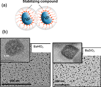
Figure 3. (a) Schema of stabilized oxide nanoparticles prepared for being used to prepare colloidal solutions; (b) TEM images of BMO (M = Zr, Hf) nanoparticles prepared through a solvothermal methodology. Reproduced with permission from [103].
Download figure:
Standard image High-resolution imageIn summary, the knowledge generated on the reaction paths, nucleation and growth mechanisms of the NPs synthesis methods enabled to tune accurately the size and size distribution of NPs [103]. Consequently, a large scale production process for the most successful perovskite cases was devised and can be widely used in long length production of CCs based on CSD [91, 105]. The use of adequate ligands enables long term stability and high concentrations (∼20% mol) of the desired NPs in the REBCO layers.
2.3. Solution deposition and pyrolysis analysis
A key step in the development of high quality CSD thin films and CCs is the solution deposition and the corresponding pyrolysis step. At this stage the metalorganic precursors are decomposed generating a porous nanocrystalline layer where the solid precursors to grow YBCO films should keep the maximum nanoscale homogeneity, and a strict control of the residual porosity is critical to enable a fast gas diffusion afterwards. Thorough analytical studies of the correlation between the characteristics of the chemical solutions, the selected deposition methodology (spin coating, dip coating, slot die coating, IJP) and the pyrolysis process have been undertaken for many years. The most suitable inks for each of these deposition methods may differ owing to the modified rheological properties required in each case. Therefore, fine tuning of the final inks is needed to adapt to the selected solution deposition method. Additionally, many unknowns still remained concerning the physico-chemical transformations of the inks before being transformed into stiff films behaving as inorganic precursors of the YBCO films and, therefore, the pyrolysis process deserved further scrutiny [20].
Most of the first analyses of the pyrolysis process were performed in TFA solutions [20, 32], while more recently, a thorough analysis of the physico-chemical transformations of low fluorine precursors for YBCO films were performed which helped to disentangle the most critical steps. The novel knowledge generated was then successfully used to optimize the thermal treatments to increase the film thickness in a single deposition [125, 126]. Other authors also investigated the pyrolysis process in low fluorine precursors for SmBCO thin films (<300 nm thick) with the aim of accelerating the pyrolysis step [127].
The most troubling sources of film inhomogeneities are the morphological defects generated during the pyrolysis step, i.e. film wrinkling and cracking, both being related to the in-plane stress generated during the metalorganic decomposition process due to the film shrinkage (figure 4). These morphological defects have a strong perturbing effect on the current percolation in superconducting films, therefore, it is absolutely critical to ascertain how to avoid them. Actually, the stress control is a very challenging objective widely investigated in many CSD functional oxides [20, 125, 128–130]. The first goal in this analysis is to determine the temperature windows where each physico-chemical phenomenon appears in order to correlate the multiple aspects being involved: thermal, chemical and mechanical.
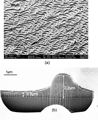
Figure 4. (a) SEM image of a film surface displaying wrinkles after pyrolysis when the film was heated at 15 °C min−1; (b) cross section FIB-SEM micrograph of a wrinkled film. Reproduced from [125]. CC BY 3.0.
Download figure:
Standard image High-resolution imagePrevious analyses of films during the pyrolysis were mainly performed using ex-situ measurements and mainly on thin films (∼200–300 nm) [20, 59, 131–133], however, these ex-situ approaches limit the information about the kinetic aspects of the complex pyrolysis. To go beyond this restrained picture, an investigation combining different experimental tools, most of them working under in-situ conditions, was performed using annealing conditions close to those used in the pyrolysis process. The final film thickness used to perform these in-situ analyses was in the range of 800–1000 nm with low fluorine films deposited by mutideposition spin coating or by IJP in a single deposition. Typical SEM-FIB cross section images of these pyrolyzed films are displayed in figure 5. A fairly homogeneous microstructure is observed in the single deposition films, while those prepared through multideposition display segregated CuO interlayers created during the pyrolysis (figure 5) [20, 36, 40]. The coupled experimental tools used in this study were: in-situ OM including a video recorder, TGA, EGA, MS, DTA, DSC, in-situ OI to determine the film thickness, FT-IR spectra of volatile species and in-situ determination of the viscosity of the films through TMAs [42, 50, 134–137].
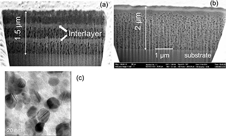
Figure 5. (a) and (b): Scanning electron microscopy (SEM) micrographs of YBCO pyrolyzed films' cross section obtained by focused ion beam (FIB). In (a) 3 coatings with a thickness after pyrolysis of 500 nm were performed by spin coating, showing CuO segregated interlayers. The final film thickness would be around 700–800 nm. (b) Micrograph of a pyrolyzed film with a single coating made by IJP, presenting a fairly homogeneous cross section, except for the formation of a CuO nanolayer at the surface. The final film thickness would be around 1000 nm. (c) TEM image of a pyrolyzed film showing the nanoparticles formed. Reproduced from [125]. CC BY 3.0.
Download figure:
Standard image High-resolution imageThis integrated analysis showed that the pyrolysis process in the low fluorine films differs from that of TFA precursors although it still displays three temperature zones characterized by similar transformations (figure 6): Zone I corresponds to the solution drying region where the solvents are eliminated; Zone II covers the temperature window where wrinkling occurs as a reversible or irreversible phenomenon and the organic precursors start to decompose; Zone III is the region where film cracking occurs and where the transformation of the organic precursors is completed.

Figure 6. Summary of the three different identified temperature regions correlated with the corresponding phenomena. The required temperature ramps are also indicated. (I) Solution drying; (II) reversible or irreversible wrinkling formation; (III) crack formation. The final film thickness would be around 1000 nm. Reproduced from [125]. CC BY 3.0.
Download figure:
Standard image High-resolution imageIn the first zone (T < 150 °C) it was clearly discerned that kinetic effects are not very relevant and so the heating process can be fast (∼20 °C min−1) without any degradation of the film homogeneity. After this stage the film thickness is still in the range of 7 μm for a final film thickness of 700–800 nm. Zone II (150 °C–240 °C) is the scenario, instead, of very relevant transformations. In-situ OM recording shows that depending on film heating rate some wrinkled regions are generated in the film and also that depending on the film composition the wrinkled structure can become reversible. Typically, heating rates in the range of ∼5 °C min−1 are necessary in thick films to avoid permanent wrinkling. TGA and EGA evidenced that in this zone some mass loss already occurs and the composition of the decomposed compounds were identified by FT-IR of the exhaust gases while FT-IR of the remaining films allowed to discern which salts were remaining after decomposing at each temperature [50, 136–138]. It was concluded that the propionate salts decompose in this region while the TFA salts still remain stable in the bonding skeleton of the film (figures 7(a) and (b)). Parallel in-situ determination of the film thickness evolution clarified that the films have a viscoelastic behavior (time dependent thickness evolution) in this temperature range with a limited shrinkage (∼20%–30% film thickness reduction). It was concluded that an in-plane compressive stress develops which lies at the origin of the observed wrinkling phenomena. The film viscosity measurements, additionally, evidenced that the films display a liquid-like behavior in this region and this feature should be at the origin of the observed reversible behavior of the wrinkled structure in some films.
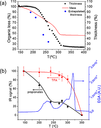
Figure 7. (a) Comparison among mass and thickness evolution during pyrolysis measured by TGA and interferometry, respectively. Film thickness is measured for a film with a final thickness of 700 nm prepared by IJP; (b) comparison of the data obtained from IR spectroscopy and EGA during the pyrolysis of a film deposited with a solution including Y(TFA), Ba and Cu acetates and propionic acid +5% vol DEA as solvent. The blue curve corresponds to the EGA-MS analysis, m/z = 28 (propionates, CO), while the dots, with their guidelines, are the values obtained from the integration of IR bands, black for the integration between 2800–3050 cm−1 (propionates) and red for the bands between 1100–1200 cm−1 (TFA). Reproduced from [125]. CC BY 3.0.
Download figure:
Standard image High-resolution imageThe final temperature zone of the pyrolysis process (zone III) extends from 240 °C to the temperature where the metalorganic decomposition has been completed (T ∼ 320 °C). Within this temperature window, crack formation is occasionally observed by in-situ OM video recording, while FT-IR and TGA show that the remaining metal–TFA bonds are destroyed. Accordingly, significant film shrinkage occurs (∼75% film thickness reduction) generating a strong in-plane tensile stress that can potentially lead to the irreversible formation of macrocracks (figure 8). The previously observed viscous behavior in zone II is progressively lost here when the remaining molecular bonds of the film skeleton are transformed to a stiff nanocrystalline and porous film composed of metal oxides (CuO) and mixed fluorides. It is worth to noting that the prevalence of the remaining TFA bonds in this region plays a crucial role in minimizing the adverse effect of crack formation. Therefore, the kinetics of the process is relevant here and it is advisable to use low heating rates (∼5 °C min−1). It is also worth to remark that heterogeneous nucleation of cracks may be promoted at film impurities and so it is concluded that to achieve homogeneous films is very important (high precursor purity and clean room environment are needed). Also keeping a good film thickness homogeneity during the film deposition and drying is clearly an important issue because, otherwise, the sites of enhanced film thickness may become a crack nucleation center which then propagates along the whole film, as it could be discerned when in-situ OM video recording of the crack formation was made [125] (figure 8).

Figure 8. Typical OM images of IJP films (5 × 5 mm) after pyrolysis and the corresponding thickness maps, as determined by optical interpherometry. (a) Homogeneous film with a final nominal thickness of ∼1100 nm not displaying any crack; (b) corresponding thickness map of the film shown in (a); (c) and (d) pyrolyzed films with a final film thickness of ∼1050 nm showing a few cracks nucleated at the edges of the film. Reproduced from [125]. CC BY 3.0.
Download figure:
Standard image High-resolution imageThe thorough knowledge generated about the physico-chemical transformations occurring during the pyrolysis process has become very useful to maximize the film thickness [139], as well as to accelerate the pyrolysis step [59, 133]. This was demonstrated in an effort to define the best parameters for thick (∼1 μm) film deposition of YBCO films by single deposition IJP to approach the thickest CSD films reached by slot die coating or spin coating by multideposition [29, 126, 140].
IJP has indeed a strong potential as compared to slot die coating for being used as a digital approach of complex material structures, including stripes for low ac losses superconductors, combinatorial screening as a high throughput experimentation technique and so on [127, 141–146]. However, after the first attempts of preparing thick films, it was immediately clear that the composition of the low fluorine solutions and the IJP deposition parameters should be properly optimized to reach a very homogeneous liquid thickness before the pyrolysis process. Concerning the pyrolysis step, similar difficulties appear in IJP as compared to slot die coating or spin coating respect the above mentioned morphological inhomogeneities (wrinkling, cracking) [125, 128, 129, 132, 139]. It is not a trivial goal then to control all the relevant parameters involved in solution deposition by IJP because it is needed to adapt the solutions to the sort of nozzles to be used. For instance, a recent use of machine learning analysis of fluorine-free IJP solution deposition has shown that high throughput experimentation may help to predict the most relevant processing parameters (drop volume, drop pitch, wettability, solvent evaporation rate, etc) [143, 147].
Keeping the liquid layer homogeneous after IJP deposition requires first to redesign the low fluorine YBCO inks in order to avoid the so-called coffee ring effect, i.e. a liquid sucking effect from dried regions of the film. To avoid this effect, the selected strategy was to use solvents with high boiling points (propionic acid and butanol) to avoid evaporation during deposition and preserve the liquid state of the film during the whole deposition process. It was also very beneficial to use small amounts of a photocurable polyacrylic varnish as an ink additive. Then the use of a UV lamp curing process contributed to pin the liquid after deposition and optimize the film thickness homogeneity [126] (figure 9).
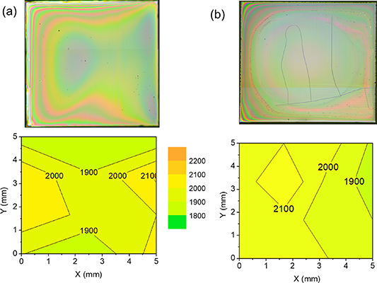
Figure 9. (a) and (b) OM images of IJP films (5 × 5 mm) after pyrolysis and the corresponding thickness maps (in nm), as determined by OI. (a) Homogeneous film with a final nominal thickness of ∼1100 nm not displaying any crack; (b) film with a final thickness of ∼1050 nm showing a few cracks in the central part of the film. Reprinted with permission from [126]. Copyright (2021) American Chemical Society (see also videos S2 and S3 in supporting information).
Download figure:
Standard image High-resolution imageOnce being successful in the goal of keeping a wet high film thickness homogeneity after solution deposition, the optimal heating conditions previously defined in the physico-chemical analysis of the pyrolysis were used. In this way films prepared with a single deposition and a final thickness of ∼1.2 μm could be achieved. These films had typical thicknesses after drying of ∼9 μm and they shrink down to ∼2 μm after the pyrolysis without any film inhomogeneity (figure 9). The performance in terms of film quality of these pristine films could be extended then to the multifunctional colloidal solutions described in the previous section and so thick YBCO nanocomposite CSD films could also be prepared [126, 139]. It is also worth to mention that films thickness in CSD films can be always further increased through multideposition of solutions after an intermediate pyrolysis processes. This multideposition strategy to prepare thick films has been demonstrated by several authors by IJP with thicknesses in the range of ∼1–1.6 μm [126, 127] and by slot die coating with thicknesses in the range of ∼2.5–3.0 μm [29, 31]. In all cases the REBCO growth process of the thick films needed to be reformulated to reach high superconducting performances. Slot die coating has been demonstrated to be a suitable industrial approach to prepare CSD CCs in long lengths when a multideposition approach is used because it can be adapted to a multilane automatized manufacturing system [30, 31, 63, 79, 148–150].
In conclusion, reaching a deep understanding of the chemistry of metalorganic solutions and of colloidal inks to optimize the deposition process is a very relevant goal, whatever deposition technique is used. Afterwards, the use of the detailed knowledge about the physico-chemical transformations occurring during the pyrolysis process for the corresponding chemical precursors is a key issue to optimize the processing conditions.
Needless to say, the deposition and pyrolysis steps can be performed separately from the growth process and so the growth process does not need to be synchronized with the pyrolysis facility. For that reason, minimization of the duration of the deposition–pyrolysis process, though relevant, is not mandatory, contrary to the demand of keeping a high pyrolyzed film quality which is a real requirement to assure high performance after growth.
2.4. Intermediate phase evolution
After the pyrolysis step, an additional relevant process is the nanoscale control of the intermediate solid phases during the heating stage towards the growth temperature. The final reaction leading to the formation of REBCO films in the case of the BaF2 derived processes is a solid–solid reaction controlled by gas diffusion phenomena [20, 21, 28]. Therefore, it is clear that any parameter which may modify the kinetics of this reaction will influence the formation and, very likely, the microstructure of the epitaxial films, including the particular case of the nanocomposite films. Several investigations have been reported in the past concerning the evolution of the intermediate phases during this heating stage. In most of the cases this process is performed under a humid atmosphere and with a fairly low heating rate (∼25 °C min−1) [20, 21, 151, 152]. During this CTA process it has been shown that a deep transformation of the chemical and nanoscale structure occurs. It was shown that the solid solution BYF is transformed to a mixture of an oxyfluoride phase Ba(Fx Oy )2 (OF) and Y2O3 in the early stage of the heating ramp. Sometimes, the existing CuO partially reacts at higher temperatures with the Y2O3 phase forming the intermediate phase Y2Cu2O5 which, actually, competes with the main reaction leading to the direct formation of YBCO (see equations (1)–(3)) [20, 56, 153, 154].
The main reaction leading to the formation of YBCO is:
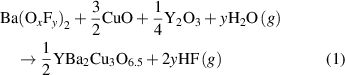
with 0 < y < 1. The intermediate competing reactions with the main reaction (1) are:


Additionally, all the intermediate solid phases display particle coarsening which could even reach, in some cases, particle sizes as big as ∼100 nm (Y2Cu2O5 for instance), thus losing the nanoscale film homogeneity preserved after the pyrolysis process. Needless to say, the nucleation and growth of epitaxial YBCO are influenced by the size evolution of the intermediate phases which then modifies the kinetics of reactions (1)–(3) and the final microstructure.
To minimize the adverse effects of CTA a new heating process was recently devised called FH, where the heating rate is strongly increased to values in the range of hundreds to thousands of °C min−1 (inconstant heating ramp), and so the final heating time is reduced by a factor ∼30 as compared to CTA [152, 155]. The first consequence of using FH is that the initial reactions previously mentioned (BYF transformation, yttria formation) were hindered up to the nucleation and growth temperature of YBCO (∼750 °C–800 °C) and so reactions (1)–(3) occur at a single temperature.
By examining x-ray diffraction patterns of FH films quenched to room temperature after annealing during different times at 810 °C, the evolution of the different crystalline phases could be determined and a kinetic phase diagram could be devised and compared with that obtained with a similar process using the CTA as a heating profile (figures 10 and 11). The first observed modification is that Y3+ ions are expelled from the BYF fluorite phase at higher temperature forming Y2O3 and OF. Immediately after Y3+ ions are expelled from the fluorite structure the competitive reaction (2) leading to Y2Cu2O5 is initiated. However, owing to the short diffusion lengths required to form the new solid phases, the incubation time to nucleate the epitaxial YBCO nuclei was also very short (∼3 min) and so the advancement of the undesirable intermediate reaction forming Y2Cu2O5 is strongly minimized.
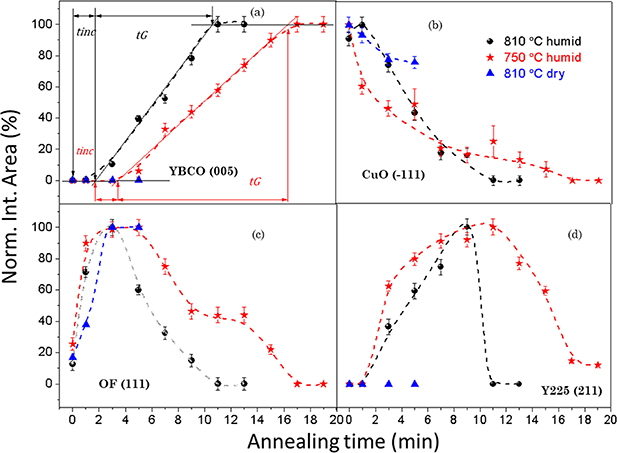
Figure 10. Normalized integrated area dependences with annealing time of x-ray diffraction peaks in a FH process. (a) YBCO(005), where tinc is the incubation time and tG
is the growth time; (b) CuO(−111); (c) OF(111); (d) Y225 (211), respectively, while the samples were quenched at 810 °C in a dry gas atmosphere (blue  ) at 810 °C in a humid gas atmosphere (black
  ) and at 750 °C in a humid gas atmosphere (red
  ) after annealing for selected time periods. Reproduced from [155]. CC BY 3.0.
Download figure:
Standard image High-resolution image
Figure 11. (a) Experimental phase diagram of the intermediate phase evolution in the FH route towards YBCO film formation. The films were heated in a humid atmosphere using the FH process at given temperatures, and quenched after being annealed for different time periods at these specific temperatures. The x-ray diffraction patterns were used to identify the different crystalline phases; (b) corresponding phase diagram of films heated following the conventional thermal annealing approach. Reproduced from [154]. © IOP Publishing Ltd. All rights reserved. Reproduced from [155]. CC BY 3.0.
Download figure:
Standard image High-resolution imageThe second very relevant consequence of FH is that the coarsening of the intermediate NPs is severely restricted and so the nanoscale homogeneity of the precursor films leading to YBCO is strongly enhanced. The increase of the kinetics of reaction (1) leading to YBCO involves the use of the precursor phases (CuO, OF), as it is seen in the fast decrease of the intensity of the corresponding Bragg peaks (figure 10). The main consequence is that the time available to induce some NP coarsening is strongly reduced to less than ∼10 min, i.e. at least one order of magnitude shorter than in CTA films. The estimated coarsening rates of the intermediate phase NPs (CuO, OF, Y2Cu2O5) were in the range 1–4 nm min−1 for the diameter and so their size remains in the range of 5–20 nm, thus strongly enhancing the film homogeneity (figure 12). The observed decrease of the precursors NP size follows the decrease in the Bragg peak intensities (figures 10 and 12) thus indicating that they are consumed to form YBCO. Overall, therefore, the accelerated growth of the YBCO films is facilitated by the enhanced nanoscale homogeneity of the precursor films which reduces the incubation time, even if the growth rate of the YBCO films (⩽0.5 nm s−1) remains similar to those prepared by CTA because the growth mechanism is not modified [152, 153, 156–162].
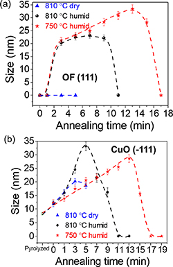
Figure 12. Size evolution of nanocrystalline precursors under different annealing conditions following the FH process: (a) OF, (b) CuO. YBCO thin films are either quenched from 810 °C after heating in a dry gas atmosphere (blue triangle), from 810 °C after heating in a humid gas atmosphere (black sphere) and from 750 °C heating in a humid gas atmosphere (red star). In all cases the nanoparticle size evolution in the FH process can be followed. The nanoparticle size was calculated from the Debye–Scherrer formula using CuO(−111) and OF(111) Bragg peaks. Reproduced from [155]. CC BY 3.0.
Download figure:
Standard image High-resolution imageThe kinetic advantages of the FH process were also found very useful in optimizing the growth of YBCO nanocomposite films through the multifunctional colloidal process described in previous sections. The preformed NPs included in the multifunctional colloidal solutions are always designed to have the optimal sizes for their functionality as APC, therefore, it is desirable that their composition and size are preserved during the processes previous to growth (pyrolysis and heating).
The evolution of the preformed NPs during the whole thermal annealing processes to grow the YBCO nanocomposites was precisely investigated in some particular cases, such as the ferrimagnetic CoFe2O4 NPs, selected as a typical example of oxide system where the magnetic properties are key indicators of their evolution [163]. It was concluded that during the pyrolysis process (T < 310 °C) there is no appreciable NP coarsening.
Summarizing, only the heating process following pyrolysis can influence the NP's size and so special care should be taken to ascertain their stability during the growth in nanocomposite films. Fortunately, as it will be demonstrated in next sections, the ternary perovskite BaMO3 (M = Zr, Hf) NPs displayed a stable behavior (chemical composition and coarsening) when a FH process is used.
In conclusion, a thorough analysis of the intermediate phase evolution during the heating step of the CSD REBCO films from the pyrolysis to the growth temperature has demonstrated that the chemical and microstructural evolution is significant enough to select attractive heating processes, such as FH, which minimize the effects of particle coarsening. Preserving the nanoscale homogeneity facilitates and accelerates the epitaxial growth of the REBCO films.
3. Nucleation and growth of REBCO pristine, nanocomposite films and CCs
3.1. Nucleation, growth and oxygenation of pristine REBCO films and CCs
Understanding the nucleation and growth mechanisms of YBCO epitaxial films prepared through the BaF2 process has been a key objective since the initial efforts to use it as a route to practical applications of films and CCs. It was soon realized that the reaction is based on a solid–solid reaction–diffusion process controlled by gas diffusion which is initiated by a Volmer–Weber type island epitaxial nucleation [20, 28, 35, 164, 165]. Several parameters have been shown to influence the supersaturation degree (total pressure PT , water pressure P(H2O), film thickness, gas flow, ...) and the heterogeneous nucleation (c-axis or ab-axis orientation, nuclei density, strain, RE ion, metal stoichiometry, Ag additives), the growth rate (temperature, PT, P(H2O), PO2), the film strain state (lattice misfit, interfacial defect structure) and the reactivity with the substrate or buffer layer [20, 28, 69, 142, 163, 166–168].
Owing to the complexity of the whole process of epitaxial growth of REBCO films, a steady effort was made in recent years to further advance our understanding of the growth mechanisms and its influence on superconducting performance.
A particularly appealing experimental technique to analyze nucleation and growth is the in-situ electrical resistivity measurements performed during the YBCO growth process [153, 156–158]. This technique allows not only to determine equilibrium thermodynamic parameters but it also reveals very useful kinetic aspects. The typical time dependence of isothermal electrical resistance R during growth shown in figure 13 follows the law:
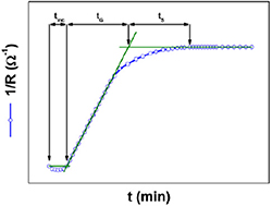
Figure 13. Typical time evolution of the electrical conductance 1/R of YBCO films during the isothermal growth stage. The identification of the different characteristics times is indicated: tinc is the incubation time, tG is the growth time and ts is the sintering time of YBCO grains. Reproduced from [156]. © IOP Publishing Ltd. All rights reserved.
Download figure:
Standard image High-resolution imagewhere R is the electrical resistance, G is the growth rate, tG the growth time and the rest are proportionality constants. Previous to this linear time dependence, an incubation time is also evidenced, which is related to the nucleation barrier to form stable YBCO islands and to the diffusion time required to reach percolation among them [156].
Through an analysis of the temperature dependence of G(T) for YBCO films it was possible to ascertain that the exponential dependence (van't Hoof equation) of the equilibrium constant Ke (Ke = Keo exp–(ΔHθ /RT), where ΔHθ is the reaction enthalpy) governing the reaction of equation (1) is the main parameter determining the observed strong temperature dependence of G (from 0.04 nm s−1 at 700 °C to 0.60 nm s−1 at 810 °C, i.e. a factor 15) (figure 14) and from this analysis the formation enthalpy ΔHθ of YBCO could be determined [156]. From this study it was also evidenced that the incubation time strongly depends on temperature, which reflects that because the in-plane growth rate is reduced it takes longer to achieve nuclei percolation. The typical nuclei separation distance was estimated to be ∼1 μm which is in agreement with previous estimated values [28, 164].
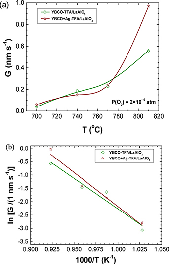
Figure 14. (a) Temperature dependence of the growth rate G measured for YBCO films grown from TFA and TFA-Ag solutions on an LAO substrate. (b) Analysis of the temperature dependence of the growth rate G measured for YBCO and YBCO-Ag films according to the law established from thermodynamic principles and chemical kinetics. The equilibrium constant of the reaction is assumed to follow the van't Hoof equation and so the standard enthalpies of the reaction, ΔHθ , can be deduced. Reproduced from [156]. © IOP Publishing Ltd. All rights reserved.
Download figure:
Standard image High-resolution imageAn additional complex problem associated to the BaF2 process that needs to be considered is the control of the supersaturation degree when thick films are being grown [28, 63, 139]. It was previously established that the gas controlled solid–solid reaction leading to YBCO should be analyzed differently in thin (up to ∼300 nm) and thick (beyond ∼600 nm) film limits [28, 139, 164]. While in the thin limit the classical nucleation energy barrier of a single nuclei is controlling the nucleation rate, in the thick limit the model needs to be extended to include the interaction among nuclei. As a consequence, the H2O gas flow and the diffusion permeability of the HF exhaust gas (equation (1)) across the films are also modifying the supersaturation degree and so the nucleation and growth rates [28, 139]. These two limits need to be taken into consideration when YBCO films with thicknesses in the range of ⩾1 μm are prepared.
While the general trends described up to now concerning nucleation and growth of YBCO films are valid with whatever REBCO film is considered, the precise optimal conditions for the different RE compositions and also in YBCO films with modified metal stoichiometry (Ba deficiency for instance) will be different because their corresponding equilibrium phase diagrams are slightly modified, i.e. the stability lines and optimal growth regions are shifted [57, 75, 169]. For instance, systematic analysis of different REBCO films grown under the same conditions showed a systematic shift of the superconducting properties (Tc, Jc ) [82, 83] while when larger RE ions are used (GdBCO for instance) the optimal growth conditions are shifted to lower PO2 values and higher temperatures [73], as compared to YBCO. We should note that (Y,Gd)BCO CCs with thicknesses in the range of ∼2.5 μm obtained through 15–20 depositions have been demonstrated with very high superconducting performance [63]. In the case of Ba deficient YBCO films, a decrease of the optimal growth temperatures was also demonstrated, very likely due to the shift of the stability line of YBCO in these Ba-poor compositions [74, 75]. The appealing consequence of this shift in the YBCO stability line is that the temperature dependence of supersaturation is also modified and so the crossover of the c-axis nucleation versus that of a/b grains is also shifted to lower temperatures. The main advantage of this shift is that high quality epitaxy (c-axis orientation) is achieved at lower temperatures with an improved microstructure (less porosity and a reduced concentration of a/b grains) [53, 74, 76, 80].
Understanding the main trends of REBCO nucleation and growth has strongly facilitated to prepare CCs using different metallic substrates (RABiT, IBAD) leading to fairly good superconducting performances, including the reel-to-reel continuous process used at industrial scale [30, 58, 140, 142, 169–172]. It is also worth to remark that owing to the global complexity of the CSD BaF2 growth process, several attempts of using experimental fast screening and big data approaches have been made to accelerate the optimization of CCs and to correlate processing, nanostructure and superconducting properties [143, 147, 173].
A special case of multilayer architecture requiring additional analysis of the growth conditions due to the relevance of the lattice misfit with the substrates or buffer layers is the case of YBCO films grown on sapphire. This architecture needs to handle the complex problem of the influence of strain in functional oxides. In the case of REBCO films grown through the BaF2 process it is even more complex because a partial relaxation of the interfacial strain occurs [174]. YBCO films grown on sapphire have appealing properties, both for MW and fault current limiter applications [175–177] and so extensive studies of the YBCO/CeO2/sapphire multilayer architecture have been performed in the past. In the case of MW applications, the required film thickness is quite limited (few hundred nm), while in the case of fault current limiters the film thickness should be as large as possible to reach high total critical current (Ic ) values [177]. Since early growth studies, however, it was found that, whatever film growth technique is used, the YBCO films displayed the formation of in-plane cracks when the film thickness goes beyond ∼250 nm, which was an evidence of the generation of an important tensile strain in the film. On the other hand, no equivalent tendency to generate cracks was detected when other substrates were used. The origin of this unique behavior of sapphire substrate remained obscure and it was generally associated to a strong difference in the thermal expansion of both phases (YBCO and sapphire). In a recent work, however, it was shown that the multilayer YBCO/CZO/YSZ/sapphire could be grown with thicknesses beyond 400 nm without crack formation and that, actually, the cracks appeared during the tetragonal–orthorhombic transition occurring during the oxygenation step [178]. A thorough analysis of the strain state of the different layers of this heterostructure showed that, while in the YBCO/CZO/YSZ multilayered structure the YBCO films keep a compressive state (no tendency to generate cracks) in the case of the sapphire substrate architecture the tetragonal YBCO films also keeps a compressive state but during the orthorhombic transition the decrease of the a-axis parameter is reduced versus the bulk value and so a tensile strain remains along this direction in the YBCO film and so a tendency to form cracks.
A final topic to handle is that related to the last step of the whole process of preparing REBCO superconducting films: the oxygenation process. It is well known that the oxygenation process of films is a complex problem which has been widely investigated mostly in the scope of the attractive properties of ionic and mixed ionic-electronic conductors [179–184]. However, the mechanisms responsible of the oxygenation process of YBCO films still remained poorly understood [185, 186]. In recent years, the particular case of YBCO CSD films has been extensively investigated by means of electrical resistivity relaxation measurements [158, 185, 186]. From the analysis of the temperature and PO2 dependences of the oxygen exchange kinetics for in-diffusion and out-diffusion processes it was concluded that the rate limiting step in thin films for the in-diffusion process is not the bulk diffusion of O2− ions. Instead, it was shown that the oxygen surface exchange is the slowest step and so it was shown that a catalytic effect accelerating the oxygenation kinetics (decrease of the activation energy) was achieved when Ag islands were included at the surface of the films. The study of oxygenation kinetics was later extended to other REBCO films and it was shown that a systematic shift in the activation energies and the optimal oxygenation temperatures exist for different REBCO films and also that the activation energies are modified by the oxygen chain ordering (O-I and O-II phases) of the oxygen deficient REBCO structure, thus suggesting that there is a crossover from the surface dominated domain to a bulk dominated domain [186]. Achieving a full understanding of the oxygenation kinetics in REBCO films is actually a very important issue because, as it has been recently demonstrated [187], the critical currents of the YBCO films in the OD state are strongly enhanced. Therefore, the determination of the rate limiting steps may allow to maximize the superconducting performance of films and CCs [188].
Summarizing, a steady progress in understanding the nucleation, growth and oxygenation stages of REBCO films preparation has been made in recent years which has been effectively used to improve the performance of CCs and technical substrates like sapphire. An important issue which still requires further progress is to develop procedures to increase the REBCO film growth rate in order to enhance the throughput in film manufacturing and so keep a strong competitiveness with other techniques where the growth rate is continuously increasing [8].
3.2. Nucleation and growth of REBCO with spontaneously segregated NPs
After the first reports of YBCO nanocomposite film growth by PLD [12, 189], the search of a suitable approach to grow nanocomposite YBCO films by CSD was immediately started. The first reports were based on an increase of the RE salt content in the starting solution (leading to Dy2O3 NPs in a YBCO films) [29, 30] while YBCO nanocomposites including BaZrO3 perovskite NPs were achieved in 2007 using complex solutions [22]. Extensive analyses of the nanostructure of these CSD films immediately confirmed that it completely differs from that generated by the techniques based on simultaneous growth of both phases (PLD or MOCVD) [22–24]. The main difference among both types of nanocomposites arises from the fact that the secondary NPs generated by CSD are mainly randomly oriented and randomly distributed. On the other hand, the growth techniques with a simultaneous growth of YBCO and the secondary NPs a self-assembled nanostructure of nanorods oriented perpendicular to the film substrate may be achieved [3, 14, 117, 121]. The driving force of the self-assembly phenomenon is the strain generated during the epitaxial orientation of both phases. This topic has been reviewed by several authors and it is not in the scope of the present manuscript [121–123]. Here we will focus our attention on the growth mechanisms of nanocomposites prepared by CSD using TFA or low fluorine precursors as an example of sequential method.
As we have previously described, the first SS strategy to prepare CSD nanocomposites was based on the use of complex metalorganic solutions including the elements required to form a specific secondary phase, for instance BaZrO3, BaCeO3, BaHfO3, RE2O3 or Ba2YTaO6 [22, 30, 89, 90, 190, 191] (figure 15(a)).

Figure 15. Schematics of the processes followed in chemical solution deposition to grow YBa2Cu3O7 nanocomposite films: (a) route based on the spontaneous segregation process where the metalorganic precursors include all the metal ions to be included in the final films; (b) route based on the preparation of preformed nanoparticles and a multifunctional colloidal solution including the metalorganic precursors and the stabilized nanoparticles.
Download figure:
Standard image High-resolution imageThe main question was to comprehend how the secondary phases nucleate and grow. In the SS approach to grow CSD nanocomposites the standard heating process (CTA) was applied and it was concluded that the NPs were embedded in the YBCO matrix with a high percentage randomly oriented (∼50%–90% depending on the concentration), except for the case of Y2O3 where the random fraction was smaller (<30%). From these results it was immediately suggested that the secondary phases (NPs) were created through homogeneous nucleation at lower temperatures than the epitaxial YBCO and so they were essentially randomly oriented [22, 23, 192]. Actually, a small percentage of the NPs was found to nucleate heterogeneously at the substrate interface and then they kept the epitaxy with YBCO (figure 16). In these cases, more complex textures were discerned by means of texture analysis with synchrotron x-ray diffraction. For instance, BaCeO3 NPs which have a large lattice misfit with YBCO display axiotaxy, i.e. a fiber axis preferential orientation versus the YBCO matrix [193].

Figure 16. XRD analysis to quantify the random and epitaxial fraction of nanodots in the nanocomposite films. (a) The 2D-XRD images centered at the (110) Bragg reflections of the BZO epitaxial nanodots allowing the quantification of the fraction of randomly oriented nanodots; (b) percentage of random nanodots versus nominal molar concentration Np in the YBCO nanocomposites with Y2O3, BaZrO3, BaCeO3 and Ba2YTaO6. Reproduced from [23], with permission from Springer Nature.
Download figure:
Standard image High-resolution imageAn important goal of the SS approach was the control of the NP size because their incoherent interface with YBCO is the source of induced defects in the YBCO matrix. The typical particle sizes achieved through the CTA growth process was in the range of ∼15–25 nm, depending on the composition and lattice misfit with YBCO, and it was concluded that there is a certain tendency to agglomerate the NPs at high concentrations [91]. The achieved particle size is very likely too large to have a direct effect on vortex pinning while the agglomeration effect decreases the specific interface with the YBCO matrix and so it decreases the positive influence on vortex pinning of the induced defects and it reduces the percolating critical current density Jc . The NP sizes were later studied and the influence of modified thermal treatments was undertaken by several authors to decrease the particle size and improve the distribution homogeneity [40, 80, 81, 91, 155, 194].
As we have mentioned above, BMO (M = Zr, Hf) or BYTO NPs nucleate mainly homogeneously at lower temperatures than YBCO (figure 17(a)) [40, 90]. The best strategy to decrease the particle size is, therefore, to enhance the nucleation rate in order to have a larger NP density and hence limit the particle growth. It is essential, therefore, to profit from the temperature dependence of the homogeneous nucleation rate which increases when temperature is reduced [37, 195, 196]. At the same time, it was necessary to know which parameters control the heterogeneous nucleation of BMO and BYTO at the substrate interface in order to avoid any disturbed interfacial nucleation of YBCO (figure 17(b)).
Figure 17. (a) 2D x-ray diffraction (integrated patterns) study of YBCO-10% BYTO/LAO films quenched from different temperatures; (b) TEM Z contrast image of a large epitaxially oriented BYTO nanoparticle on the substrate surface; (c) x-ray diffraction integrated θ–2θ scan of YBCO-10% BYTO samples at different stages of the growth process: pyrolysis, quenching at 575 °C for 10, 25, 85 and 180 min. The arrow identifies the 2θ position of the BYTO (220) reflection; (d) TEM Z contrast image of a YBCO-10% BYTO thin film after growth. Reproduced from [90]. © IOP Publishing Ltd. All rights reserved.
Download figure:
Standard image High-resolution imageIt was concluded that homogeneous nucleation of the NPs should be induced at lower temperatures, well below that of YBCO. As it is well known, the energy barrier for nucleation decreases with increasing undercooling (decreasing temperature) and so the NP nucleation density is enhanced at such lower temperatures [90, 195, 196]. The optimal heating profile should include, therefore, a two-step isothermal annealing, a first one to nucleate the NPs and a second one to nucleate YBCO. To ascertain at which temperature the first step should be performed and how long we need to wait, several quenched samples were examined, and it was found that, for instance, an intermediate annealing at 575 °C–580 °C during ∼60–85 min would be a good compromise to nucleate a high density of NPs while YBCO still has not been nucleated (figure 17(c)) [90, 92, 197]. There is no doubt that an improved homogeneity and a decreased particle size is achieved through this two-step process, as it has been confirmed by other authors with similar thermal annealing procedures [63, 198], even though these procedures still lead to results which are far from the desired tight control of the NPs size and distribution (figure 17(d)). A similar behavior concerning the NP size was also demonstrated in the case of GdBCO-Gd2O3 or GdBCO-BaZrO3 nanocomposite films, where the final particle size was in the range of 30–50 nm [70, 73]. In spite of the difficulties to keep small NP sizes, very competitive superconducting performances were already demonstrated in single crystal substrates, RABiT and IBAD CCs, including long length conductors [63, 73]. It was clear, therefore, that the films prepared through this procedure required an extensive analysis of their nanoscale defect structure and to correlate it with the observed enhanced superconducting performances. As we mentioned before, a very suggestive strategy was developed to keep a limited coarsening effect of the secondary NPs, i.e. the UTOC process based on taking profit of the CuO diffusion barrier formed at the interface of the multilayered pyrolyzed films [40, 80, 81, 92]. This process was successful to avoid the required atomic diffusion to promote NP coarsening and so the final NP size was kept rather small (∼13 nm) (figures 18(a)–(d)). The UTOC process leads to REBCO nanocomposite films with very high superconducting performances [40, 80, 81, 92].

Figure 18. (a) EDX elemental maps of the calcined films with donce (final film thickness of a single deposition) condition of 30 nm in an ultra-thin once-coating (UTOC) process; (b) and (c) schematic illustrations of the refining mechanism of BZO particles by the thinning of donce; (d) dependence on donce of the average size of the BZO particles in the YGdBCO + BZO CCs analyzed from TEM observations. Reproduced from [92]. © IOP Publishing Ltd. All rights reserved. Reproduced from [40]. © IOP Publishing Ltd. All rights reserved.
Download figure:
Standard image High-resolution imageIn conclusion, the SS strategy to grow REBCO nanocomposites has been successful as a tool to demonstrate that they can be prepared by CSD using the BaF2 approach and very competitive performances have been demonstrated, although several limitations of the methodology have also been stressed. For instance, it is still difficult to grow nanocomposite films with a tight control of the NP size and their distribution unless the UTOC process is used, which requires a very large number of deposition—pyrolysis cycles.
3.3. Growth of REBCO nanocomposites from multifunctional colloidal solutions
In the novel colloidal solution approach the NPs are previously prepared with a well-defined size and distribution, and stabilized as a colloidal solution with the corresponding RE, Ba and Cu metalorganic salts. Hence the approach should be suitable to achieve epitaxial REBCO nanocomposite films with a homogeneous structure at the nanoscale with small NPs, even at high concentrations. These nanocomposite materials should be a novel generation of thin films and CCs with enhanced performances at high magnetic fields.
The key actions to be undertaken and the requirements expected to be solved using this novel growth process are summarized in figure 19 [94].

Figure 19. Sketch of the different steps involved in the CSD colloidal solution approach to nanocomposite REBCO films. Reproduced from [94]. © IOP Publishing Ltd. All rights reserved.
Download figure:
Standard image High-resolution imageThe first difficulty detected was that the NPs could react with the elements to be included in the YBCO matrix and so form more complex oxide phases embedded in the YBCO matrix which disrupt the current percolation and also induce nucleation of undesired grain orientations of YBCO (ab-grains). This effect was first observed in YBCO nanocomposites including spinel NPs, such as MnFe2O4 and CoFe2O4 [114, 199]. Typical newly generated phases were YBaCu(Co)FeO5 double-perovskites, as identified by HAADF-STEM images, and the YBCO superconducting phase displayed reduced transition temperatures (Tc ∼ 40–76 K) and a coexistence of ferromagnetism and superconductivity at low temperatures, as reflected by SQUID magnetometry and XMCD spectra at the Cu L2,3 edge measured at 1.6 K and under high magnetic fields (6 T) [199].
More appealing results were achieved using the fluorite NPs CeO2, ZrO2 or HfO2 described in a section 2.2 [94, 96]. Several NP sizes and shapes were investigated to grow the nanocomposites and in all cases it was concluded that the NPs react with Ba forming BaMO3 (M = Ce, Zr, Hf) NPs. These studies also evidenced two additional difficulties which had to be overcome: the NPs may be pushed to the surface and the NPs may be accumulated at the substrate interface. The first phenomenon was widely described in several growth techniques [200–202] and it results from the fact that there is a pushing force of the YBCO growth interface to the NPs (proportional to the interfacial energy Δσo and the growth rate G) and a drag force opposing to it (proportional to a viscosity term η) which leads to a critical radius R* (∝Δσo/ηG). Depending on the particle size (r) and the growth rate of the film (G), the NPs are trapped if they are larger than R* (r > R*) or pushed if they are smaller (r < R*).
In the case of CeO2 NPs pushing was found to be certainly important because a high concentration of BaCeO3 (BCO) NPs were found in the film surface (displaying an important coarsening probably generated when they reach the film surface). In the case of ZrO2 NPs a tendency to nucleate as BZO at the substrate interface was detected. This tendency could be minimized by using a pristine YBCO layer as a seed layer, i.e. an ultrathin (∼50 nm) YBCO layer is first pyrolyzed. Additional multifunctional colloidal solution layers were then deposited on top of it and also pyrolyzed. The nucleation of YBCO at the interface occurs as a pristine film and the BZO NPs are fairly homogeneously distributed across the rest of the film (figure 20). Another route to minimize accumulation of NPs at the surface was shown to be associated to the pyrolysis process, i.e. when the heating ramp is increased the density of NPs at the substrate interface decreased and so the superconducting properties were improved [133]. In all these cases coarsening is in any case still quite relevant and the final NP size of the trapped BZO NPs lies in the range of ∼12–25 nm for an initial ZrO2 particle size of ∼7 nm [96]. It is clear, therefore, that the kinetics of the phase transformation from the fluorite to the perovskite structure is a key parameter to control the coarsening effects and so the final particle size. Certainly, a fine tuning of the initial particle size and the selected YBCO growth rate is required but the optimal values may also depend on the film thickness and the NP concentration. All in all, it has been shown that the two difficulties mentioned above, particle pushing and accumulation at the substrate interface, may be overcome by a fine tuning of the composition and processing conditions while the chemical reaction, although it enhances the complexity of the control of the film growth, may be fairly well controlled.
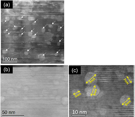
Figure 20. (a) STEM image of a 12% mol BZO low-fluorine YBCO-BZO film processed with a CTA process where the BZO nanoparticles are observed to be homogeneously distributed (white arrows); (b) and (c) STEM images of YBCO-20 mol% BHO (initial BHO size of 5 nm) YBCO nanocomposite processed following a flash heating process at 750 °C: (b) low-resolution image showing a general view of the YBCO nanocomposite layer and a seed layer; (c) high-resolution image of BHO nanoparticles showing that they display a minimal coarsening within the YBCO matrix. Reproduced from [91]. CC BY 4.0. Reproduced from [95]. © IOP Publishing Ltd. All rights reserved.
Download figure:
Standard image High-resolution imageA further step was made when stable and non-reactive BaMO3 (M = Zr, Hf) NPs became available [100, 103, 105]. These perovskite NPs do not disturb the REBCO composition (no chemical reaction) and they can be prepared in high concentrations and with tuned particle sizes keeping a narrow size distribution, therefore, they are ideally suited for a fine analysis of the relationship among growth, nanostructure and superconducting properties of CSD REBCO nanocomposites. The first report growing YBCO-BMO (M = Zr, Hf) nanocomposite thin films was made in 2018 [95], while further analyses were later reported with modified processing conditions to explore which are the optimal processing conditions. The initial particle sizes explored were in the range 5–10 nm with concentrations up to 25% mol. In the first attempts CTA was used as a heating profile and so some particle coarsening still existed during the heating process. As a result, the final NP size increased to values in the range of 10–20 nm. The distribution of the NPs, however, was more homogeneous and essentially they were randomly oriented, thus confirming that they were trapped during YBCO growth without any additional transformation.
In a more advanced YBCO nanocomposite growth approach, the same colloidal solutions were used but a FH thermal annealing process was used [91]. In that case the final NP sizes were very close to the initial ones (∼5–7 nm) and so it was concluded that coarsening effects were practically avoided. These nanocomposite films display the highest superconducting performances reported so far for films prepared by the multifunctional colloidal solution route to CSD nanocomposite films. Additionally, this approach was also valid for YSZ/SS ABAD metallic substrates and using multideposition methodologies to reach film thicknesses in the range of ∼700 nm [139].
In conclusion, we can assess that all the steps to be overcome to grow high quality nanocomposite films, as indicated in figure 20, have been achieved and so the epitaxial growth of nanocomposite REBCO films and CCs prepared from multifunctional colloidal solutions was successfully demonstrated.
4. Nanostructure and critical currents of REBCO nanocomposite films
4.1. Self-field critical currents: percolation currents
Achieving large total critical currents Ic (A cm−1-w) = Jc x d, where d is the film thickness (Ic being defined for a conductor of a 1 cm width), in CCs is one of the most relevant goals in the development of CCs, because most power applications and magnets require the highest engineering critical current density and the highest Ic values to minimize the conductor length and volume. This means that the self-field critical current Ic should be maximized, i.e. the film thickness d and the critical current density should be both as high as possible. We should remind at this point that the self-field Jc can be influenced by two different effects: the granular behavior of the conductors which decreases the percolating (or grain boundary Jc GB ) currents and the vortex pinning effects which enhance Jc in the single vortex pinning regime (or grain Jc G ) dominating at low magnetic fields (particularly the self-field region). The influence of grain boundaries on the transport critical currents in HTS has been widely reviewed before, as well as modeling of the percolating effect in CCs [203–207]. The main source of granularity is the underlying grain boundary structure of the metallic systems, however, the percolating models have been extended to the inhomogeneous systems (including pores or secondary impurities) which have also evidenced that a reduction of the self-field Jc may also occur in those cases [208–210].
In this section we will concentrate our attention into the recent progress in minimizing the annoying effects of the reduction of self-field percolating currents in REBCO films and CCs prepared through the CSD BaF2 process, while the influence of vortex pinning in the self-field current will be handled in a coming section. This topic was already previously reviewed and it was concluded that owing to the Volmer–Weber type of nucleation process some current blocking defects, including impurities or strain, may remain at the boundaries among different nucleated grains [20, 28, 69, 211, 212]. The main conclusion was that thermal annealing at high enough temperatures promotes a strong atomic diffusion which decreases the mesostrain accumulated at grain boundaries, and also that the nuclei distance should not be too long to avoid accumulation of impurities at the joining grains [69, 211, 213].
These issues were evidenced again in a recent study related to the growth of thick (∼1 μm) YBCO films on single crystal and ABAD metallic substrates [139] and it was also evidenced in a study of CCs based on RABiT substrates [36]. It turns out from these investigations that when a multideposition process is used there is a tendency to form a layered porous structure in the film after growth due to the layered CuO segregation at the surface of the pyrolyzed films which then, depending on the growth temperature may be improperly redistributed (figure 21). This is a typical source of self-field Jc decrease (figure 22) which is essentially avoided by proper selection of the deposition and growth processes [139, 192]. Another important source of negative influence on the self-field Jc values is the incomplete formation of the YBCO layer which then keeps some intermediate phases embedded in the YBCO matrix, for instance Y2Cu2O5, BaO, CuO or Y2O3 [53, 139, 192]. The formation of these secondary phases may be promoted by the interfacial reaction with buffer layers [161]. For instance, when CZO buffer layers are used there is a general trend to form BaCeO3 (BCO) at the interface which then consumes some Ba precursor and so the stoichiometry to form YBCO is not preserved. Another possible source of secondary phases may be associated to the use of non-stoichiometric starting solutions, as we have previously mentioned in section 2.1 [53, 149, 214]. The formation of these secondary phases has an immediate influence on the measured self-field critical current density because they reduce the surface cross section available for percolating currents. As it was mentioned in section 3.1, using a two-step growth approach and a YBCO seed layer including Ag which then allows to decrease the nucleation temperature, the self-field Jc at 77 K could be increased to high values (3.7 MA cm−2) thus leading to Ic values in the range of ∼400 A cm−1-w (figure 22). This successful processing methodology was also applied to ABAD CZO/YSZ/SS metallic substrates reaching Jc values in excess of 1 MA cm−2 and Ic values in the range of 120 A cm−1-w [139, 142].

Figure 21. (a) High-angle annular dark-field (HAADF)-STEM image of a thick (∼1 μm) film after quenching it prior to the nucleation temperature of YBCO; (b) low resolution STEM-HAADF image of a 1050 nm thick YBCO film grown on top of a CSDCZO/YSZ single crystal displaying some residual porosity; (c) and (d) STEM-HAADF images of secondary phases remaining after growth. The nature of each secondary phase is identified by EDX. Reproduced from [139]. © IOP Publishing Ltd. CC BY 3.0.
Download figure:
Standard image High-resolution image
Figure 22. (a) The evolution of Ic sf (77K) with YBCO film thickness using different deposition and growth techniques for single crystalline and metallic substrates. Dashed lines indicate the slopes corresponding to different critical current densities Jc sf at 77 K; (b) The temperature dependence of Ic sf (T) for different YBCO films having modified thicknesses and grown on different single crystalline substrates; (c) Jc sf (5 K) dependence with nanoparticle molar concentration (M) of YBCO-BZO (10 nm) preformed nanoparticles nanocomposite films (red triangle) compared with spontaneously segregated YBCO nanocomposite films (black sphere). Reproduced from [91]. CC BY 4.0. Reproduced from [139]. © IOP Publishing Ltd. CC BY 3.0.
Download figure:
Standard image High-resolution imageTo confirm that the reduction of self-field critical current may be indeed associated to a limitation in the percolating path, several studies were performed using an inductive experimental technique measuring minor hysteresis loops which identify the existence of return magnetic fields at the grain boundaries (Palau's method) and allowing the simultaneous determination of the percolating Jc GB and the intragrain Jc G [167, 203, 204]. When this technique was applied to a ABAD CZO/YSZ/SS conductor where the YBCO layers were deposited by IJP, it was concluded that the percolating current at 77 K Jc GB (1.8 MA cm− 2) was decreased by a factor ∼2 versus the intragrain value Jc G (3.3 MA cm−2), which was very similar to that measured in single crystalline substrates [142, 167]. An additional appealing information deployed by these inductive measurements is that the range of the grain size leading to a percolating current is ∼2.5 μm, i.e. a pretty small value which indicates that the nucleation rate of the YBCO grains was quite high and similar to that estimated by other routes such as the in-situ growth rate measurements described in section 3.1.
A similar conclusion concerning the nucleation density was achieved when the growth of YBCO thick films was performed in single crystalline substrates having different lattice mismatch with YBCO, such as LaAlO3 (LAO) and CZO/YSZ [139]. In the first case, there is a compressive mismatch  = (af
− ab
)/ab
, where af
is the lattice parameter of the film and ab
is the buffer layer matching distance, of = −1.56% while in the second case the misfit was = −0.52%. It is well known that strain is influencing the energy barrier for epitaxial nucleation and so the nucleation density [195, 215]. For that reason, it was concluded that in the CZO/YSZ substrate the nucleation density was higher than in LAO and so the percolating current density is enhanced due to a smaller grain size (figure 22).
= (af
− ab
)/ab
, where af
is the lattice parameter of the film and ab
is the buffer layer matching distance, of = −1.56% while in the second case the misfit was = −0.52%. It is well known that strain is influencing the energy barrier for epitaxial nucleation and so the nucleation density [195, 215]. For that reason, it was concluded that in the CZO/YSZ substrate the nucleation density was higher than in LAO and so the percolating current density is enhanced due to a smaller grain size (figure 22).
The analysis of the evolution of the self-field Jc with NP concentration in nanocomposites, either prepared by SS or from colloidal solutions, is also a good indicator about the quality of the corresponding films. For instance, if we compare YBCO-BZO nanocomposites prepared by SS with those from colloidal solutions (figure 22) we realize that a decrease of Jc occurs when the NP aggregation starts to be relevant and so the percolating current decreases. This happens in SS nanocomposites at around 7 mol% while with the preformed NPs in a FH process we can extend the NP molar concentration to ∼20 mol%. Of course, however, to be more precise it would be necessary to estimate in these films as well the extent of the enhanced vortex pinning contribution to increase the self-field Jc values.
The rules to develop large percolating critical current density in YBCO films grown through the BaF2 route have been now widely applied to several REBCO CCs using different substrates and the success in achieving high self-field critical currents has been widely demonstrated [28, 36, 207, 211]. We should mention, for instance, the extension of the CSD growth process to other REBCO compositions which required tuning the growth conditions (figure 23), and they were applied in Y1−x Gdx BCO conductors on RABiT and IBAD substrates [63, 169, 171, 216]. As it has been described previously (section 3.1), it was necessary to fine tune the temperature and PO2 conditions for growth to minimize the formation of BCO at the substrate interface and, depending on the quality of the buffer layer of the metallic substrate [58, 80, 81, 142, 171, 172]. Additional results confirming that the self-field critical currents are indeed decreased when the in-plane boundary angle among grain boundaries of the top buffer layer (cap layer) increases have been recently reported using IBAD substrates with CeO2 cap layers on top of the CC architecture. It was shown that Δφ values as low as 3° are required to keep the maximum Jc sf values [81].

Figure 23. Crystallization temperature dependence of the self-field critical current density Jc at 77 K for pristine and nanocomposite SmBCO-BHO films grown at an oxygen partial pressure of 50 ppm (black) or 150 ppm (blue). Reproduced from [217]. © The Author(s). Published by IOP Publishing Ltd. CC BY 4.0.
Download figure:
Standard image High-resolution imageIt is worth to note in any case that a significant effort to increase the self-field Ic values by increasing the REBCO film thickness has been made in different types of CC architectures using the BaF2 approach. Multideposition solution approaches and optimized growth procedures have shown that values at 77 K as high as Ic = 400–600 A cm−1-w can be achieved in films with thickness in excess of 2.5 μm and so we conclude that the CSD process based on BaF2 precursors are highly competitive in terms of performance [28, 31, 63, 212]. The main issue to achieve these high Ic values is to have a tight control of the defects limiting the percolating current, i.e. the secondary phases, the large pores and the a/b nucleated grains.
In conclusion, the general knowledge about the factors influencing the self-field critical currents in REBCO films and CCs is now well established and so there are well-defined rules to be followed to eliminate the reduction of superconducting performance associated to the percolating currents effect. Several types of metallic substrates, RE compositions in the REBCO films and deposition methods have been tested and it has been shown that through proper adjustment of the nucleation and growth conditions high quality epitaxial films can be obtained leading to very appealing superconducting performances, including the case of long length conductor production. It is concluded, therefore, that the CSD process using fluorinated precursors is a highly competitive approach in terms of low magnetic field superconducting performance.
4.2. Nanoscale defects generation: structure and properties
Research about the nanoscale defects and its corresponding functionalities in the complex structure of HTS is a top priority because the superconducting properties of HTS, particularly the critical current density Jc (T,B,θ), is strongly linked to the vortex pinning efficiency of these defects. Fortunately, new atomic scale analytical tools allowing to investigate the structure and to correlate it with the electronic and/or magnetic properties are now becoming available. We should particularly mention STEM-EELS which has become a unique methodology to systematically analyze the defect structure and strain effects of complex oxides. Epitaxial pristine and nanocomposite REBCO films grown on single crystalline substrates or the multilayered architectures of CCs are typical examples where these tools have become extremely useful [218–223]. Additional advanced characterization techniques with complementary insights, such as those available in synchrotron radiation facilities, for instance XMCD, have also helped to characterize the complex behavior of these materials.
In this section we will focus on the knowledge generated about the nanoscale defects in REBCO films and CCs grown through the BaF2 process, while in the next section we will describe how these defects influence the vortex pinning landscape of these materials.
Pristine YBCO thin films grown by the BaF2 process displays a complex microstructure which has been widely investigated in the past and several reports have been made [20, 36, 174] (figure 24). It was particularly noticeable that different types of dislocations exist, together with TBs, intergrowths or SFs, APBs and strained regions. Correlating the generation mechanisms of these defects with the film processing has been very challenging and it has attracted enormous interest from all the experts on thin film crystal growth as it was previously done in melt textured YBCO bulk ceramics [3, 20, 36, 91, 222, 224, 225].

Figure 24. Schematic representation of different defects present in YBCO films and nanocomposites. The pink regions represent the nanosized regions able to act as pinning centers. The dimensionality of the pinning centers (0D, 1D, 2D, or 3D) is also indicated. Reproduced from [226]. © IOP Publishing Ltd. CC BY 3.0.
Download figure:
Standard image High-resolution imageThe addition of secondary phases in YBCO thin films followed the activity previously done in melt textured grown bulk ceramics [227, 228] but with a much finer structure. The first epitaxial YBCO nanocomposites were reported in 2004 by using PLD and this discovery started a new era concerning the control of the defect structure in these materials [12, 189]. For CSD growth, since the first investigations of YBCO nanocomposites, it became clear that the nanoscale structure was very different from nanocomposite films grown by simultaneous deposition of both phases.
The most intriguing effect of the CSD nanocomposites was that the NPs were randomly oriented and so their interface with YBCO was not coherent, thus generating a high concentration of defects, such as SFs, dislocations and buckling of the YBCO structure [23]. The NPs of ∼10–20 nm displayed usually well-developed facets. The strongest impact of these NPs on the film nanostructure was the generation of a high density of SFs which extended along the whole film and they are surrounded by partial dislocations, as it is seen in cross section and plan view TEM images (figure 25). It was also shown, by using strain maps generated with STEM images, (figure 25) that the interfaces created edge dislocations while EELS mapping (oxygen K-edge pre-peak intensity) demonstrated that the interface functionality changes sharply, i.e. from the metallic to the insulating behavior. The SFs also created highly nanostrained regions, particularly at the partial dislocations surrounding these planar defects [23, 225, 229] (figures 26–28). Also, it was very relevant that short length SFs could be generated thus increasing the density of partial dislocations and so nanostrain (figure 28).

Figure 25. (a) HAADF-STEM image of an interface between YBCO matrix and a BHO nanoparticle. The inset shows a STEM simulation where a Ba–Cu–Cu–Ba (BCCB) lattice defect structure with an extra Cu plane corresponding to Y248 intergrowth; (b) measurement of the c-axis spacing variation in function of the distance; (c) low magnification plan view Z-contrast STEM image obtained along the [001] axis of a YBCO-BZO (13% mol) nanocomposite where two intergrowth's boundaries were identified and highlighted in yellow; (d) Z-contrast images of a YBCO-10% BYTO thin film where long SFs are visualized. Reproduced from [23], with permission from Springer Nature. Reproduced from [90]. © IOP Publishing Ltd. All rights reserved. Reproduced from [229]. © IOP Publishing Ltd. All rights reserved.
Download figure:
Standard image High-resolution image
Figure 26. (a) HAADF-STEM image of a BHO nanoparticle in the YBCO matrix. Note the sharp crystallographic facets with the crystallographic indices; (b) FFT of (a) with indexed diffraction data of the YBCO matrix (red) and the BHO nanoparticle (blue). The local variation and rotation of the g-vector (indicated in (b)) determined via local geometric phase analysis are shown in (c) and (d), respectively. Reproduced from [229]. © IOP Publishing Ltd. All rights reserved.
Download figure:
Standard image High-resolution image
Figure 27. Structural and superconducting properties as a function of vol.% of nanoparticle (BHO) additions and strain maps for pulsed laser deposition (PLD) and CSD (metal organic decomposition, MOD) nanocomposite films. (a)–(c) Normalized c-axis parameter, Tc
and Jc
s.f.
at 77 K as a function of vol.% of additions, respectively. (d), (e) High-resolution plan-view images, where xx, yy
and xy
maps were determined by geometrical phase analysis for BHO nanorod doped PLD-GdBCO and CSD-GdBCO +12 vol% BHO. The BHO nanoparticles were formed following the ultra-thin once-coating (UTOC) process with repetitive coatings (dcoat) of 30 nm. The horizontal bar scale indicates 5 nm for both (d), (e). Reproduced from [80]. CC BY 4.0.
Download figure:
Standard image High-resolution image
Figure 28. HAADF (a) and LAADF (b) images of an isolated 25 nm-long Y124 intergrowth. The yellow symbols in the images point to partial dislocations while the arrows to their surrounding strain fields. (c) HAADF image of a Y124 partial dislocation within the YBCO matrix. GPA yy
(d) and xx
(e) deformation maps along the <001> YBCO and <100> YBCO directions. The Bragg reflections taken for computing the images are the {100} and {003}, respectively. The marked region in the HAADF image is the reference lattice. (f) Enlarged image of the YBCO lattice near the BYTO showing the size and distribution of Y124 defects. Yellow symbols correspond to the partial dislocations associated to Y124. Reproduced from [225]. CC BY 4.0.
Download figure:
Standard image High-resolution imageA quantitative macroscopic determination of the existing nanostrain (%) in REBCO films can be made by means of x-ray diffraction using the Williamson–Hall plots [23]. In CSD REBCO nanocomposite films this parameter was found to be very strongly correlated to the density of partial dislocations surrounding SFs [23, 91].
Owing to the fact that a strong increase of the vortex pinning efficiency was detected associated to these defects (SFs and partial dislocations), it was concluded that nanostrain plays a key role in pinning vortices, as it will be discussed in the next section. However, it was also clear that the strain generated in the REBCO lattice of CSD films differs from that detected in systems where the secondary nanostructure has a coherent structure with REBCO (figure 27) [80].
Taking into account the key role played by SFs in the superconducting properties of the nanocomposites, it was worth to further investigate the structure and the functionality of these defects. The SFs were early identified by TEM as having the structure of the YBa2Cu4O8 (Y124) superconductor which differs from YBa2Cu3O7 (Y123) because there is a Cu–O double chain in the structure [230]. These defects had also been identified by TEM in melt textured ceramics, where they were closely associated to the Y2BaCuO5 particles [224, 231, 232]. In pristine YBCO thin films the concentration of these SFs was relatively low [174, 233] and so the influence on the overall stoichiometry was negligible. In nanocomposites, however, a very high density of SFs could be generated which immediately created a stoichiometry paradox, i.e. with an initial 1:2:3 Y:Ba:Cu ratio the final film was closer to a ratio 1:2:4 without any additional identifiable Cu provision. For that reason, a thorough atomic scale structural and functional investigation was undertaken, using STEM and XMCD in parallel with DFT calculations, which was then complemented by magnetometry measurements [218, 233, 234].
Accurate HAADF experimental images of the double chain structure of Y124 films from different origins were recorded and simulated and it was clearly concluded that, even if the crystal structure was that expected, the chains had a large concentration of atomic defect clusters (Cu and O ions) (figure 29) which after DFT calculations were identified as clusters including 2VCu + 3Vo, where VCu is a Cu vacancy and VO an oxygen vacancy (figure 29). The size of these clusters is in the range of 1 nm and the concentration along the chain is such that the overall metal stoichiometry is close to the original one of the film, i.e. 1:2:3, therefore solving the above mentioned stoichiometry paradox. There is no need actually of having a Cu excess to form such SFs, in agreement with experimental trials of thin film preparation with an increased Cu concentration that of thin film preparation with an increased Cu concentration (YBa2Cu4O8) which displays the same double chain structure without clusters of vacancies [218].
Figure 29. (a) Atomic resolution STEM image of the Y123 lattice with two Y124 intergrowths imaged along both the [010] and [100] orientation; (b) experimental STEM Z-contrast images of faulted Y124 viewed along the [010] zone axis; (c) formation energies and magnetism from DFT calculations for a Y124 structure with Cu vacancies at specific crystallographic position with its corresponding formation energy. (d) Isosurface plot showing the spin density associated with a 2 VCu + 3 VO defect in Y248 along with an integrated magnetization/area profile along the z-axis. Reproduced from [218]. CC BY 4.0.
Download figure:
Standard image High-resolution imageStill a further step is to know what is the functional behavior of these defective SFs. As it is well known, stoichiometric Y124 phase displays superconductivity with a decreased Tc (Tc ∼ 75–80 K) [235], however, what is the influence of the atomic vacancy clusters?. Actually, DFT calculations predicted that the Cu ions neighbors of the cluster should display a ferromagnetic order similar to that of diluted ferromagnetic semiconductors, and so a highly sensitivity and atomic-selective technique should be used, such as XMCD at the Cu edge under applied magnetic fields. By measuring the difference in x-ray absorption between left- and right- handed polarizations, it is possible to determine unambiguously the atomic magnetic moments, even with low concentrations. From the magnetic field and temperature dependencies of the measured magnetic moments it was concluded that several Cu ions couple ferromagnetically and that these magnetic clusters behave superparamagnetically with a magnetic moment in the range of 1.18 μB [218, 233]. Such unexpected ferromagnetic defects should have a strong influence on the superconducting behavior of the REBCO nanocomposite films as will be further discussed in the next section. To further characterize the superconducting character of these defective SFs, a study of the superconducting properties of CSD grown pristine ultrathin (10–50 nm) YBCO films was undertaken. The interest of such films is that they display a very high concentration of SFs, probably due to the influence of strain associated to the substrate. A quantitative relationship among superconducting volume determined from the shielding percentage and SFs concentration, determined from x-ray diffraction patterns, was determined. The most striking conclusion was that the defective SFs should behave as non-superconducting not only at the substrate interfaces but, very likely in the bulk of YBCO films. Very likely Cooper pair suppression occurs at the defective Y124 structure in parallel to the ferromagnetic order mentioned before. As a consequence, one should expect that the SFs play an important role as APC, as we will discuss in the next section. In any case, it is clear that a very important analysis of the microstructure of nanocomposite films is related to the quantification of the length and concentration of these planar (essentially circular) defects laying parallel to ab planes.
This analysis was performed in several CSD nanocomposites (CTA and FH annealing) and it was compared to pristine films, and the results are displayed in figure 30. It is clear that a high concentration of very short SFs (less than 10 nm) is achieved in FH YBCO-BHO nanocomposites prepared with preformed NPs. As we will see, these are among the champion films in terms of vortex pinning efficiency thus confirming the key role of these defects. It is also worth to mentioning that the concentration of these SFs in YBCO CCs can be enhanced by performing post-annealing treatments under O2 atmosphere or oxygenating under different conditions [236, 237], thus corroborating that the stoichiometry paradox mentioned before is solved through the formation of Cu vacancies, and confirming the positive role of these defects to enhance the critical currents if there are short enough to strongly increase the concentration of the partial dislocations surrounding them.
Figure 30. STEM images of YBCO-20 mol% BHO nanocomposite with preformed nanoparticles (5 nm) processed following with flash heating at 750 °C. (a) High-resolution image of an isolated BHO surrounded by short intergrowths (indicated by yellow arrows); (b) histogram showing the length and number of intergrowths for FH and CTA process in YBCO pristine and YBCO-BHO nanocomposite films with preformed nanoparticles. Reproduced from [91]. CC BY 4.0.
Download figure:
Standard image High-resolution imageBesides the direct role played by SFs in the functionality of YBCO films, it has also been shown that they have an indirect role on other defects of YBCO films. We should particularly refer to TBs which, as it is well known, play a key role in many vortex dynamic phenomena (channeling, creep, etc) [238]. By using STEM images recorded by HADDF and LAADF and performing GPA strain mapping, it was possible to determine the orientation of different twin domains ([100] and [010]) and to localize the TBs [225, 226, 239]. It was immediately clear that the intergrowths strongly interact with TBs forcing them to lose the coherence along the c-axis and thus shortening the length of these planes perpendicularly to the film substrate (figure 31).

Figure 31. (a) A composition of consecutive atomic resolution Z-contrast images along a particular Y124 planar defect of a YBCO nanocomposite cross-sectional specimen; (b) xx
deformation map showing in colors (red and green) different deformation values. Region 3 in (a) was taken as a reference area; (c) Close up views of regions 1 and 2 labeled in (a) corresponding to two sides of a twin boundary, which permits determination of the [010] and [100] zone axes in (b). The brightest spots correspond to Ba columns, followed by Y and finally by Cu, being the darkest contrast shown by the atomic planes containing Cu–O chains; (d) twin boundary domains in a highly distorted region of a 10% BYTO YBCO SS-nanocomposite. Green and brown colored regions mark different twin domains, corresponding to [100] and [010] YBCO zone axes, respectively. Dashed-vertical lines mark the limit of the twin domains. The inset shows a close-up view of a TB. Reproduced from [226]. © IOP Publishing Ltd. CC BY 3.0. Reprinted from [239], with the permission of AIP Publishing.
Download figure:
Standard image High-resolution imageAdditionally, TBs are also strongly disturbed by the strain fields associated to the embedded NPs [239]. It is clear, therefore, that any analysis of the influence of TBs on the superconducting properties should take into account the strong interaction of them with the existing SFs and so both defects will need to be quantified to reach conclusive evidences about their respective roles on the properties. These analyses clearly show that it is very important to understand under which growth or post-annealing conditions the SFs in REBCO films are formed. For instance, it has been suggested by some authors that (Y0.77Gd0.33)Ba1.5Cu3O7 films, when grown at significantly low temperatures (≈740 °C), create a low concentration of SFs and so TBs keep a high coherence along the c-axis [240–242].
An even more detailed study of the atomic structure of the YBCO defects, particularly the SFs, was carried out correlating accurate local probe STEM-EELS imaging with DFT calculations [223, 243]. These works concentrated in the elusive behavior of oxygen ions in the YBCO structure which, as it is well known, have a strong influence on the electronic structure and superconducting properties [244, 245]. The key point has been for years, to know where the oxygen vacancies are located within the YBCO structure. It has always been assumed that only the Cu–O chains accept VO, however, recent works have actually shown that at low oxygen vacancy concentrations other crystallographic positions could also accept VO. Specifically, comparing atomic resolution STEM images in the vicinity of Y124 intergrowths with pristine films, complemented with EELS analysis and DFT calculations, it was concluded that some VO also exist in the apical position joining CuO2 pyramids with the Cu–O chains and this occupancy distorts accordingly the buckled structure of the CuO2 planes [243]. The actual occupancy of these positions was confirmed to be promoted by local strain which drives the oxygen migration [223]. The most relevant consequence of this unexpected position of the vacancies is that the charge transfer to the planes is modified, as confirmed by Cu L and O K edge EELS spectra, which differ if they are close to these vacancies or not, and also by band calculations which show a shift in the density of states in positions close to the apical vacancies [243]. Overall, therefore, it is clear that further progress is required to reach a tight correlation among defect structure and functionality in the complex structure of YBCO. For instance, it is actually unknown at which point the described defect structure is modified when other RE ions are used in this structure. As we have already described before, the influence of RE ions on the local crystal structure, thermodynamic and superconducting properties is not negligible at all and so the atomic defect structure should be also further investigated to reach firm conclusions concerning their influence on the superconducting properties.
4.3. Vortex pinning landscape: relationship with NPs and induced defects
Advances in understanding vortex pinning in type II superconductors has been one of the biggest challenges in the area of these materials and, after the discovery of HTS the topic regained the highest priority because the performance of these materials in practical applications is fully linked to the efficiency of defects to pin vortices at high magnetic fields and high temperatures. The establishment of a direct correlation between atomic and nanoscale defects, which could act as APCs, and their impact on the superconducting properties has been a captivating research area. Since the discovery of HTS this topic has generated an extensive body of literature, comprising thousands of articles. However, due to the scope of the present review, it is not feasible to discuss all of them here, and we refer interested readers to the numerous existing reviews on this subject [3, 24, 220, 246–251].
The main difficulty in the analysis of the vortex pinning landscape in HTS is to find a practical methodology allowing to identify the influence of specific defects of different dimensionality and orientation on the observed temperature, orientation and magnetic field dependence of the critical current density Jc (T,θ,H). A very useful approach to correlate the defect landscape with vortex pinning properties was developed which assumes no interaction (or weak interaction) between different pinning centers and thus their contributions may be simply summed up [22, 23, 226, 252]. Other authors have also modeled the experimental Jc (T,θ,H) values through statistical procedures not directly linked to specific microstructural features [253].
Three basic vortex pinning contributions were considered to influence the overall landscape: anisotropic-strong, isotropic strong and isotropic weak [22, 194, 252, 254]. The temperature and magnetic field dependences of these different terms were clearly identified and so H–T magnetic phase diagrams were defined indicating the relative strength of the three contributions and how they are influenced by the intrinsic defect structure or the concentration of APCs, such as NPs or nanorods.
Concerning the isothermal magnetic field dependences Jc (H,T) they are usually defined on the basis of three different regions and the analysis can be applied to either H//c or H//ab. The low magnetic field region I in figure 32 corresponds to the situation where Jc (H) is constant because vortices interact weakly with each other but strongly with defects, i.e. we are in the single vortex pinning region. The shift towards the regimes where vortex–vortex interaction is already at least as large as the core pinning of a single vortex is marked by H*(T), where H* is the crossover magnetic field towards region II. This magnetic field sets the limit between the single vortex pinning regime and the collective pinning regime where vortex–vortex interaction is very relevant. Therefore, H* is related to the density of defects and it can be used as an indicator of the concentration and pinning efficiency of the APC and pre-existing defects. It has been customary to define it by the equation Jc (H*) = 0.9Jc sf , where sf stands for self-field. Region II in figure 32 is usually defined by a power law dependence, Jc ∝ H−α , where the α parameter depends on the defect density and pinning strength. Actually, time-dependent Ginzburg–Landau simulations confirmed this power law dependence and showed a decrease of α values, simultaneously to the increase of Jc (H), when the NP concentration was increased [247, 248, 255]. Finally, region III is characterized by approaching the irreversibility field and then Jc (H) has a much faster decay and also thermal activation effects are reflected in an enhanced flux creep coefficient (figure 32) [256–258].
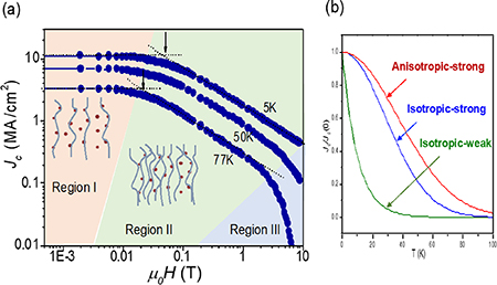
Figure 32. (a) Typical magnetic field dependence of Jc (H) for REBCO films at different temperatures with the three main regions that determine the Jc (H) behavior indicated; (b) Temperature dependence of different pinning center contributions considering their characteristic average vortex pinning energies. All the measurements were performed with H//c. Reproduced from [226]. © IOP Publishing Ltd. CC BY 3.0.
Download figure:
Standard image High-resolution imageThe temperature dependences of the three contributions to Jc (T) reflect the effectiveness of vortex pinning energy versus thermal activation. They can be described following existing vortex pinning models for weak collective pinning predicting an exponential dependence with T and the Bose glass theory to describe strong correlated pinning centers where it is predicted that Jc decays as an exponential function of T2 [226, 259]. This modeling approach was previously used successfully as well to the analysis of melt textured YBa2Cu3O7-Y2BaCuO5 bulk ceramics with modified microstructural effects, including SFs, TBs and secondary phases [224, 231, 260–262]. In REBCO thin films it has been shown that anisotropic defects act only as strong pinning centers, whereas isotropic defects can be point or nanosized defects, promoting either a weak or a strong pinning behavior. Therefore, the total Jc (T) can be described by the linear sum of three contributions [194, 226, 246, 252, 259]:
where Jc iso-str and Jc aniso-str are the isotropic-strong (iso-str) and anisotropic-strong contributions and the isotropic-weak (iso-wk) contribution is Jc iso-wk. Owing to the fact that vortices are mainly pinned based on the core pinning mechanism, in this equation the zero temperature values Jc (0) are the Jc values in absence of creep, thus they are related to the density and strength of the corresponding pinning centers. On the other hand, the characteristic pinning energies of the different defects are reflected in the different ranges of fitting temperatures To and T*, which indicate the stability against thermal excitations [194, 226, 252].
As it has been widely reported in previous analyses of the vortex pinning landscape in REBCO films and CCs derived from fluorinated solutions [20, 23, 24, 226] and as we have described in section 4.2, in REBCO films there exists a wide range of intrinsic defects which can be described accordingly to their dimensionality (0D, 1D, 2D, 3D), orientation and strength. Their efficiency as APC depends on the dimension of the perturbed region where the superconducting order parameter is strongly depressed (which ideally should be in the range of the coherence length ξ). On the other hand, in nanocomposite thin films an additional contribution should be generated associated to the secondary nanophases (NPs, nanorods). In this case, the size of the nanophases Dnp should be in the range Dnp ⩾ 2ξ to become strong pinning centers.
A thorough investigation of the critical current density measured in an extended range of pristine and nanocomposite YBCO thin films prepared by CSD (>30 samples) with thicknesses in the range 150–850 nm, including different types of NPs (BZO, BHO, BYTO, Y2O3), concentration and processing methodologies (SS and colloidal solutions), has been recently reported [91, 194, 263]. The analyses include Jc (H) measurements up to ultra-high magnetic fields (35 T) and with the H//c and H//ab magnetic field orientations (figure 33). This work outlined that a very systematic behavior exists to correlate defect concentrations and pinning efficiencies which we will here summarize.
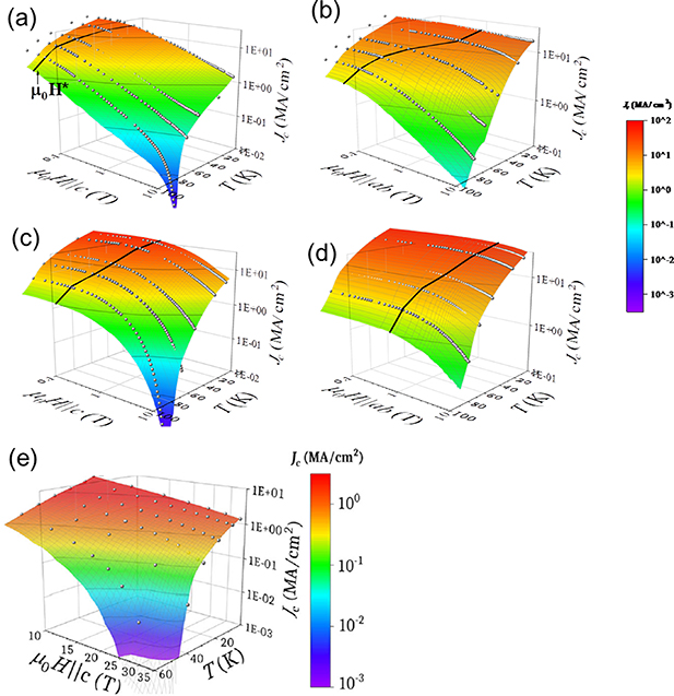
Figure 33. Jc (H,T) measurements at magnetic fields up to 9 T for (a), (b) a pristine and (c), (d) a nanocomposite (10%BZO + 5%YO) for (a), (c) H//c and (b), (d) H//ab; (e) Jc (H,T) measurements at magnetic fields up to 35 T for a thin (150 nm) nanocomposite (BHO) film. Spherical symbols represent the measured Jc (H) curves and solid lines correspond to the accommodation magnetic field μ0 H*(T) curve. Reproduced from [194]. CC BY 4.0.
Download figure:
Standard image High-resolution imageFrom the whole set of Jc (H,T) measurements performed with H//c and H//ab in several samples (pristine and nanocomposites) the first parameter which may be shown to evolve is the crossover magnetic field H* which is clearly enhanced in nanocomposites, as compared to pristine YBCO films, for both magnetic field orientations (figure 34). The origin of this enhancement has been widely investigated in order to clarify which defects are the main responsible of vortex pinning in this single vortex pinning regime.

Figure 34. Exponential H*() trend. For (black) pristine, (red) spontaneous segregation nanocomposites and (blue) preformed nanoparticles nanocomposites: μ0
H* at (a), (b) 77 K, (c), (d) 50 K and (e), (f) 5 K for (a), (c), (e) H*//c and (b), (d), (f) H*//ab versus nanostrain. Dashed lines are guides to the eye; (g) dependence of the normalized maximum isotropic pinning force Fp
max iso/Fp
tot max of all a nanocomposite series on the nanostrain determined from the Williamson–Hall plots; (h) dependence of the μ0
H* at 5 K on the nanostrain for pristine YBCO and YBCO-BMO preformed nanoparticles nanocomposites comparing composition (BHO vs. BZO) and size (5 nm vs. 10 nm) of the nanoparticles in CTA (25 °C min−1) and for the FH (1200 °C min−1) at different thickness (150 nm, 250 nm and 350 nm); (i) sketch of vortex pinning of both small nanoparticles (NPs) and partial dislocations. Reproduced from [91]. CC BY 4.0. Reproduced from [194]. CC BY 4.0. Reproduced with permission from [264].
Download figure:
Standard image High-resolution imageAs it has been already mentioned in the previous section, a characteristic feature of YBCO nanocomposites is that the secondary phase BMO (M = Hf, Zr) NPs generate a high concentration of SFs and these defects are surrounded by partial dislocations where strain is very strong. As a consequence, the film nanostrain (%) determined through x-ray diffraction (Williamson–Hall measurements) is a powerful route to quantify the strain generated by dislocations and to correlate it with the single vortex pinning efficiency [23, 91, 105, 194]. Figure 34 shows first that a direct correlation exists between H* and for H//c in samples having different concentrations and lengths of SFs, as previously shown in figure 30. Actually, the volume of partial dislocations could be properly quantified by using STEM images allowing to determine the lengths of the SFs, and hence the concentration of partial dislocations [91, 194]. For instance, it was clarified that the SFs are shorter and more abundant when YBCO films are processed through a FH process because the BHO NPs remain smaller than in a CTA process. The strong correlation between H* and was later on confirmed by extending the analysis to many more samples and also to the H//ab orientation and other authors also confirmed this trend (figure 34) [105, 194]. It is worth to signal that this correlation is effective in all ranges of temperatures and orientations thus confirming that the nanostrain originating it has an isotropic behavior and behaves as a strong APC.
The effectiveness of as a measure to quantify the pinning strength was also demonstrated by looking at the evolution of the maximum pinning force Fp
max iso associated to isotropic Jc
isostr (figure 34) and to the Jc
values at a specific magnetic field (1 T) and the α parameter determining the magnetic field dependence in the collective pinning region (figures 32 and 35) [105]. It was concluded, therefore, that the created strained regions behave as isotropic APCs, a conclusion also reached by other works where nanostrain was created through artificial structuration with (Ba,Sr)TiO3 micropillars embedded in the YBCO lattice [265]. We should wonder, therefore, why the nanostrained regions in the HTS lattice become non superconducting and thus behave as APC. This is an unprecedented phenomenon in superconductivity which has been explained by a new microscopic mechanism: the bond-contraction pairing model [266–268]. The model stresses the critical role of interatomic Cu–O distances (dCuO) in pair formation because the transfer integral has a strong power dependence with dCuO (tCuO ∝  ), where tCuO is the transfer integral between 3d orbitals of Cu and 2p orbitals of O in the CuO2 square lattice of YBCO, therefore, a small tensile strain may quench the pair formation and hence create non superconducting regions at the nanoscale [23, 265].

Figure 35. Correlation among the pinning properties at 77 K in YBCO-BMO nanocomposite films including BHO, BZO and SZO nanoparticles. (A) Accommodation field (H*); (B) power–law exponent α; and (C) normalized Jc
at 1 T and the nanostrain (00l). H* and the normalized Jc/Jco
value at 1 T show a nearly linear correlation with 00l, while α shows a polynomial decrease with 00l. Reprinted with permission from [105]. Copyright (2020) American Chemical Society.
Download figure:
Standard image High-resolution imageIt is also worth to note, however, that not only nanostrain influences H*, as it is clearly evidenced in figure 34(h), where the nanocomposites having the smallest BHO NPs show enhanced H* values while having the same value. The interpretation of these results is that, in addition to the vortex pinning contribution arising from the partial dislocations these samples have also a direct contribution of the NPs by themselves, i.e. the small size (initially 5 nm) fulfills the requirement for core pinning being effective [269]. A direct demonstration of the effectiveness of small (≈7 nm) BHO NPs in pinning vortices in the single vortex pinning regime was also reported through direct Jc
sf
measurements in YBCO-BHO nanocomposites [91] and in (Y,Gd)BCO-BHO nanocomposite films (figures 35 and 36). The YBCO and (Y,Gd)BCO nanocomposite films clearly showed enhanced Jc
sf
values at all temperatures when fine NPs were added [80, 81, 91]. We should note here that a very high NP density has been reached in these two studies using NPs sizes around 5–7 nm (nnp
∼ 1022–1023 np m−3) which corresponds to a volume percentage of the secondary phase of ∼8% vol [80, 91], i.e. a very similar value to that achieved in the best PLD or MOCVD nanocomposites [270, 271]. It was also clear that for a given volume of NPs the density of them increases when the size is reduced and so Jc
sf
is further enhanced, as expected from a strong pinning analysis of the influence of NPs in the single vortex regime (figure 36) [80, 81]:


Figure 36. Nanoparticle density nnp and self-field Jc sf as a function of vol % of nanoparticle addition for (Y,Gd)BCO + BMO films. (a) BaMO3 (BMO, M = Hf, Zr, Sn, Nb) nanoparticle density as a function of volume percent of addition for (Y,Gd)BCO + BMO films obtained from several TEM images. Open and solid symbols represent data of films with different nanoparticle sizes obtained by UTOC using dcoat = 150 and 30 nm, respectively. (b) Jc sf at 77 K as a function of volume percent of addition for (Y,Gd)BCO + BMO films. Inset: Jc s.f. at 77 K versus nanoparticle density for films with 12 vol.% of different dopants. Reproduced from [80]. CC BY 4.0.
Download figure:
Standard image High-resolution imagewhere Nnp is the density of the NPs, D is the mean size of the NPs, ξab is the coherence length, λab is the London penetration depth, and Hc is the thermodynamic critical field.
To gain more insight on the nature of the vortex pinning mechanism in this single vortex pinning regime, it is worth examining which is the dominating nature of the defects. This can be accomplished by looking at the magnetic phase diagrams showing the Jc iso/Jc and Jc aniso/Jc ratios, as determined by fitting with equation (5). Figure 37 displays typical results for H//c and H//ab and includes also the corresponding H*(T) lines. As it may be observed, all the H*(T) lines are immersed in the regions where the isotropic contribution to Jc is dominating, thus supporting the idea that both the partial dislocations and the NPs contribute to enhance H*, moreover this is true for both field orientations thus suggesting that the same sort of defects are effective. Actually, more detailed analyses of Jc (T) [226] have shown that at low temperatures (T ≈ 5 K) the isotropic contribution arises from both strong and weak contributions. While the origin of the strong pinning contribution seems to be directly associated to the partial dislocations of the SFs and to the NPs themselves, the weak pinning contributions have been ascribed to point defects. In the present case, in addition to possible oxygen vacancies we know that we have a huge concentration of complex point-like defects in the chains of the SFs where, as we have described in the previous section, we have ferromagnetic clusters of Cu vacancies decorated by O vacancies. These defects will certainly behave as point-like vortex pinning centers and so the increase of the isotropic strong pinning contribution encompasses an increase of the isotropic weak pinning contribution.
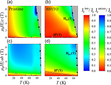
Figure 37. μ0 H–T color map of the ratios Jc iso/Jc and Jc aniso/Jc for (a), (c) a pristine and (b), (d) a nanocomposite for (a), (b) H//c and (c), (d) H//ab. Solid lines with circles and triangles mark the μ0 Hirr(T) and μ0 H*(T) curves, respectively. Reproduced from [194]. CC BY 4.0.
Download figure:
Standard image High-resolution imageGoing further in the analysis of the vortex pinning landscape requires to investigate the high magnetic field regimes where vortex–vortex interaction plays a key role and so collective effects determine the Jc (H) dependences. Following the same schematic analysis devised before (equation (5)), the magnetic field dependence of all the fitting parameters were determined after fitting the corresponding temperature dependences, as it can be appreciated for typical samples in figure 38. The first feature to note is that the characteristic temperatures measuring the relevance of thermal activation effects (To, T*) clearly follow the expected trend. Thermal activation effects are the highest for isotropic-weak contributions, the lowest for anisotropic-strong contributions and intermediate for isotropic-strong contributions.

Figure 38. Magnetic field dependence of characteristic temperatures: (a) T0 (solid lines), T*iso-str (solid lines) and T*aniso-str (dashed lines), and Jc contributions at 0 K (b) Jc aniso-str, (c) Jc iso-str and (d) Jc iso-wk for pristine (pr) films and for nanocomposite films grown from colloidal solutions (pn). All the parameters were obtained by fitting with equation (5). Reproduced from [194]. CC BY 4.0.
Download figure:
Standard image High-resolution imageThe small modifications of these temperature ranges among different samples are indicative of the same type of defects contributing in different samples with small rearrangements of the defect structure among them [194]. On the other hand, the magnetic field dependence of the fitted values of Jc
(0) and To
or T* (figure 38) clearly shows a different evolution signaling how the vortices adapt to the existing defects, as well as how efficient they are when the magnetic field is increased. For instance, it is clearly ascertained that the strong pinning defects decrease its efficiency at high magnetic fields (decrease of T*(H)) while the efficiency of the isotropic-weak pinning defects is maintained or slightly enhanced (increase To
(H)). In all cases the efficiency of the existing vortex pinning centers, as measured by the Jc
(0) values, decreases although at different paces for strong and weak pinning centers. For that reason, in ultrahigh magnetic fields (H > 30 T) in some cases the pristine YBCO films may even display higher Jc
(H) values. This is an issue whose origin deserves further analysis. An additional evidence of the efficiency of nanostrain in enhancing vortex pinning in the collective regime was recently provided when the power law parameter α was found to scale with nanostrain , similarly to H* in the single vortex regime, in YBCO-(Ba,Sr)MO3 nanocomposites (M = Zr, Hf, Ti) (figure 35) [105]. In this temperature range it has also been shown that proton irradiation generates defects having a size of a few nm which are effective APCs [272].
Concerning the maximum pinning force densities Fp max measured in CSD nanocomposites when H//c, we should note that very significant increases have been demonstrated in different optimally doped REBCO (RE = Y, Gd, Sm) films and CCs, achieving excellent pinning performances at different temperatures, very close to those displayed by CCs at H//c grown through in-situ approaches (PLD, MOCVD) having nanorod APCs [3, 73, 216, 217, 221, 273–278].
An additional advantage of nanocomposite REBCO films and CCs grown by CSD, as compared to those displaying a nanostructure including nanorods parallel to the c-axis, is that the Jc
(H,θ) curve increases in the whole angular range. The analysis of the anisotropy of physical properties in one band superconductors can be described using the electronic mass anisotropy given by the ratio γ = (mc
/mab
)1/2, where mab
and mc
are the effective masses along the ab and c directions. In that case the physical parameters can be scaled (Blatter scaling approach) using the parameter (θ) = [cos2
θ + γ−2sin2
θ]1/2 [246]. This applies, for instance, to Hc
2(T), Hirr(T) and Jc
(H,T) [254, 279].
The intrinsic anisotropy γ applies to the thermodynamic parameters, while an effective pinning anisotropy γeff, determined from extrinsic magnitudes like Jc (H,T,θ) or Hirr(T,θ), which depend on vortex pinning, is required. This controversy in REBCO films has attracted the interest of several studies which examined the liquid and solid vortex regimes through different experimental techniques [23, 254, 279–281]. For instance, angular resistivity measurements, i.e. the long-range vortex displacement regime, performed at different temperatures under ultra-high magnetic fields (<65 T) allowed determining the intrinsic mass anisotropy γ from the measured Hc 2(θ) values. On the other hand, complex resistivity measurements at MW frequencies allowed determining the anisotropy of the flux flow resistivity [263, 281, 282], i.e. in the low vortex displacement regime, in nanocomposite YBCO films with different degrees of NP concentrations. In both cases it was found that the intrinsic mass anisotropy remained constant γ ≈ 5–7, independently of the pinning strength, thus demonstrating that the intrinsic superconducting properties were not modified by the secondary NPs [23, 280].
On the other hand, the effective pinning anisotropy γeff has been determined from the Blatter scaling approach for anisotropic superconductors applied either to the isotropic contribution to Jc
(H,θ) (figure 39) or to the irreversibility line Hirr(T,θ). The scaling takes into account in this case that near H//c and H//ab there exists additional anisotropic pinning contributions arising from the TBs, in the first case, and the SFs or the intrinsic pinning for the second case (figure 37) [23, 242, 256, 280]. In both types of measurements, it was shown that γeff decreases with the thin films nanostrain , as measured from x-ray diffraction patterns, from γeff ≈ 5–7 to γeff ≈ 2.5 (see figure 40). This result confirms that the partial dislocations surrounding the SFs, which are the main contributors to , have a dominant influence in strengthening the isotropic strong pinning in the REBCO nanocomposites.
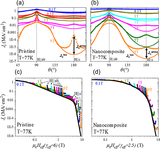
Figure 39. Jc (θ) as a function of μ0 Heff with corresponding γeff for (a) pristine and (b) YBCO 6% mol BYTO-5% mol BZO films at 77 K. The dashed line is the identification of the collapsed Jc iso(Heff) line. Deviations from the collapsed values are identified for orientations close to H//ab and H//c for the pristine film; Jc (θ) dependence at 77 K for (c) YBCO pristine film and (d) YBCO 6% mol BYTO-5% mol BZO thin films. The solid lines correspond to the isotropic contribution Jc iso(θ) obtained from the collapse achieved in (a) and (b). Double-headed arrows indicate Jc aniso(9 T, H//c, 77 K). Reproduced with permission from [264].
Download figure:
Standard image High-resolution image
Figure 40.
μ0
Hc
2 as a function of the reduced temperature T/Tc
for different magnetic-field orientations in a YBCO-15% mol BYTO nanocomposite film. Measurements performed from isothermal magnetoresistance measurements under pulsed magnetic fields up to 65 T. Inset: collapse of three curves using a γHc2,res = 5.4 ± 0.3. (b) Dependence of effective anisotropy factor (γeff) and the intrinsic anisotropy factors, determined from resistive measurements in high fields (γHc2,HF), resistive measurements (γHc2,res) and microwave measurements (γMW), as a function of the nanostrain (%) for a series of studied YBCO thin films and nanocomposites. Reprinted with permission from [280], Copyright (2019) by the American Physical Society.
Download figure:
Standard image High-resolution imageAnother relevant physical phenomenon which has attracted strong interest in HTS materials is the relevance of flux creep effects, i.e. how stable are pinned vortices in its metastable state against thermal excitations. Flux creep effects are not very relevant in low temperature superconductors because Up/kBT ≫ 1, where Up is the pinning energy, but this is not the case in HTS materials, particularly in REBCO thin films and CCs, where thermally activated flux creep causes logarithmic time decay on the critical current and strongly influences the voltage–current characteristics, especially at higher temperatures, in detriment of possible applications for HTS [246, 256–258, 283, 284]. It is therefore unavoidable to investigate the relationship among flux creep rate and the vortex pinning landscape where the influence of the different APCs and defects need to be clarified. This issue has been investigated by several authors in REBCO films, particularly in films grown by the CSD-BaF2 approach [256–258, 284] and it was concluded that the main reason for the fast reduction of Jc (H) in YBCO thin films at high temperatures is the increase of the creep rate S [258]. An interesting approach was proposed to fasten the study of the correlation of flux creep effects with the defect structure of REBCO films. While flux creep effects are usually investigated through the logarithmic decay of magnetization providing the normalized flux creep rate S, it has been shown that flux creep can also be analyzed through electrical transport measurements by determining the E ∝ JN (E= electric field, J= current density) power law dependence in the flux creep region [256, 285]. This approach allowed to investigate anisotropic effects in nanocomposite samples and to conclude that the normalized flux creep rate has an isotropic contribution with a decreased effective anisotropy γeff similar to that of Jc (H,θ) previously described while when H//ab the SFs or the intrinsic pinning effects are the dominating ones [256].
As a final overview of the pinning landscape of REBCO films grown through CSD-BaF2 approaches, we may integrate in a single H–T magnetic phase diagram for H//c a sketch of the optimized defects contributing to pinning in different regions (figure 41). At low temperature (T< 30 K) in a very extended range of magnetic fields vortex pinning is based on a large density of isotropic defects, either behaving as weak (point defects) or strong pinning centers (NPs, partial dislocations), coexisting with anisotropic defects (mainly segmented TBs). At intermediate temperatures (30–60 K) and magnetic fields the high density of strong pinning defects (isotropic and anisotropic) play the key role while at very high magnetic fields the anisotropic defects (mainly TBs) play progressively a key role, similarly to the highest temperature range (T > 60 K) and up to the irreversibility line Hirr(T), even though the small NPs and nanostrain still play some role in determining Hirr(T) [87, 240, 242, 286–291].

Figure 41. H–T diagram with three optimized pinning landscapes in the regions of: low temperatures from low magnetic fields to ∼35 T, intermediate temperatures and intermediate magnetic fields (∼15 T) and intermediate temperatures and very high magnetic fields (∼35 T). Reproduced from [194]. CC BY 4.0.
Download figure:
Standard image High-resolution image4.4. Changes of condensation energy effecting vortex pinning
Vortex pinning optimization not only requires defining the size, concentration and orientation of APCs to increase the vortex pinning energy Up = Ec vp , where vp is the volume of the pinned vortex core and Ec the condensation energy. As we have mentioned before, many authors have investigated how to model the vortex pinning in HTS materials but in all these models the physical parameter playing a key role is the condensation energy Ec of the superconducting phase. Therefore, several attempts have been made to ascertain how to enhance Ec in HTS materials and one of them is by modifying the carrier concentration, i.e. going to the OD state till reaching the quantum critical doping p*= 0.19 where the pseudogap closes, instead of staying at the optimal carrier concentration where Tc is maximum (popt= 0.16) [266, 292].
Early studies of polycrystalline HTS materials (Bi2212, YBCO) already demonstrated that Ec can actually be doubled when shifting the carrier concentration from optimal doping popt to the quantum critical doping p* [293, 294]. Therefore, several attempts have been performed to reach p* in the OD state in REBCO thin films and CCs, although only recently it has been demonstrated that a very significant increase in Jc sf is achieved through the definition of accurate oxygenation processes [187]. The equilibrium oxygen content as a function of annealing temperature and PO2 atmosphere in REBCO phases was investigated in detail by Shimoyama et al [295] using TGA measurements. From these measurements it was clearly noticed that the OD state can be reached by annealing at the lowest possible temperatures but, conversely, this forces that oxygenation kinetics is strongly slowed down. Additionally, in the case of thin films oxygenation kinetics is influenced by strain and the defect structure of the films [182, 185, 186]. For all these reasons, a much more detailed analysis of the carrier concentration needs to be performed in addition to the usual Tc measurements to ascertain if the OD state has been reached. Quantifying the carrier concentration in the normal state can be performed by Seebeck or Hall effect measurements [81, 187, 293, 296, 297] and also by measurements of the c-axis lattice parameter which is sensitive to the amount of oxygen content [298, 299]. On the other hand, the determination of superconducting intrinsic parameters (ξ and λ) is also very useful and this can be carried out through Hc 2(T) and MW resonance measurements or also, more indirectly, through the study of the effective activation energy of vortices by means of magnetoresistance measurements [81, 187]. From all these measurements it was confirmed that the condensation energy Ec is indeed modified when going to the OD state in REBCO thin films.
A first clear evidence that enhanced critical current densities can be achieved in YBCO films going to the OD state was recently reported in thin films grown by PLD and CSD-TFA [187], as shown in figure 42, where the increase of Jc sf (5 K) when the carrier concentration measured by Hall effect at 100 K, nH , is plotted. The enhancement factor versus the optimally doped state is ≈2. Similar results are achieved for Jc (H) values measured at high magnetic fields (7 T) [187]. It is worth noting that record values as high as Jc sf = 90 MA cm−2 at 5 K were reported in pristine YBCO films which clearly demonstrated the potential of reaching very high performance in the OD state. It is also worth noting that reaching the carrier concentration associated to p* is not straightforward and actually, this state could not be fully reached in stoichiometric CSD-TFA YBCO films, even if a similar tendency was demonstrated [187], while TFA thin films poor in Ba (YBa1.5Cu3O7) appeared more prone to reach the OD state [76].
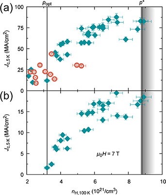
Figure 42. Dependence of Jc on charge carrier density: self-field inductive critical current density, Jc , at 5 K versus charge carrier density nH (100 K) in (a) self-field and (b) an applied magnetic field of 7 T of YBCO thin films obtained by CSD (red circles, 250 nm) and PLD (cyan diamonds, 200 nm). The critical current density is determined by SQUID magnetization measurements. Jc is strongly enhanced by increasing the charge carrier density far into the overdoped regime. Optimal and critical doping, popt and p*, are marked with vertical lines. Reproduced from [187]. CC BY 4.0.
Download figure:
Standard image High-resolution imageA more recent investigation directed to reach the OD state in REBCO films has been made by Miura et al [81]. In this study a thorough set of measurements were made, including carrier concentration in the normal state, penetration depth, Hc 2(T) and critical current density Jc (H) measurements. The study included pristine (Y,Gd)BCO and nanocomposite (Y,Gd)BCO-BHO thin films prepared by the low fluorine CSD approach and the carrier concentration was modified by oxygenating at different temperatures. Similar to Stangl et al [187], they reached the p* state and it was successfully confirmed that Jc sf is strongly enhanced (by a factor ≈ 1.4) as compared to the optimally doped state. Actually, record values in REBCO nanocomposite films (Jc sf (77 K)= 9 MA cm−2 and Jc sf (5 K) = 130 MA cm2) were demonstrated following a successful full oxygenation in samples having a large concentration of randomly distributed BHO NPs of small size (≈7 nm). This demonstrated that this nanostructural approach is very successful in creating a very attractive vortex pinning landscape, discarding that self-assembled nanostructures are required to reach very competitive CCs for high magnetic field applications (figure 43). Additional measurements of the magnetic field dependence Jc (H) and the pinning force Fp (H) also confirmed that record values are achieved at high magnetic fields (Fp max > 3 TN/m3 at 18 T and 4.2 K, see figure 43) so demonstrating the validity of the NPs approach to generate very efficient APC in REBCO films at low temperatures [81, 187].
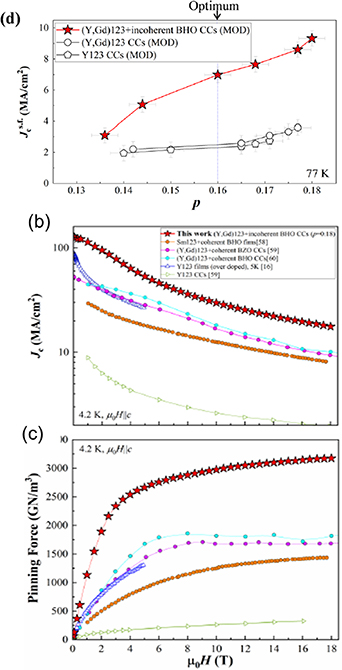
Figure 43. (a) Carrier concentration dependence p of self-field critical current density Jc sf at 77 K for standard (Y,Gd)123 and (Y,Gd)123 + BHO CCs grown by CSD; (b) magnetic field dependence of critical current density Jc (H||c) at 4.2 K; (c) pinning force Fp –μ0 H curve of overdoped (Y,Gd)123 + BHO CCs at 4.2 K and H||c. For comparison, the data for Sm123+ coherent BHO film 57, (Y,Gd)123 + coherent BZO CC58, (Y,Gd)123 + coherent BHO CC [271], overdoped Y123 film at 5 K [187], and Y123 CCs [300] are included. Reproduced from [81]. CC BY 4.0.
Download figure:
Standard image High-resolution imageThe main reason of reaching such strongly enhanced vortex pinning efficiencies in the OD state of REBCO is, as we have mentioned before, the increase of the condensation energy Ec. Recent measurements of Hc 2(p) when T ∼ 0 K in HTS allowed to calculate Ec (p) and demonstrate directly its enhancement when moving towards p* [245]. This means that, actually, the depairing critical current density Jd GL within the Ginzburg–Landau theory is also increased [81, 187, 301]:
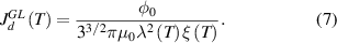
Simple heuristic arguments relating the critical velocity of Cooper pairs to the condensation energy per pair argued that Jd 2∝ nsEc , a relationship which has been experimentally validated (figure 44) [187]. On the other hand, through experimental determinations of λ(T) and ξ(T) in (Y,Gd)BCO films it can be estimated also that Jd GL increases by ≈30% when going from the optimally doped state popt to the critical point of the OD state p* [81].

Figure 44. Experimental verification of the proposed relationship Jc 2 ∝ nHEc , using Ec ∝ H0, where H0 is related to the vortex activation energy determined from magnetoresistance measurements and it is proportional to the pinning energy. The three parameters Jc, nH and Ec were derived experimentally from independent measurements. Reproduced from [187]. CC BY 4.0.
Download figure:
Standard image High-resolution imageRough estimations showed that following the overdoping approach the Jc/Jd GL ratio could be increased to reach ≈30% in pristine YBCO [187] and these results have been later confirmed in an extensive analysis performed in nanocomposite (Y,Gd)BCO films where it was shown that the Jc/Jd GL ratio remains ∼10% in OD pristine films, but it rises to ∼30% when NPs are added. The analysis of the thermodynamic effects governing the OD state was extended to several families of superconductors and it was suggested that the idea has a wide validity [81].
The underlying physics of the observed behavior in the normal and superconducting phases of the OD state when p* is approached, or beyond this value where superconductivity finally is suppressed, is continuously being investigated trying to unveil the mystery of the pairing in the cuprates [302, 303]. A very significant result is that there is no linear relationship upon doping (p) and the measured carrier concentration as determined through Hall effect carrier concentration measurements (nH ) [81, 187, 304, 305] and, as a consequence, the curve Tc (nH ) does not follow the characteristic parabola behavior of Tc (p), it rather saturates in the OD side (figure 45). The underlying reason of this anomalous behavior has been related to a Fermi surface reconstruction when the pseudogap closes at the critical point p* (from a Fermi surface having antinodal gap openings to a large cylindrical Fermi surface) which then shows a sudden increase of the carrier concentration encompassing an increase of the condensation energy (figure 45) [305–307].
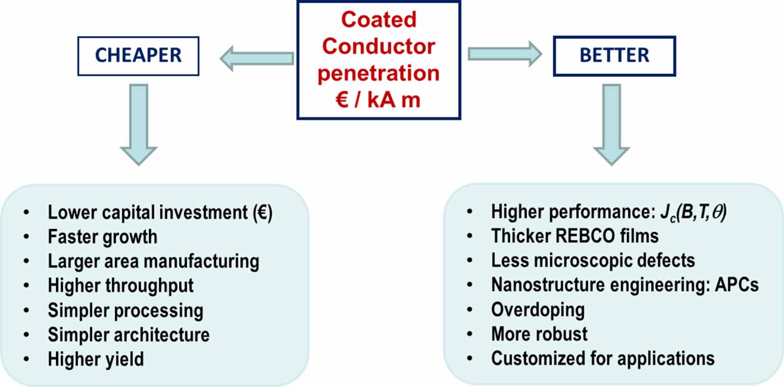
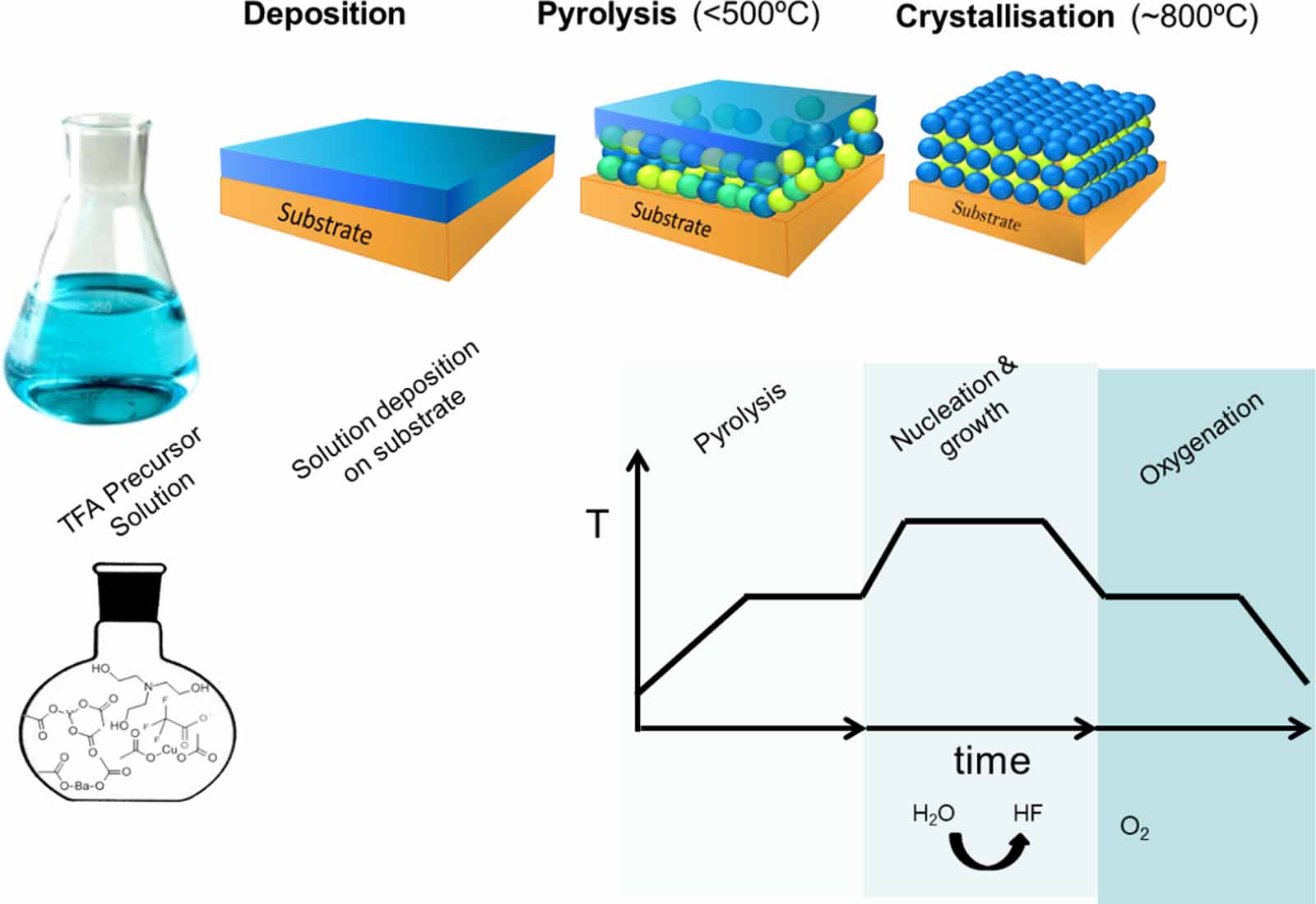
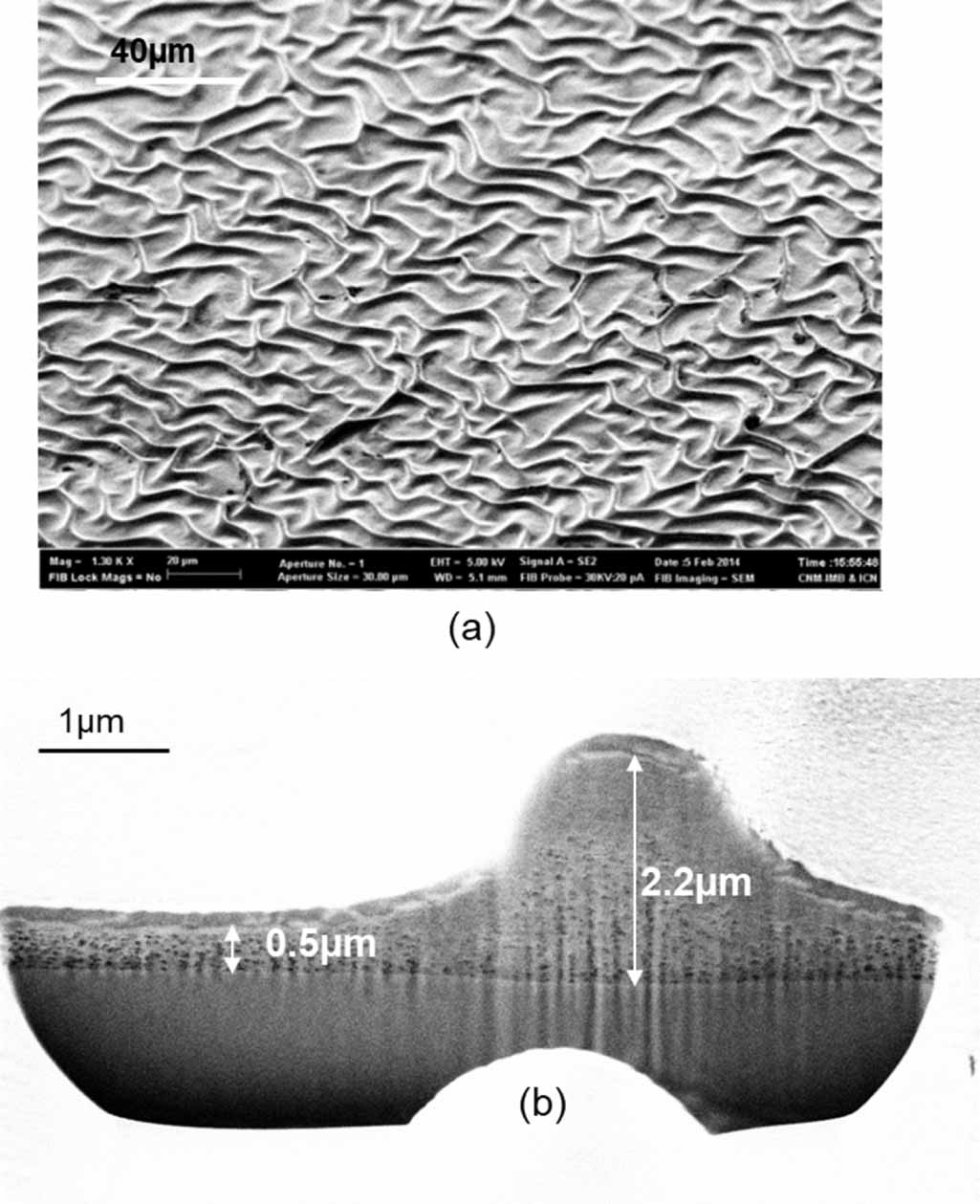
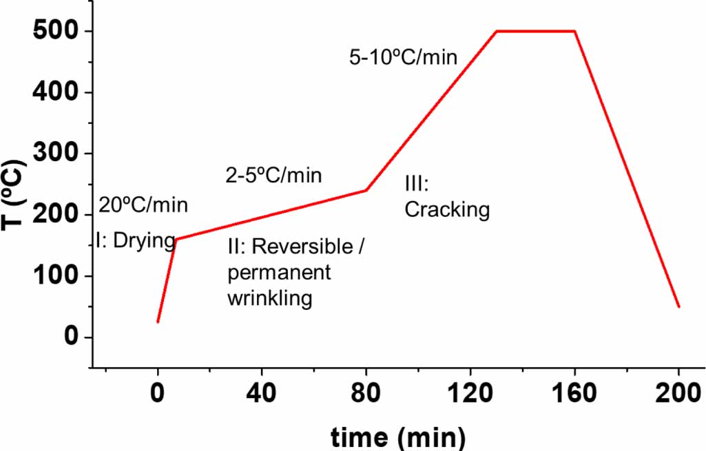
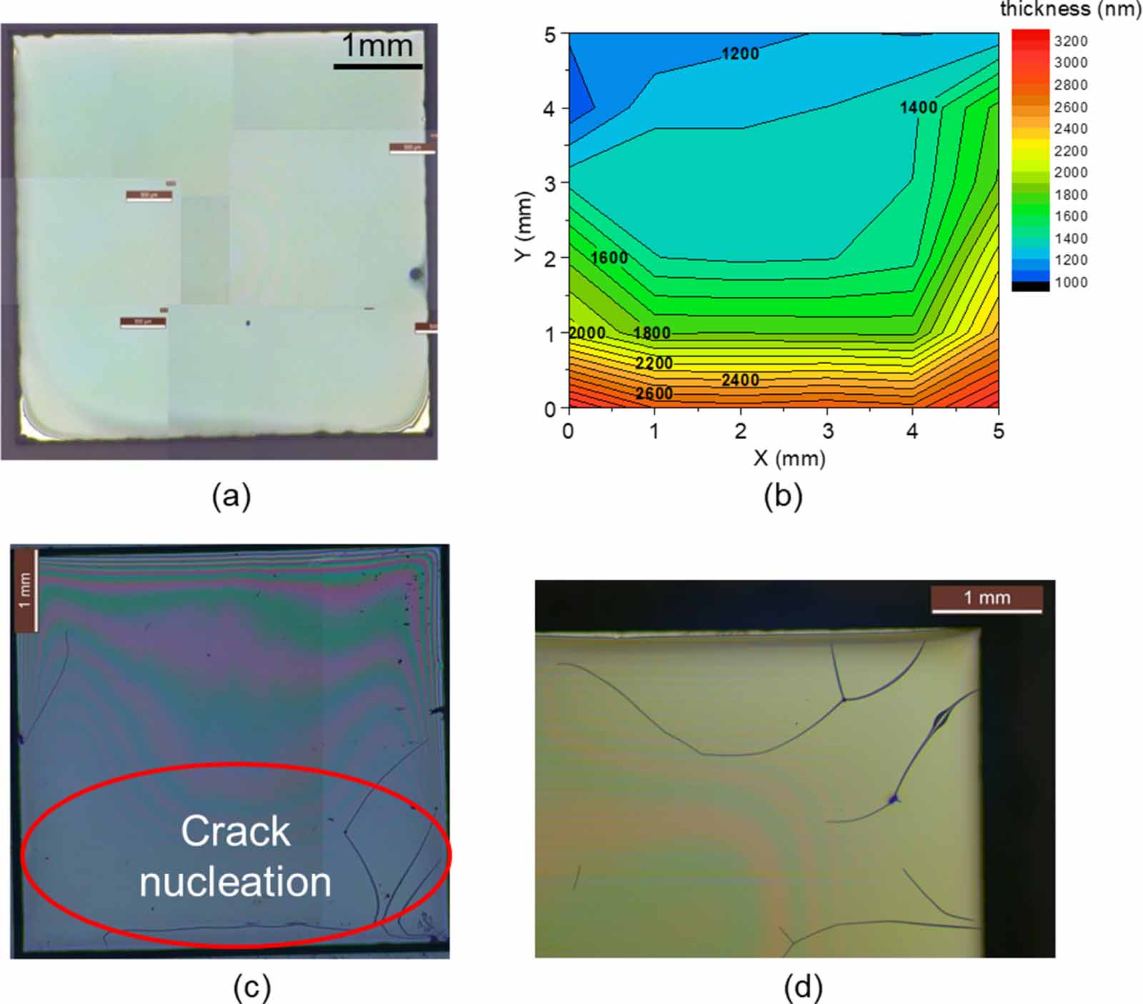
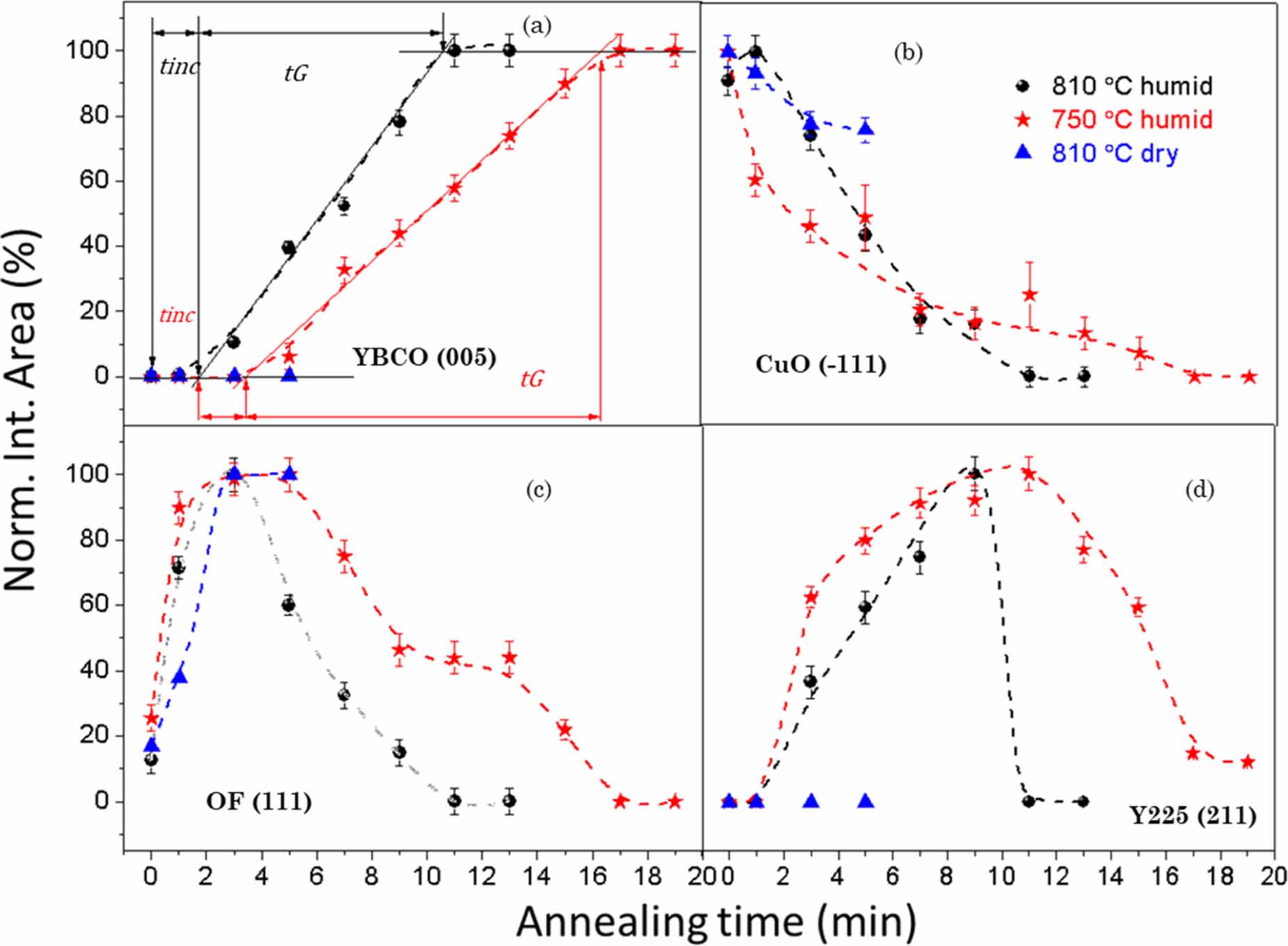
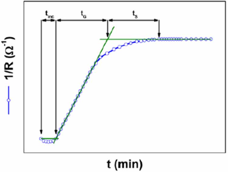
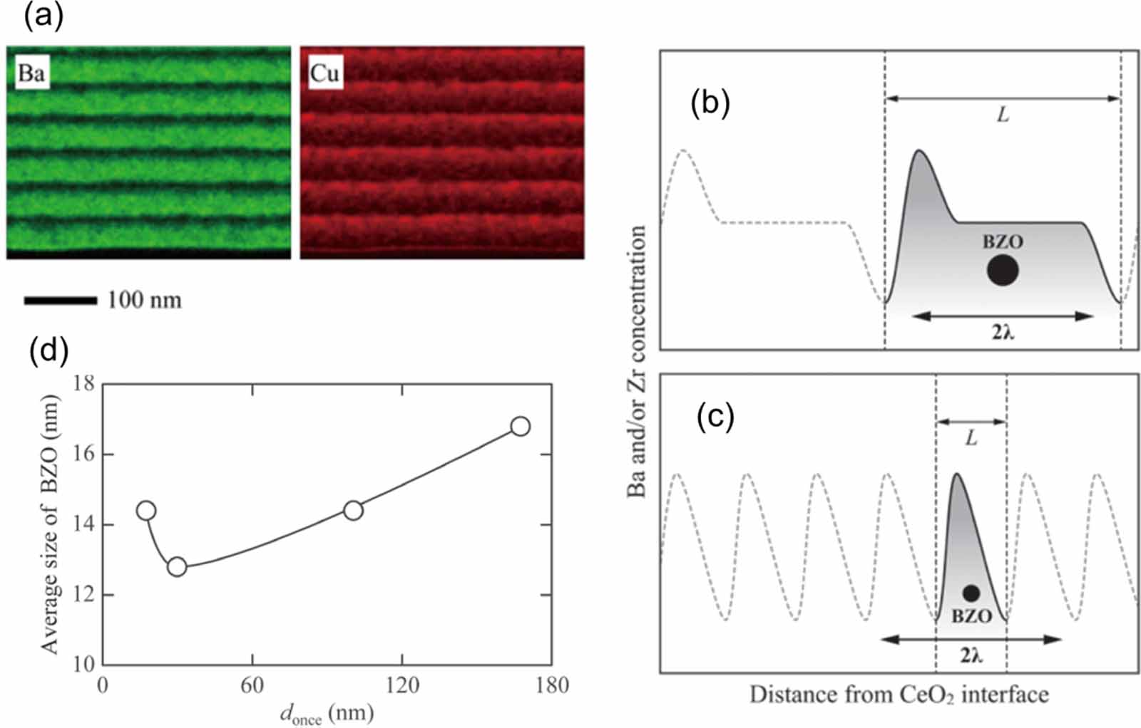
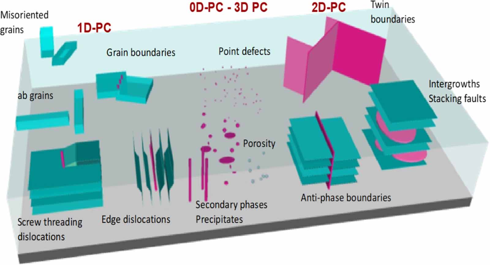
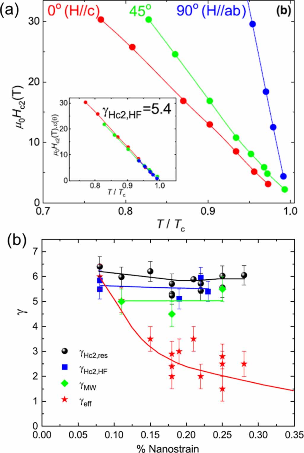
Figure 45. (a) Phase diagram of YBCO thin films. Zero field critical temperature as a function of charge carrier density, nH , obtained by Hall effect measurements at 100 K for thin YBCO films grown by PLD (200 nm thick, cyan diamonds) and CSD (250 nm thick, red circles). Vertical line marks optimally doping, while arrows indicate underdoped (UD) and overdoped (OD) regime. Inset magnifies Tc in the overdoped regime, showing a weak but distinct decrease with increasing charge carrier density, from above 91 K to around 89 K; (b) YBCO normal state charge carrier density per CuO2-plane, n, is drawn as a function of doping p. The charge carrier density is determined at 100 K. The doping p is obtained for optimally and overdoped samples (full symbols) via high resolution XRD measurements of the c-parameter and for underdoped films (open symbols) from the parabolic doping dependence of Tc . The vertical lines indicate optimally and critical doping. Below popt we find n= p, corresponding to a Fermi-surface with small hole and/or electron pockets in the underdoped regime (see inset). For p > p* a large, cylindrical Fermi surface is expected in the metallic overdoped regime (see inset), with n= 1 + p. A transition between a small and a large Fermi-surface occurs above p = 0.16. This is in good agreement with previous reports. Reproduced from [187]. CC BY 4.0.
Download figure:
Standard image High-resolution image
We should stress here that in the particular case of non-stoichiometric films (RE to Ba ratio 1:1.5) widely described before, it has been shown that an OD state may be reached achieving record values of superconducting performance [74, 76, 81]. Further investigation is required to clarify if the modified microstructure of these films promote the achievement of a higher oxygen content of the REBCO films.
In conclusion, there exists at present solid evidences of the outstanding superconducting performance for both pristine and nanocomposite REBCO films which can be achieved by choosing the OD state as the optimal composition. Although it is not an easy mission, it is worth persisting given the exceptional performances that can be reached. Therefore, a thorough study of the most appropriate compositions, nanostructures and oxygenation processes allowing to reach this state should be undertaken.
4.5. Scaling of CC manufacturing
For the sake of completeness, we would like to complete this review with a short summary of how far the extended knowledge generated on the use of fluorinated solutions to prepare CCs has been implemented at the industrial scale to produce long length conductors.
As we have previously summarized, the CSD route to CCs requires essentially three steps: 1/ solution preparation, 2/ solution deposition and pyrolysis and 3/ high temperature growth and oxygenation. Scaling-up these three steps has been the main objective of industrial producers in recent years and so now very significant throughputs are achieved in all the steps.
First of all, solution preparation of low fluorine metalorganic precursors is now widely controlled with the required volumes for long length conductor production, including a deep knowledge of the needed handling procedures to preserve a high quality, particularly to avoid any humidity related degradation [54]. We should remind here that the volume of metalorganic solution required to prepare a REBCO conductor with high superconducting critical current is in the range of one litter per km, i.e. a very acceptable consumable for any raw chemical industry. The composition of these starting solutions have also been tuned without any difficulty to that required to prepare nanocomposite films (including RE2O3, BaZrO3 or BaHfO3 NPs). The inorganic precursors to prepare the metalorganic salts are quite conventional and they may be produced at very affordable cost. Concerning the NP and colloidal solution production to prepare nanocomposite films through the multifunctional colloidal ink route, the processes described in section 2.2 are much more recent and only a few industrial producers have initiated a large scale production of them [103, 105, 308]. Actually, there exists quite extensive knowledge at industrial scale to produce large volumes of NPs and colloidal inks based on them and so it is not expected that scaling up this step should become a major barrier in its implementation for CC production.
The second step in the CSD route to CC production is the solution deposition and pyrolysis. At industrial scale the preferred solution deposition techniques are slot die coating or dip coating, although IJP has also been demonstrated and several different metallic substrates have been used, i.e. RABiT, IBAD and copper clad [29, 30, 146, 167, 172, 309–311]. The specific adaptation of composition to reach controlled rheological properties of the solutions have been widely implemented at the industrial scale to minimize the number of depositions. However, to reach high quality pyrolized films it is still required to perform quite slow heating processes and so pyrolysis could become a limiting step in the conductor throughput. To overcome this limitation, the industrial producers have devised multilane systems allowing to produce continuously the whole step (deposition and pyrolysis) and hence film thicknesses of several microns have been demonstrated. Additionally, these manufacturing systems may run continuously in an automatic mode with quite conventional low temperature (300 °C–500 °C) furnaces working at normal pressures and so they are not considered to be a relevant production barrier neither a cost limiter at present. This step could also be very easily extended to wider metallic substrates [310]. In conclusion, all the specific common steps related to the CSD approach have been widely implemented using non-vacuum technologies. These approaches are actually valid either for fluorinated and non-fluorine precursors to CCs [308].
The final step in CSD CC manufacturing is the growth of REBCO films through the BaF2 route, also including the final oxygenation process, two processes which have been widely discussed in previous sections. There exist several industrial producers which have implemented CSD CC manufacturing units producing lengths in the range of hundreds meters to one km [30, 63, 77, 172, 309, 312, 313]. Most of these systems use reel-to-reel units although some have also built batch furnaces adapted to coils of several hundred meters [63]. The main difficulty in designing the growth furnaces for the BaF2 process relies on the fact that, as we described in section 3.1, the formation of REBCO is a solid–solid reaction where the kinetics is controlled by the gas pressure at the epitaxial growing interface, i.e. PH2O and PHF. For that reason, it is crucial to avoid any HF gas stagnancy which would slow down the reaction rate and so further reduce the growth rate and create film inhomogeneities. This issue was mainly solved through the design of transverse gas flow architectures with a tight control of the gas flow assuring that the HF exhaust gas is fully eliminated [314, 315]. It is certainly a major drawback, however, to implement such a complex gas control system when we need to increase the width of the tapes. Even though, several producers have implemented multilane growth furnaces to cope with this limitation [149]. There exist a quite extended range of temperatures, PO2 and PT conditions which have been used depending on the cap layer of the substrate, the RE ion, the film thickness and the NP content. In all cases, however, the REBCO growth rate remains quite low thus limiting the throughput of the BaF2 process because then it requires quite extended high temperature annealing times or long furnaces. Concerning the demonstrated superconducting performance, several producers have already demonstrated Ic values at 77 K in the range of 400–500 A cm−1-w with lengths of 300–1.000 m and a fairly good homogeneity [30, 63, 172, 316]. The CSD CCs are already being considered a competitive industrial product and so they are being implemented in power devices such as cables. The performances achieved at high magnetic fields and low temperatures, where vortex pinning needs to be optimized, are also outstanding. The critical current density record values demonstrated at the laboratory scale have not yet been transferred to long length conductors and so further development is required [40, 81, 312].
To conclude, as we mentioned in the Introduction and scope section, the CSD approach has the advantage of requiring a relatively low CAPEX to implement the manufacturing units, as well as limited operating costs [317]. Therefore, even if there still remains several aspects which require further development, the CSD approach to CCs has a brilliant future ahead [318].
5. Conclusions and outlook
The present review has been focused on the progress of all the aspects related to the preparation, nanostructure and superconducting properties of REBCO thin films and CCs grown by CSD using fluorinated metalorganic precursors. As it was mentioned in the Introduction section, although more than 34 years have been elapsed since the first demonstration that these precursors could be properly used to grow epitaxial films, the generation of a great deal of knowledge was still necessary at that time before this approach could become a reliable and high throughput route to CCs. The more recent reviews about the advancements on the route of fluorinated precursors to grow REBCO films and CCs were published more than 11 years ago [20, 28], while extended new knowledge about this topic has been generated during this period, therefore, we are convinced that the preparation of the present progress review was fully justified.
This review first focuses on the common principles of the CSD technique, i.e. the metalorganic precursor solutions, the colloidal NPs preparation, the solution deposition, the pyrolysis process and the evolution of the intermediate inorganic precursors phases while heating to the growth temperature once the pyrolysis is completed. The use of low-fluorine content precursors was widely accepted owing to its reduced environmental impact (reduced use of fluorine containing compounds) and process reliability (reduced hygroscopic behavior of the solutions) and it did not actually deeply modify the whole process. On the other hand, the advances in understanding the physico-chemical behavior of the solutions and the metalorganic precursors once deposited on the substrates and during the pyrolysis has been outstanding, mainly because new kinetic insights were made through the use of in-situ analytical tools. We know now much more about the physico-chemical transformations and the kinetics of the pyrolysis process and it has been particularly clarified at which temperature stages the solvent evaporates, and when film wrinkling and cracking may occur and which roles plays the propionate and TFA molecules within the bonding skeleton. These analyses are crucial to increase the maximum film thickness which can be achieved with a single deposition (∼1 μm) while keeping a homogeneous film at the macroscopic scale (no wrinkling and no cracks). Of course, it has been confirmed as well that multideposition is a very viable strategy to increase the total film thickness by CSD because a high nanoscale homogeneity is preserved.
The deepest advances related to the preparation of precursors have been made, however, in relationship to the approaches followed to prepare nanocomposite films. It was first shown under which conditions a tight control of the size and distribution of the precursors secondary phase NPs is kept. The same conditions are needed for the secondary phases expected to behave as APCs, obtained either by using the SS approach (complex metalorganic precursors and growth process) or the new route based on the use of preformed oxide NPs. The preformed NPs could be prepared following solvothermal methodologies, which may lead to stable colloidal solutions with high NP concentrations while keeping them well dispersed even with very small sizes (5–7 nm). The multifunctional colloidal methodology had never been used before within the CSD route to prepare nanocomposites and so it took quite a while to find the right solvents, additives and experimental methodologies as well as the suitable NP compositions. It was required to reach a tight control of the oxide NPs size, to keep them stable and non-aggregated for a long time and, finally, to reach multifunctional ink compositions which can be used as precursors to grow REBCO nanocomposite films. The most suitable oxide NPs have been shown to be BaMO3 (M = Zr, Hf) perovskites because they are not reactive with the REBCO precursors, although ZrO2 or HfO2 fluorites could also lead to reasonable nanocomposites when they react with the Ba precursors and also lead to the formation of BaMO3 (M = Zr, Hf) perovskites.
Once it was demonstrated that the multifunctional colloids were stable and lead to homogeneous pyrolyzed films, it was necessary also to ascertain that they remain stable during the heating process, i.e. they keep the initial size and homogeneous distribution. For that reason, the evolution of the intermediate phases was investigated when heating from room temperature to the nucleation and growth temperatures, once the films have been pyrolyzed. Here it was discerned that the CTA (heating rate of ∼25 °C min−1) leads to a sizeable coarsening of the intermediate NP precursors and secondary NPs, while the new FH process (30 times faster), completely eliminated the coarsening process and keeps the nanoscale homogeneity.
But the real 'tour de force' is to reach a complete control of the nucleation and growth processes, of both the REBCO pristine and nanocomposite films and these steps have been further analyzed in much more detail in recent years. First of all, additional knowledge about nucleation control on pristine thick films (∼1 μm) was generated together with disentangling the temperature dependence of YBCO growth rate which remains rather low (∼1 nm s). The kinetics of the oxygenation process of YBCO was also revised and it was concluded that the surface exchange step is the slowest one in thin films. Very significant new knowledge has been generated about the nucleation and growth processes of nanocomposites, both those based on SS and those based on multifunctional colloidal solutions. In the first case, the main success was to show that the NPs can nucleate homogeneously at lower temperatures than REBCO films and so nanocomposites with randomly oriented small NPs embedded in the matrix are achieved, although it is quite cumbersome to control its growth rate. To overcome this nuisance, a novel strategy was created (UTOC) which is able to keep small particle sizes even at high concentrations. In the colloidal route to nanocomposites it was also clear that the preformed NPs essentially keep their size and so the nanocomposite growth is facilitated because a single set of annealing conditions leads to very homogeneous films. The most outstanding combination has been shown to be REBCO-BMO (M = Zr, Hf) in both cases.
The final convincing demonstration of the competitiveness of the CSD route to high performance REBCO CCs arises from the extensive investigation performed to correlate the nanostructure with the achieved critical currents. Thorough micro/nanostructural studies have been performed to stress which defects are relevant at different length scales. On one side, in order to maximize the self-field critical current density, it was clear that the extent of the percolating paths should be maximized avoiding that large NPs, voids, pores or high angle grain boundaries remain in the films. On the other hand, to control the vortex pinning landscape it was crucial to investigate, mainly by STEM-EELS, the atomic scale structure of the pre-existing defects, such as SFs and TBs, and how these defects interact with the secondary phase NPs. Owing to the fact that the NPs are randomly oriented their interface with the matrix is a source of additional SF generation and so the nanocomposite films display a huge concentration of short SFs which can be easily quantified through x-ray diffraction nanostrain measurements.
It was also very remarkable that a unique atomic defect structure of the SFs was described where clusters of Cu vacancies decorated with O vacancies exist and this is the reason of preserving the global Y:Ba:Cu atomic stoichiometry, even if the SF concentration is very high. These SFs are, therefore, a very relevant source of point and extended defects (partial dislocations surrounding them) which play a key role in defining the vortex pinning landscape. They also influence the coherence along the c-axis of the TBs which are perturbed by the SFs. A novel mechanism correlating nanostrain with the generation of APCs in the REBCO matrix has been suggested to explain the key role of SFs.
The most successful recent methodologies to correlate vortex pinning efficiency at different temperatures, magnetic fields and magnetic field orientation have been reviewed stressing the useful parameters to characterize the single vortex pinning regime at low fields and the collective vortex pinning regimes at high fields. The single vortex pinning step is characterized by the accommodation field H*. The evolution of this parameter clearly supported the conclusion that the NPs contribute, in addition to the SFs, to enhance the vortex pinning strength. The systematic analysis of the Jc (T,H,θ) dependencies in many different compounds has allowed to discern which defects play a key role as isotropic-strong, anisotropic-strong and isotropic-weak pinning and so being able to schematize the vortex pinning landscape in the whole H–T phase diagram, and the regions where very competitive pinning forces are achieved were identified.
Last but not least, recent efforts to look for alternative routes to maximizing the critical currents, we have stressed several works showing the outstanding role played by the enhancement of the condensation energy of REBCO compositions in the OD state, particularly at the critical point of carrier concentration p* where the pseudogap of REBCO closes. Through the implementation of adapted oxygenation processes an increase of the carrier concentrations was demonstrated, which lead to the highest values of critical current densities achieved so far in any REBCO pristine and nanocomposite films and CCs, including other deposition techniques. This shows that the nanostructure based on random NPs has the capability of reaching the highest performances of CCs including those generating self-assembled nanostructures, as in the case of in-situ grown REBCO nanocomposite films. We conclude with a summary of how the generated knowledge has been transferred to the large scale manufacturing of CCs.
As an outlook concerning the future capabilities of the CSD route to prepare competitive large scale CCs we are convinced that the demonstrated advances concerning all the steps related to the procurement of precursor films (solution and NP preparation, solution deposition, pyrolysis and pre-heating) have already deeply anchored principles and thus they must be considered mature methodologies suitable for large scale industrial manufacturing while keeping the great attractiveness of being an approach characterized by low CAPEX. All these steps are actually fully compatible with any other CSD precursors alternatives, such as those based on non-fluorine metalorganic precursors mentioned before, which are based on a completely different growth reaction to form REBCO films.
This remark is very important because, as we have mentioned before, one of the main concerns mentioned in this review related to the CSD route of REBCO films based on fluorinated precursors has been the difficulties to enhance the growth rate of the gas-controlled solid–solid reaction based on BaF2 as an intermediate compound to grow YBCO. This limits the CC production throughput and requires complex furnaces design to extend at larger widths the CC production. These features have been identified as a limitation for a competitive industrial future of the classical fluorinated CSD approach. Fortunately, modified novel CSD approaches have recently demonstrated that non-fluorinated multifunctional colloidal precursors grown by TLAG leads to ultrafast growth rates (more than three orders of magnitude faster) keeping high superconducting performances. This overcomes the main difficulty of achieving a high throughput CSD CC production with high superconducting performance and a low CAPEX and so with the expectance of a strong decrease of the figure of merit cost/performance.
Acknowledgments
Authors acknowledge the European Union Research Council for EUROTAPES (EU-FP7-NMP-LA-2012-280432) and FASTGRID (EU-H2020, 721019) projects and EU COST actions OPERA (CA20116) and SUPERQUMAP (CA-21144); the European Research Council for ULTRASUPERTAPE (ERC-2014-ADG-669504), IMPACT (ERC-2019-PoC-8749) and SMS-INKS (ERC-2022-PoC-101081998) projects. Also acknowledged is the financial support from the Spanish Ministry of Science and Innovation and the European Regional Development Fund, MCIU/AEI/FEDER for COACHSUPENERGY project (MAT2014-51778-C2-1-R and MAT2014-51778-C2-2-R), SuMaTe (RTI2018-095853-B-C21 and RTI2018-095853-B-C22), SUPERENERTECH (PID2021-127297OB-C21, PID2021-127297OB-C22) and PID2022-138492NB-I00, FUNMAT and FUNFUTURE ICMAB 'Severo Ochoa' Program for Centers of Excellence in R&D (SEV-2015-0496, CEX2019-000917-S) and HTS-JOINTS (PDC2022-133208-I00). They also thank the PTI+ TransEner CSIC program for Spanish NGEU (Regulation (EU) 2020/2094) and Catalan Government for 2017 SGR 1519 and 2021 SGR 00440 and that of Aragon for RASMIA (E12-23R).
Data availability statement
No new data were created or analyzed in this study.