

Abstract
In recent years Bi2Sr2CaCu2Ox (Bi-2212) received increasing attention due to its round wire multifilamentary architecture, a unique feature in high-Tc superconductor. In fact, round wires are preferable for magnet designs, including solenoids for nuclear magnetic resonance (NMR) or research purpose and accelerator magnets. However, due to the narrow over-pressure heat treatment conditions necessary to obtain high Jc and to the peculiar microstructure of Bi-2212 wires, a full understanding of the correlations between the different properties has not yet been developed. In this paper we investigate the effect of a vital part of Bi-2212 optimization, the maximum heat-treatment temperature Tmax in the range of 885 °C–896 °C, on the variations of Jc, effective filament diameter deff, anisotropy γ, INTER- and intra-grain irreversibility fields and pinning energies U0, all critical parameters in unravelling the complex mix of vortex pinning and connectivity that ultimately determines the critical current density. We found that deff of the higher Jc wires heat-treated at lower temperature is much smaller than for the lower Jc wires. Moreover, a systematic increase of the irreversibility field and a decrease of the intrinsic Bi-2212 anisotropy underpins the higher Jc. The analysis of the pinning energies reveals that there is little sample-to-sample variation in the INTER-grain pinning, whereas in all samples the intra-grain pinning has an enhancement below ∼40–45 K becoming more and more evident with increasing Jc. These results suggest that the overall Jc performance are not only related to the wire microstructure and connectivity, which obviously affect the INTER-grain properties, but they are also intimately related to the intrinsic and intra-grain properties such as γ and U0.
Export citation and abstract BibTeX RIS

Original content from this work may be used under the terms of the Creative Commons Attribution 4.0 license. Any further distribution of this work must maintain attribution to the author(s) and the title of the work, journal citation and DOI.
1. Introduction
Bi2Sr2CaCu2Ox (Bi-2212) is one of the most promising high temperature superconductors (HTSs) for high field applications [1]. In fact, Bi-2212 wire is the only HTS round conductor. It is also made in kilometre-piece length with a relatively simple powder-in-tube (PIT) multifilamentary design [2, 3] suitable for the realization of accelerator and research magnets at fields larger than 20 T [4–7]. To achieve its best performance, Bi-2212 wire has to undergo an overpressure heat treatment (OPHT) with multiple steps and multiple parameters, which affect both the microstructure and transport critical current density (Jc ) [1, 8, 9]. It was recently showed that the quality of the precursor powder has a significant effect on the wire performance and on the narrow processing window on Bi-2212 [10, 11]. An important factor in understanding Jc defined by Ic /Afil is that in unreacted wires the filaments are not fully dense, with the powders typically occupying 2/3 of the filament cross-section and the balance being trapped gas, typically air. Although mechanical deformation can reduce the volume of gas trapped in the PIT wire [12, 13], OPHT processing hydrostatically shrinks the gas bubbles in the wire to almost zero, greatly preventing the bubbles from compromising the filament connectivity [1, 14, 15]. In OPHT wires, the filament cross-section is estimated after densification, making Jc = Ic /Afil ∼ Ic /ABi-2212. Another important factor is that heat treating short Bi-2212 round samples without overpressure leads to large effective filament diameter, deff, exceeding the bundle diameter, dBundle [16].
The microstructure of reacted Bi-2212 wire has a few peculiar and distinctive features. The first is a vital local biaxial texture in which Bi-2212 grains with a strongly aligned crystallographic a-axis develops along the wire longitudinal axis [17]. This assures a relatively small grain-to-grain misorientation (FWHM < 10° in high-Jc wires) with high grain boundary connectivity essential to large Jc . Since the wire is made of more than thousand filaments and because of the rotation along the filament length of the local c-axis direction, the macroscopic Bi-2212 wire properties are isotropic despite the high anisotropy (γ) of the individual Bi-2212 grains. A second feature is the presence of Bi-2212 filament 'bridges' through the silver matrix [18]: these Bi-2212 bridges outgrow the initial filaments during the partial melt connecting some of the filaments in the bundle. Depending on the wire architecture (e.g. filament distance) and heat treatment (HT) conditions, these connections can actually develop from random angle impingement into actual filament merging with common grains. The benefits and detriments of these inter-filament connections is not fully clear: filament merging seems to be mostly detrimental causing a worsening of the biaxial texture, whereas conceptually some filament bridging could be beneficial because it generates additional paths for supercurrent flow, which might bypass current blockages.
One of the key OPHT parameters is the maximum HT temperature Tmax (typically set in the 885 °C–896 °C range), which also directly affects the time in the melt tmelt. In fact tmelt is defined as t872 °C↓–t884 °C↑, where t884 °C↑ and t872 °C↓ are respectively the times at which Bi-2212 starts melting on heating and starts solidifying on cooling [8, 9, 19]. In this step, together with Bi-2212 powder particles melting, there is also some dissolution of Ag from the sheath and penetration of liquid along Ag grain boundaries, which allow filament bridging to occur. This makes tmelt a vital parameter in evaluating the final Jc . Jiang et al demonstrated that, despite property variations caused by wire design or diameter, and quality of the precursor powers, Jc generally reaches its maximum for the lowest possible Tmax that allows full melting. At higher Tmax there is a lower-Jc plateau or one with a moderate decrease up to ∼896 °C [8]. At the lowest Tmax having maximum Jc there is only limited filament bridging, but with increasing Tmax significant inter-filament connective bridges develop. These are the features of the wire investigated here. The cross-sections of the samples in the present paper were recently characterized by scanning electron microscopy (similar to that in [8]) and by extensive x-ray diffraction to evaluate their grain texture [20], which revealed a systematic worsening of the [100] Bi-2212 texture with increasing Tmax.
Some of the driving questions for this study of Bi-2212 wires are: Does 2212 show signs of granularity despite its good overall Jc performance? Is there evidence of multiple scales of current flow? How does the irreversibility line vary, and can we tune it? How are variations of vortex pinning affecting the overall Jc performance? Answers to these questions are vital to understanding what really controls current flow and thus the macroscopic Jc . In our previous study [21] we demonstrated that detailed magnetic characterizations can provide useful information for answering some of these questions. For instance, using AC susceptibility we demonstrated that in moderate and low-Jc samples (∼5200–4200 A mm−2 at 5 T and 4.2 K, obtained by varying the HT cooling rate) there was evidence of separate intra- and INTER-grain currents with different irreversibility lines and evidence for variable vortex pinning performance. In this paper we are now investigating the properties of higher-Jc samples (∼7100–5100 A mm−2 at 5 T and 4.2 K) in order to understand which are the key features that lead to the best performance.
2. Methods
The Bi-2212 conductor used in this work is an 85 × 18 restack design (pmm180410) constituted of 18 bundles with 85 filaments each, for a total of 1530 filaments. The Bi-2212 precursor is made of Engi-Mat powder (LXB116). The wire diameter was 1 mm, reaching an averaged densified filament diameter prior to melting of ∼11.2 µm. Three samples underwent the typical OPHT described for instance in [9, 19] reaching maximum temperatures, Tmax, of 885 °C, 887.5 °C and 896 °C.
The critical current was measured in transport at 4.2 K up to 15 T as reported in [20], finding that the engineering current density JE and so the critical current density Jc have a clear variation with Tmax, similarly to what previously reported on the same conductor in [8]. The maximum Jc is obtained at the lowest Tmax = 885 °C reaching 7115 A mm−2 at 5 T and 4.2 K. With a small increase of Tmax (887.5 °C) Jc drops at 5565 A mm−2 and then it almost plateaus reaching 5085 A mm−2 at 896 °C. These properties are summarized in table 1 and, in the following the samples will be identified by Tmax and/or their Jc (5 T).
Table 1. Heat treatment temperature, superconducting properties, effective filament diameter also normalized to the bundle size and intra-bundle connectivity for the 3 investigated Bi-2212 wires. Columns reporting ranges of value refer to the variations in the measured field range.
| Tmax °C | Jc (5 T, 4.2 K) A mm−2 | JE (5 T,4.2 K) A mm−2 | Jc (15 T, 4.2 K) A mm−2 | JE (15 T,4.2 K) A mm−2 | deff µm | deff/dBundle | γ2,Bundle | µ0 HK (20 K) T |
|---|---|---|---|---|---|---|---|---|
| 885 | 7115 | 1430 | 5145 | 1035 | 56–59 | 35%–37% | 8.3%–9.0% | 8.95 |
| 887.5 | 5565 | 1120 | 4095 | 825 | 88–99 | 55%–62% | 14.5%–16.5% | 8.78 |
| 896 | 5085 | 1020 | 3795 | 765 | 85–98 | 51%–59% | 14.1%–16.6% | 8.54 |
All magnetic characterisations were performed with field perpendicular to the wire axis, which is the most relevant to investigating properties related to the transport performance, using samples about 4 mm in length. The superconducting transitions were obtained by DC magnetization in a Quantum Design (QD) MPMS-5 SQUID magnetometer applying 1 mT to estimate the average bundle size [21]. Hysteresis loops were evaluated in a QD 16 T PPMS using a vibrating sample magnetometer (VSM), with a ramp rate of 0.462 T min−1, in a temperature range between 4.2 and 45 K to evaluate the effective filament diameter deff at 4.2 K and to obtain the Kramer plots and their extrapolations, HK
. AC susceptibility was performed in a QD 9 T PPMS varying µ0
Hac
between 0.1 and 1.5 mT, µ0
HDC
between 0 and 9 T and the frequency from 13 to 211 Hz [22, 23]. This characterization allows us to separate the intra and INTER-grain contributions and, analysing the AC amplitude and frequency dependences of the first harmonic  peaks, to determine the corresponding irreversibility lines and pinning energies. The details of this approach are described in [21] and references within.
3. Results and analysis
3.1. Low-field DC magnetization
Figure 1 shows the superconducting transition for the three wires obtained after zero-field cooling. These data reveal that changing Tmax has small effect on Tc and the transition width in this field configuration. Taking into account the demagnetization factor for samples of cylindrical shape, in the top panel we assumed that the relevant diameter is the single Bi-2212 filament. As already demonstrated in [21], this assumption is, however, incorrect leading to an unphysical χfil value at low temperature of about −1.4. This can be explained only by screening current being induced on volumes larger than the filaments, an effect caused by the significant filament bridging in Bi-2212 wires. Because of the peculiar microstructure, imposing a low-temperature limit of −1 and back-calculating the size, we demonstrated that the relevant diameter is the bundle size. In fact, we estimated for these samples a dBundle ranging from 158 to 165 µm, compatible with the microstructurally estimated values. These dBundle values will be used in the following characterizations.

Figure 1. (a) Temperature dependence of χfil estimated by DC magnetization after zero-field cooling, calculated assuming that the relevant size is the filament diameter. (b) The same data re-analysed as χBundle, i.e. imposing a value of −1 at the lowest temperature in order to back-calculate the bundle size (see explanation in the main text).
Download figure:
Standard image High-resolution image3.2. Effective filament diameter and Kramer analysis
In addition to the transport Jc
(4.2 K) characterizations [20], we also performed hysteresis loop measurements to evaluate the effect of Tmax on the effective filament diameter and its field dependence. deff was calculated through the usual relation  (SI units) with △M being the amplitude of the hysteresis loop of the superconducting phase and Jc,t
the critical current density obtained in transport [16, 24].
(SI units) with △M being the amplitude of the hysteresis loop of the superconducting phase and Jc,t
the critical current density obtained in transport [16, 24].
We found that the higher Jc
wire (Tmax = 885 °C) has the smallest deff at 4.2 K, with deff varying from 59 to 56 µm in the 3–15 T range, which corresponds to 35%–37% of the bundle diameter (figure 2). The lower Jc
samples have much large deff (99–88 µm and 98–85 µm for Tmax of 887.5 °C and 896 °C, respectively), clearly larger than 50% of dBundle, and with a stronger in-field variation (table 1). Obviously, most of the sample-to-sample difference of deff is caused by the magnitude of the transport Jc
. However, we also observed that the deff field-dependence becomes stronger with decreasing Jc
. Both magnetization and transport data yielded power laws,  and
and  but we did observe that there is a significant difference in both the absolute values of α and their trends with respect to the wire Jc
(figure 3(a)). α obtained by magnetization is always larger than that by transport measurements. Moreover, the difference between αm
and αt
decreases with increasing wire Jc
, clearly causing the more marked field dependence of deff for the lower-Jc
samples as seen in figure 2 (
but we did observe that there is a significant difference in both the absolute values of α and their trends with respect to the wire Jc
(figure 3(a)). α obtained by magnetization is always larger than that by transport measurements. Moreover, the difference between αm
and αt
decreases with increasing wire Jc
, clearly causing the more marked field dependence of deff for the lower-Jc
samples as seen in figure 2 ( ). Although some of the differences in the α-values can be caused by the different electric field in the transport and magnetization characterizations, most of it is likely related to the different bridging level, microstructure and the consequent current percolation paths involved in the two techniques (see section 4).

Figure 2. (a) Effective filament diameter, deff, at 4.2 K and (b) deff normalized to the bundle diameter, dBundle, as a function of magnetic field.
Download figure:
Standard image High-resolution image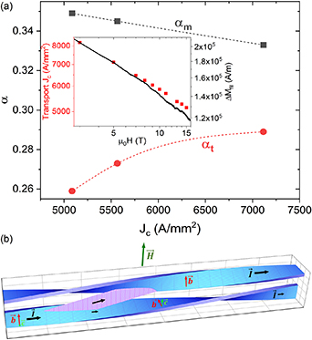
Figure 3. (a) α values obtained from the  and
and  relations for both transport and magnetization characterizations. In the inset the field dependence of the transport and magnetization data for the highest Jc wire. (b) Sketch representing the transport current transferring from one filament to another in 2212 wires: the blue elements represent the local filament orientation averaged over the grains within the filament, schematically showing the rotation of the averaged c-axis direction along the filaments; the magenta transversal element represents an inter-filament bridge.
Download figure:
Standard image High-resolution imageHysteresis loops were also performed at higher temperature to verify the evolution of the Kramer field with temperature (figure 4) and to compare the samples. In Bi-2212 a standard Kramer extrapolation cannot be performed because the plots do not show a linear trend at high field approaching the irreversibility field. This is presumably caused by the presence of multiple pinning mechanisms [25, 26] and by the material anisotropy with current percolating through grains with some degree of misorientation with respect to the field. Despite the lack of high-field linearity, in this material a Kramer extrapolation (for instance at 20 K) is frequently performed in the almost linear region at intermediate-field as a way to compare different samples [8]. The Kramer extrapolation at 20 K, reported in table 1, shows that HK progressively decreases with decreasing Jc . Figure 4 also reveals that, when the Kramer plots at different temperature are normalized to the linear trends used to estimate Hk , the high-field tails substantially overlap suggesting the high-field/low- temperature pinning mechanism does not significantly change. Further discussion will be given in section 4.

Figure 4. (a) Kramer plot in the 4.2–45 K range for the wire with Jc (4.2 K,5 T) of 7115 A mm−2 with the linear extrapolations from the intermediate-field regions to determine HK . (b) Same data of above panel normalized to the respective linear trends.
Download figure:
Standard image High-resolution image3.3. AC susceptibility
As mentioned above, AC susceptibility can be used to determine sign of granularity or weak connectivity in superconductors [27, 28] and we have recently demonstrated that this approach can be used also to evaluate the properties of Bi-2212 round wires (see [21] for detailed explanations about the analysis procedure and contribution identifications). Figure 5 shows an example of AC susceptibility measurements, performed with an AC field of 1 mT at 73 Hz, on one of the Bi-2212 wires investigated here. The real part  shows some evidence of double diamagnetic transitions that become more obvious with increasing DC field, whereas the dissipative peaks
  reveal unusual shapes with an enhancement on the high-temperature side of the peak. This is due to the overlapping of two peaks as emphasized in figure 6, where we report the
  data at 9 T fitted by a double-Gaussian function above a linear background (the errors in the evaluation of the peak positions are smaller than the symbol size; they are typically less than 0.1 K, sometimes increasing to ∼0.3 K for the wider and smaller high-temperature peaks). The double diamagnetic transition and the double peaks are caused by intra-grain (at higher temperature) and INTER-grain (at lower temperature) contributions. From the
  analysis we can determine the peak positions by varying the Hac
amplitude and the frequency. Since Jc
is proportional to Hac
, investigating the shift of the
analysis we can determine the peak positions by varying the Hac
amplitude and the frequency. Since Jc
is proportional to Hac
, investigating the shift of the  peak as a function of Hac
, the irreversibility line (defined by the condition Jc
= 0) can be determined as the limit of the peak position for Hac
→ 0 [29, 30]. On the other hand, analysing the peak shift with changing frequency enables the pinning energy U0 to be evaluated by the relation
peak as a function of Hac
, the irreversibility line (defined by the condition Jc
= 0) can be determined as the limit of the peak position for Hac
→ 0 [29, 30]. On the other hand, analysing the peak shift with changing frequency enables the pinning energy U0 to be evaluated by the relation  by using the Arrhenius plots ln(f) versus 1/Tp
(f0 is the characteristic frequency and Tp
the peak position) [31]. Because of these double peaks, we will be able to evaluate both the intra-grain and INTER-grain properties.
by using the Arrhenius plots ln(f) versus 1/Tp
(f0 is the characteristic frequency and Tp
the peak position) [31]. Because of these double peaks, we will be able to evaluate both the intra-grain and INTER-grain properties.

Figure 5. Temperature dependence of the AC susceptibility evaluated on the bundle size for the higher Jc
Bi-2212 wire measured with µ0
Hac
= 1 mT at 73 Hz and with increasing DC-fields up to 9 T as indicated by labels near the dissipative peaks (H┴wire).  shows a double diamagnetic transition and
  reveals an anomalous broadening on the high-temperature side of the dissipation peaks.
Download figure:
Standard image High-resolution image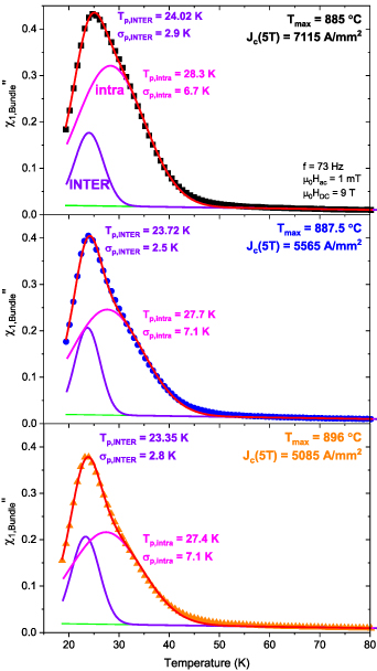
Figure 6. Comparison of the dissipative peaks  at 9 T for the three wires, including the analysis with the 2-Gaussian fits, showing an obvious variation of the higher temperature intra-grain peak (Tp
,intra). The shown data are taken at µ0
Hac
= 1 mT and 73 Hz.
at 9 T for the three wires, including the analysis with the 2-Gaussian fits, showing an obvious variation of the higher temperature intra-grain peak (Tp
,intra). The shown data are taken at µ0
Hac
= 1 mT and 73 Hz.
Download figure:
Standard image High-resolution image3.3.1. Irreversibility lines.
From the INTER- and intra-grain Tp versus Hac plots, the irreversibility temperature TIrr was extrapolated for each DC field. The obtained irreversibility lines are reported in figure 7, showing a clear separation between the INTER- and intra-grain irreversibility lines. Although the sample-to-sample differences are not huge in this relatively small field range, the intra-grain irreversibility line systematically improves with increasing Jc . As summarized in table 2, TIrr,intra at 9 T increases from 28.6 to 29.9 K. The difference is smaller for the INTER-grain irreversibility lines but, although the trend is almost identical for the two lower Jc wires with a TIrr,INTER at 9 T of 25.1 K, the higher Jc wire is indeed better (25.7 K).

Figure 7. INTER- and intra-grain irreversibility lines for the three samples as determined by AC susceptibility at 73 Hz. The solid lines along the INTER-grain data are fitting curves as described in the text (dotted lines along the intra-grain data are only guides for the eye).
Download figure:
Standard image High-resolution imageTable 2. Heat treatment temperature, Jc, intra- and INTER-grain irreversibility temperature at 9 T, and fitting parameters (anisotropy and Tc) obtained for the INTER-grain irreversibility lines for the 3 investigated Bi-2212 wires. For comparison the fitting parameters of the wires belonging to the cooling rate experiment are also reported [19].
| Tmax °C | Jc (5 T, 4.2 K) A mm−2 | TIrr,intra(9 T) K | TIrr,INTER(9 T) K | γfit | Tc ,INTER fit K |
|---|---|---|---|---|---|
| 885 | 7115 | 29.9 | 25.7 | 36.21 | 74.4 |
| 887.5 | 5565 | 29.4 | 25.1 | 37.28 | 73.5 |
| 896 | 5085 | 28.6 | 25.1 | 37.10 | 73.1 |
| 886 (RF exp.) [19] | 5236 | 37.12 | 69.8 | ||
| 886 (RF exp.) [19] | 4274 | 38.5 | 69.4 |
Since the INTER-grain irreversibility lines is related to current percolating through multiple grains of varying orientation within the length of the sample, similar to transport properties on polycrystalline materials, the irreversibility lines are mostly limited by the lower irreversibility properties of Bi-2212 (i.e. H//c-axis). Our INTER-grain irreversibility lines can be well reproduced by the equation for the melting line of materials with a moderately high anisotropy  by using only the anisotropy γ and Tc
as free parameters (
by using only the anisotropy γ and Tc
as free parameters ( is the magnetic flux quantum, cL
∼ 0.2 the Lindemann number, λ0 ∼ 200 nm the penetration depth) [32]. The fits, showed in figure 7 as solid lines, can provide an estimation of γ for the three wires. We obtained similar values, γ ∼ 37.1–37.3, for the wires with Jc
(4.2 K, 5 T) = 5085–5565 A mm−2 but a sensibly smaller anisotropy of 36.2 for the higher Jc
case (7115 A mm−2, see table 2), suggesting an inverse correlation between Jc
and γ. To verify this anti-correlation on a wider Jc
range, we similarly fitted the irreversibility lines of the wires in [21]: for a Jc
(4.2 K, 5 T) of 5236 A mm−2
γ was 37.1, comparable with those reported above for wires of similar Jc
, whereas the lowest Jc
wire (4274 A mm−2) had the highest γ of 38.5, confirming the anti-correlation. Although these γ values might appear low with respect to optimal single crystals (reported to be 50 or more) [33], we have to take into account that these wires are in the over-doped state (necessary to optimize Jc
), a condition that suppresses Tc
and γ in Bi-2212 [34].
is the magnetic flux quantum, cL
∼ 0.2 the Lindemann number, λ0 ∼ 200 nm the penetration depth) [32]. The fits, showed in figure 7 as solid lines, can provide an estimation of γ for the three wires. We obtained similar values, γ ∼ 37.1–37.3, for the wires with Jc
(4.2 K, 5 T) = 5085–5565 A mm−2 but a sensibly smaller anisotropy of 36.2 for the higher Jc
case (7115 A mm−2, see table 2), suggesting an inverse correlation between Jc
and γ. To verify this anti-correlation on a wider Jc
range, we similarly fitted the irreversibility lines of the wires in [21]: for a Jc
(4.2 K, 5 T) of 5236 A mm−2
γ was 37.1, comparable with those reported above for wires of similar Jc
, whereas the lowest Jc
wire (4274 A mm−2) had the highest γ of 38.5, confirming the anti-correlation. Although these γ values might appear low with respect to optimal single crystals (reported to be 50 or more) [33], we have to take into account that these wires are in the over-doped state (necessary to optimize Jc
), a condition that suppresses Tc
and γ in Bi-2212 [34].
3.3.2. Pinning energies.
The pinning energies U0 for both the INTER- and intra-grain contribution were separately obtained from the Arrhenius by varying the frequency. The U0 data are usually plotted versus HDC , because it typically follows a power-law relation. However, this can be misleading when plotting both INTER- and intra-grain trends because the two set of data, estimated at different fields, are also in very different temperature range (the peak shift caused by frequency is rather small and figure 6 shows examples of the temperature difference between the two contributions). For this reason, in figure 8 we report U0,INTER and U0.intra as 3D plots as a function of DC field and temperature of the peak at 73 Hz, together with their two projections U0(HDC ) and U0(Tpeak). We found that U0,INTER(HDC ) does roughly follow a power-law for all samples (whereas the temperature dependence is exponential) with a relatively small sample-to-sample difference (figure 8(a)). On the contrary U0,intra(HDC ) follows a power-law only at low field, whereas at high fields ⩾2 T, corresponding to data below 40–45 K, there is an upward deviation that becomes stronger with the increase of Jc (figure 8(b)). This suggests the appearance of a stronger pinning mechanism activated at low temperature that is more effective in the higher-Jc sample.
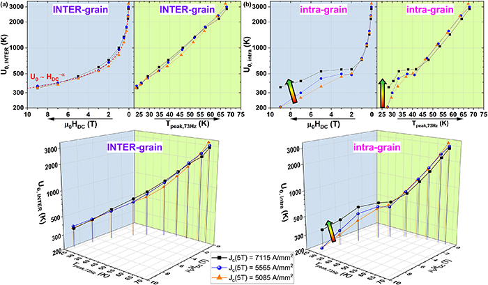
Figure 8. (a) INTER-grain and (b) inter-grain 3D plots with (on top) their respective 2D projections for the three Bi-2212 samples. The plots are showing U0 data as a function of DC field, µ0 HDC , and temperature of the 73 Hz peak, Tpeak,73Hz (data obtained with µ0 Hac = 1 mT). Note that the x-axis of the 2D U0 versus µ0 HDC projections is reversed to match the 3D plots. The red dashed line in the first panel is a power-law guide for the eye.
Download figure:
Standard image High-resolution image4. Discussion
In the following we divide the discussion in three main topics. Firstly, we take on deff, with its amplitude and field dependence, explaining the role played by the microstructure and the bridging level. Then, we compare the results obtained by the Kramer extrapolation and the irreversibility lines, providing a simple relation that allows the estimation of the low temperature HIrr, and we discuss the possible effect of the anisotropy on the overall performance. Finally, we compare the field and temperature dependence of the intra- and INTER-grain pinning energies, showing the important contribution of the former on achieving the highest Jc .
4.1. Effective filament diameter
The effective filament diameter deff significantly varies with changing Tmax, and so Jc . In particular, the smallest deff is achieved for the higher Jc wire, which also has the shortest time in the melt (because of the lowest Tmax). As demonstrated by Jiang et al the low Tmax generates the least interfilament bridging, almost keeping the original filament structure [8]. As shown in figure 2, in the best case deff(4.2 K) mildly decreases with increasing field (35%–37% of dBundle), whereas stronger changes are observed in the other two cases (55%–62% and 51%–59% of dBundle). A similar decreasing deff trend was previously found in a different type of Bi-2212 wires in [35], where the investigation was performed in a wider temperature range. The authors found a strong difference in deff depending on the wire quality and architectures (deff(10 K, 4–7 T) ∼70%–80% dBundle in the best case), but also observed a clear temperature dependence with deff approaching the filament size at higher temperature (>20–25 K) and increasing toward dBundle with decreasing temperature. Both our and their results demonstrate that deff has variations with field and temperature that have to be kept in mind for magnet design and protection.
The decrease of the field-dependence of deff with increasing Jc is obviously related to the difference in the α values obtained by magnetization and transport measurements (figure 3(a)). The larger magnetization αm with respect to the transport αt is, in general, ascribed to the different electric field, which in transport is chosen as a criterion (here 1 µV cm−1) whereas in magnetization is mostly induced by the magnetic field ramp rate (here estimated to be 3 or 4 orders of magnitude smaller). Since with increasing the magnetic field the n-value in the E∼ (J/Jc )n relation typically decreases, the magnetization Jc (or △M) is usually more strongly field dependent. This explanation is however not adequate for these Bi-2212 wires where the n-values estimated from the transport data is almost field independent (n∼ 26). In Bi-2212 we have to take into account the microstructural changes to understand the difference between αm and αt . Although Bi-2212 wires are microscopically isotropic, the filaments are locally bi-axially textured [17] but with an average c-axis orientation changing along the filaments, as schematically represented by the blue stripes in figure 3(b). These filaments can be connected by bridges, some of which have current carrying capability, and these bridges are more numerous in the high-Tmax, low-Jc wires (a bridge is represented in figure 3(b) by a magenta element). Since transport Jc is determined by the percolative path, α changes with the density of bridges. In fact, in the higher Jc wire with the least bridging, the current is forced to stay within the filaments for longer length with its current being more strongly limited by the filament worst orientation, which has the stronger field dependence (H//c-axis) inducing a large transport αt . In wires with more bridging (lower Jc ) the current can more likely bypass segments of the filaments with a less favourable orientation, percolating through bridges into better oriented filaments, as sketched in figure 3(b): this leads to a smaller transport α. The situation is more complex when α is evaluated by magnetization (αm ) because the total moment is determined by two current contributions: a long-range (sample-long) current, percolating through grain-boundaries and bridges, and local shorter-range inter- and intra-grain currents. The former, involving a global path across the entire sample, has likely a field dependence similar to that evaluated by transport measurements, so with a low α-value. On the other hand, the additional contributions by locally induced currents involve randomly oriented Bi-2212 grains, including grains with an high α-value, or short filament segments not involved in the global path because of their unfavourable orientation, so having an high α-value too. Since, in the lower-Jc wires, these unfavourably oriented (higher α-value) parts of the filaments are less involved in the long-range induced current (because of the many bridges that allow the global current to bypass them), they contribute more as local currents, with an increasing contribution to the total moment and so increasing the overall magnetization αm .
In our estimation of deff we did not take into account the deff dependence on the sample length as done in [16, 36] (our samples are very short, so approaching the zero-length limit). It is however interesting to follow their approach to estimate the connectivity transversal to the wire axis. In their case the effective filament diameter was exceeding dBundle and the equation  was used to estimate the 'fraction of longitudinal cross-sectional area of the strand which contains bridges' [16]. In our case deff is always smaller than the bundle size, so this equation does not apply. However, since we have no bundle-to-bundle bridging in these OPHTed wires, we can use a modified formula
  to instead determine the fraction of longitudinal cross-sectional area of the bundle which contains bridges, so an estimation of the intra-bundle connectivity. These values are reported in table 1 and reveal that in the higher-Jc
wire only 9% of the bundle area contains bridges, where for the lower-Jc
wires it increases to ∼16% (
to instead determine the fraction of longitudinal cross-sectional area of the bundle which contains bridges, so an estimation of the intra-bundle connectivity. These values are reported in table 1 and reveal that in the higher-Jc
wire only 9% of the bundle area contains bridges, where for the lower-Jc
wires it increases to ∼16% ( data at 5 T). Since
  is an intrinsic property (i.e. independent of the sample length), it allows a more direct sample-to-sample comparison than deff in case of significant length variation.
4.2. Kramer extrapolations, irreversibility lines and anisotropy
Figure 4 shows a good high-field rescaling for the Kramer plots. However, the HK values are obviously an underestimation of the real irreversibility fields. In this case HK was measured up to 45 K and the irreversibility curves were evaluated by AC susceptibility down to ∼25 K (figure 7), which allows us to compare the two datasets (at temperature ⩾ 35 K, a direct comparison of HIrr determined by the closures of the hysteresis loops and by AC susceptibility shows a good agreement; at lower temperature the high-field noise does not allow a reliable estimation of the loop closure). We found that in the 25–45 K range HK and HIrr are proportional with very close HIrr/HK ratio of ∼1.72–1.77 in these three samples. In figure 9 we replot the AC data and fits obtained in figure 7, including the low-temperature extension of the fits (dashed lines), and compare them with the HIrr data obtained by rescaling the VSM HK according to this HIrr/HK ratio. The agreement is reasonably good, giving an irreversibility field at 10 K of ∼60–70 T, which is certainly of interest for application of Bi-2212 in cryocooled machines.
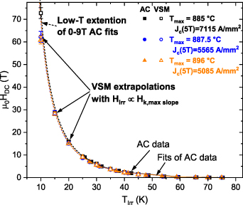
Figure 9. Extended irreversibility lines for the three wires. The solid symbols and solid lines are the AC susceptibility data for the INTER-grain contributions and their fits from figure 7. The dashed lines are the low-temperature extensions of the same fitting curves. The open symbols are the HIrr data obtained by multiplying HK for the HIrr/HK ratio as described in the text.
Download figure:
Standard image High-resolution imageOnly small differences are found in the AC-determined irreversibility lines in these samples, with a more obvious variation in the intra-grain lines, indicating that varying the OPHT causes more significant variation in the intra-grain properties. However, the small changes in the INTER-grain lines indicate an inverse correlation between Jc and the material anisotropy γ; this trend is also confirmed when including previously measured samples, where the irreversibility line of sample with the lowest Jc (4274 A mm−2) can be fitted with the largest γ. Since, because of the anisotropy, the c-axis transport Jc is much smaller than the ab-plane Jc , the Jc-γ anti-correlation suggests that lowering γ could facilitate current percolation along the c-axis [37, 38] necessary for grain-to-grain connectivity when obstacles (e.g. secondary phases) or excessive grain misorientations along the longitudinal wire direction are present (see the particular Bi-2212 grain structure in [17]).
4.3. Pinning energies
In the case of the pinning energies the most obvious sample-to-sample differences are observed in the intra-grain trend. In fact U0,intra does not follow the typical power-law field dependence once the DC field has exceeded ∼2 T and the temperature drops below 40–45 K. This enhanced pinning efficiency is likely due to point pinning likely caused by vacancies or atomic defects, a pinning mechanism commonly found at low temperature in HTS materials. Figure 10 compares the INTER- and intra-grain pinning energy for the higher-Jc wire. To better understand the meaning of these data we need to take into account that, unless the pinning mechanisms change, U0 should decrease with increasing temperature or field. Figure 10 shows that the INTER- and intra-grain pinning energies quite clearly diverge once a small field is applied. The data in the red circles are at the same low field (0.25 T) and almost identical temperature (∼58 K) but the INTER-grain U0 is about 20% large than the intra-grain, indicating that in this temperature/field range the INTER-grain pinning is stronger than the intra-grain. On the contrary, the data in the green circles are at the same high field (9 T) and have similar U0 values (∼345 K); however, the intra-grain Tpeak is 4.3 K higher, indicating that the intra-grain pinning has become stronger than the INTER-grain pinning at these low temperatures. This demonstrates a cross-over of intra-grain pinning with respect to the INTER-grain one. Similar plots (not shown) for the lower-Jc samples do not provide such a direct comparison between the two pinning energies (we can only evaluate a trend line over an actual U0(Tpeak,HDC ) surface), so we cannot clearly establish whether an INTER-grain/intra-grain U0 cross-over occurs. However, in the lower-Jc samples, differently from figure 10, there is no cross-over in the U0(HDC ) projection and in the U0(Tpeak) projection the intra-grain line does not approach the INTER-grain one as close as in the higher Jc case. This indicates that, despite some additional intra-grain pinning centres becoming effective at low temperature also in the lower-Jc samples, they are not as efficient as in the higher-Jc case. This could be caused by a reduced density of pins (e.g. produced by a different doping state) and/or a suppressed efficiency, for instance due to their slightly higher anisotropy (higher anisotropy reduces the vortex-defect interaction).

Figure 10. 3D plot with (on top) its 2D projections for the higher-Jc Bi-2212 wire comparing the INTER- and intra-grain pinning energies. Shown are U0 data as a function of µ0 HDC and Tpeak,73Hz (data obtained with µ0 Hac = 1 mT).
Download figure:
Standard image High-resolution image
An overall conclusion of these results is that there are relatively small variations in the INTER-grain properties of both the irreversibility line and the pinning energy, whereas greater changes are found in the intra-grain properties. In particular, the low-temperature intra-grain pinning appears to be a key factor, maybe driven by γ, in increasing the Jc performance. In fact, the highest Jc sample has a U0,intra at 9 T and ∼27–28 K about 70% higher than the other two samples.
5. Conclusions
In this paper, we investigated the superconducting properties of a series of Bi-2212 samples whose performance was varied by changing the maximum temperature of the over-pressure HT. This is the simplest parameter to change in order to vary the time in the melt of the Bi-2212 phase, and it has a strong effect on both the wire microstructure and its performance.
We found that the higher Jc sample has properties markedly different from the others. Despite all wires have some level of bridging that involves a significant portion of the filament bundle, the best performing wire has a lower deff of the order of 35%–37% of dBundle (compared to more than 50% in the lower Jc wires) with a weak field dependence caused by a more filament-constrained percolative path.
The INTER-grain properties (irreversibility line and pinning energy) are only weakly affected by the variation of the HT, as also demonstrated by the small change in the Kramer field at 20 K (table 1), but they reveal a sensible change in the material anisotropy with an anti-correlation between Jc and γ. This most likely affects the intra-grain properties as well as the grain-to-grain connectivity. In fact, because of the only partial Bi-2212 texturing, c-axis current must occur to allow a global current percolation, and a lower anisotropy enable a larger c-axis Jc and a better connectivity. The intra-grain irreversibility line (which is an average of all possible crystal orientations) is more dependent on the HT, but the most pronounced difference is in the intra-grain pinning energy at low temperature (<40–45 K) that in the best wire clearly cross-over the INTER-grain pinning energy, demonstrating a clear change of dominant pinning mechanism. The enhanced connectivity and stronger pinning, likely induced by a mild suppression of γ, appear to be keys to the large difference in transport Jc . Our results also indicate that the percolative path in Bi-2212 wire is complex and variable with small variation of the HT. This implies that achieving the best wire performance is challenging because of the narrow HT window. Despite the plateau Jc performance are already good for magnet applications (the peak Jc -value cannot be reached in magnets because of the spatial temperature inhomogeneity during the HT), there is an ongoing effort to understand how to generate the peak Jc -performance in a wider HT temperature range, more suitable for magnet realization. This paper suggests that for further optimization decreasing γ could be beneficial to improve HIrr and Jc . This might be obtainable by a fine tune of the powder chemistry, the doping level and/or the HT.
Acknowledgments
This work is funded by the US Department of Energy, Office of Science, and Office of High Energy Physics under Award Number DE-SC0010421 and performed under the purview of the US-Magnet Development Program. This work was performed at the National High Magnetic Field Laboratory, which is supported by National Science Foundation Cooperative Agreements NSF DMR-1644779 and DMR-2128556, and by the State of Florida.
Data availability statement
The data that support the findings of this study are available at the following website: https://osf.io/mvx8d/ [39].