

Abstract
We report the effect of nitrogen partial pressure on the growth of niobium-titanium nitride (NbTiN) thin films through reactive sputtering of the NbTi target in the presence of Ar and N2 atmosphere. The N2 partial pressure was varied from 5.8% to 15.15% with respect to the Ar flow available in the chamber. We measured a critical temperature (TC) as high as 15.77 K for an N2 partial pressure of 6.8% for a 50 nm film deposited on an MgO substrate. The epitaxial growth of the NbTiN films is evident from the observed (200) and (400) XRD peaks with respect to the substrate. The superconducting properties were analyzed with respect to the observed values of TC, ΔTC, temperature dependence of the upper critical field (BC2), coherence length (ξ), diffusion coefficient (D), and the thermally activated flux flow behavior following the Arrhenius equation. The TC variation observed for the entire spectrum of N2 partial pressure variation is ∼11%, with TC getting saturated towards the higher end of the N2 content. While the TC variation with respect to N2 content is non-linear, the variation of BC2(0), diffusion coefficient, and zero temperature coherence length ξ(0) show a linear dependence. While the BC2(0) values show an increasing trend, D and ξ(0) values show a decreasing trend with respect to the increase of N2 partial pressure. It is concluded that the optimum window of N2 partial pressure for the reactive sputtering of NbTiN using a target of Nb0.7Ti0.3 for the present experimental conditions, in terms of epitaxial growth and obtaining the highest TC is within the range of 5.8% to 8.51%.
Export citation and abstract BibTeX RIS
1. Introduction
Niobium-titanium nitride (NbTiN) is one of the robust superconducting (SC) systems among the conventional s-wave superconductors [1] for fundamental research and applied superconductor technologies. In the fundamental research, ultra-thin films of NbTiN with a thickness of the order of coherence length (ξ) and lower manifest interesting properties such as superconductor-to-insulator transition (SIT) [2], charge Berezinskii–Kosterlitz–Thouless transition [3], the SIT behavior with quantum phase slips in 1D nanowires [4], etc. On the technological side, NbTiN has a large-scale application in fields such as tunnel junction mixers [5], SC–insulating–SC junctions [6, 7], and SC hot-electron bolometers (owing to its higher energy gap) [8], among others. NbTiN is also a preferred candidate for coplanar waveguide SC resonators [9] and applications-like SC nanowire single-photon detectors (SNSPDs) [10–14]. NbTiN is a ternary alloy and is a complete homologous system wherein the ratio of Nb to Ti is flexible to any value from 0 to 1 (Nbx Tiy −x N). On the lower end of the alloy phase diagram, the end product is TiN, while at the higher end of the alloy phase diagram, NbN precipitates. The TC of NbTiN is ∼16 K [15] and is comparable to that of NbN, and has got a relatively large penetration depth (∼260 nm) [16]. Because of its large λ values, the system is a good candidate for studies related to fluctuations of SC properties in two- and one-dimensions. Strain free NbTiN thin films can be grown over the lattice-matched substrates by reactive magnetron sputtering [17, 18]. Owing to the unprecedented interest in NbTiN for SNSPD application with very high detection efficiency and other characteristics required for single photon detection, the system has been going through intense scrutiny from the device fabrication and integration point of view with respect to quantum-enabled technologies [19].
High-quality NbTiN films can be grown by many methods such as CVD [20], MBE [21], ALD [22], reactive sputtering techniques [23], etc. In the reactive sputtering technique (which is the most common one for thin film fabrication) one can start with co-sputtering using Nb and Ti targets and converting them to Nbx Tiy −x N with a desired Nb/Ti ratio suiting different applications under optimized sputtering conditions. Reactive sputtering can also be done using a fixed Nbx Tiy target and optimizing the sputtering conditions to get Nbx Tiy N [24]. In the latter case, though the Nb/Ti ratio in the final product is almost fixed, the ratio depends on the sputtering conditions. Optimization of the sputtering conditions is required to get the best SC properties. The SC properties of NbTiN also depend on the thickness of the film [25], carrier composition [23], growth temperature [15] sputtering power [26], and the substrate material [24]. The final stoichiometry of Nb and Ti in NbTiN also plays an important role in deciding the SC properties of the system [2, 20]. The TC of Nb1−x Tix depends on the ratio of Nb/Ti, and a maximum TC ∼17 K is reported for the Ti content of x = 0.34 [27, 28] which is close to the bulk TC of 18 K. TC also depends on the substrate [29] and substrate temperature used for deposition. Yu et al [15, 30] have obtained a TC of 16.2 K for NbTiN on SiO2, wherein the substrate was kept at 450 °C. In comparison, the room temperature (RT) deposition yielded a TC of ∼11 K only. Similarly, deposition at 600 °C on copper cavity by Di Leo et al [31] have shown a TC of 17 K, which is very close to the bulk TC value, here the Ti content is 0.45 compared to the report by Yu et al. There are also reports, wherein TC of ∼15 K has been reported for NbTiN film of thickness ∼150 nm or higher and with N2 partial pressure in the range of ∼20% or higher [11, 24]. For SNSPD applications, devices are to be fabricated from SC films of thickness in the 2D regime, which for NbTiN films falls in the range of 10–20 nm. Moreover, NbTiN is one of the most studied systems for SNSPD applications as its performance indicators with respect to detection efficiency and jitter time are comparable or better than other systems such as MoSi, WSi, NbN etc [19, 32]. The present study is conducted to optimize the SC properties of NbTiN thin films towards the development of SNSPDs and to complement the existing literature on the deposition conditions and subsequent formation of NbTiN, specifically with respect to the role of N2 content (nitrogen partial pressure) in the chamber to transform Nb0.7Ti0.3 to Nbx Tiy N to get the best SC properties. The depositions were performed by maintaining a substrate temperature of 600 °C during the deposition to promote epitaxial growth and crystalline nature of the films. Nevertheless, a comparison has been done with RT deposited samples for the SC and the structural properties of the thin films including the chemical content evaluation by XPS analysis. For comparison with RT deposition, we have chosen the samples towards the lower end of the N2 partial pressure. The evaluation of the structural and SC properties was carried out by high-resolution x-ray diffraction (HRXRD) and XPS analysis and electrical transport measurements using Physical Property Measurement System (PPMS). We report a TC as high as 15.77 K for the films deposited with an optimal N2 partial pressure of 6.8% using MgO as the substrate. XPS analysis shows the availability of Ti ions for the RT deposited samples which hints at the incomplete reaction kinetics of conversion of NbTi to NbTiN at RT deposition. An analysis of the magneto-transport behavior with respect to thermally activated flux flow (TAFF) models from the onset of SC transition to the zero-resistance state is carried out to understand the role of magnetic field on the transition region and its suitability towards SNSPD applications.
2. Experimental
NbTiN thin films were grown on MgO (001) single-crystal substrates by reactive DC magnetron sputtering with a base pressure of ∼2 × 10⁻⁷ mbar. The depositions were performed at a temperature of 600 °C to ensure crystallinity and phase conversion from NbTi to NbTiN. We used Nb0.7Ti0.3 target to grow Nbx Tiy N thin films. The phase conversion from Nb0.7Ti0.3 to Nbx Tiy N was aided with the help of controlled flow of nitrogen and argon into the chamber using calibrated mass flow controllers. Before deposition, substrates were annealed at ∼750 °C to get rid of contaminants. Sputtering was performed at a DC power of 80 W, for different nitrogen partial pressures such as 5.8% (S1), 6.8% (S2), 8.5% (S3), 12.5% (S4), 13.51% (S5), and 15.15% (S6) which were maintained by flowing a mixture of N2 and Ar gas into the chamber. As there are reports on the deposition of NbTiN through DC magnetron sputtering at RT [12, 24] for our own reference and for comparative studies, we also have performed RT deposition of NbTiN films by selecting two conditions on the lower end of the N2 concentration (i.e. for the conditions of S1 and S2). Films were grown with a thickness of 50 nm which was controlled by deposition time and rate and was further confirmed with a thickness profiler (Model—NanoMap-500LS). Structural characterization and the transport properties of the films were studied using HRXRD (X' Pert PRO PANalytical) and PPMS (Cryogenic), respectively. XPS studies were used to determine the chemical composition of the films and for the estimation of residual oxygen content due to native oxidation or that may remain due to oxidation of unreacted species remaining due to partial reaction during deposition. The SC properties of the samples were evaluated by measuring resistance as a function of temperature and magnetic field up to 5 T. RT hall measurements were performed for all the samples to estimate the carrier density, Hall coefficient, density of states, and Fermi velocity etc. A detailed description of the samples, preparation conditions, and their SC properties and physical parameters obtained from the Hall measurements are given in table 1.
Table 1. The physical parameters obtained from room temperature Hall measurements and superconducting properties of NbTiN thin films prepared with varying N2 partial pressure during sputter deposition.
| Sample | N2 partial pressure (N2/(Ar + N2)) (%) | Resistivity 
| Carrier density 
| Hall coefficient 
|
KF

|
VF

|

|
D
 (From Hall measurements) (From Hall measurements) |
N (0) 
| TC (K) | ΔT (K) |
D
 (from low temperature transport data) (from low temperature transport data) |
 (0) nm (0) nm |
 (K) (K) |
|---|---|---|---|---|---|---|---|---|---|---|---|---|---|---|
| S1 | 5.88 | 4.153 | 8.67 | 7.20 | 1.36 | 1.58 | 2.50 | 13.2 | 1.13 | 15.26 | 0.18 | 9.1 | 4.22 | 571.25 |
| S2 | 6.67 | 3.379 | 11.62 | 5.36 | 1.51 | 1.75 | 2.53 | 14.8 | 1.25 | 15.77 | 0.14 | 9.0 | 4.12 | 571.03 |
| S3 | 8.51 | 5.227 | 8.21 | 7.59 | 1.34 | 1.55 | 2.06 | 10.7 | 1.11 | 15.01 | 0.09 | 7.4 | 3.83 | 572.21 |
| S4 | 12.5 | 7.915 | 6.92 | 9.01 | 1.27 | 1.47 | 1.52 | 7.48 | 1.05 | 14.10 | 0.35 | 6.4 | 3.67 | 572.57 |
| S5 | 13.51 | 7.693 | 5.76 | 10.82 | 1.19 | 1.38 | 1.77 | 8.19 | 0.99 | 13.97 | 0.38 | 6.6 | 3.69 | 572.83 |
| S6 | 15.15 | 7.848 | 5.52 | 11.31 | 1.17 | 1.36 | 1.79 | 8.14 | 0.97 | 13.95 | 0.32 | 6.1 | 3.61 | 572.84 |
| S1 RT | 5.88 | 14.510 | 7.17 | 8.71 | 1.28 | 1.48 | 0.81 | 4.03 | 1.06 | 10.8 | 0.13 | |||
| S2 RT | 6.67 | 17.642 | 6.83 | 9.13 | 1.26 | 1.46 | 0.69 | 3.37 | 1.04 | 10.5 | 0.18 |
3. Results and discussion
Figure 1 shows the HRXRD pattern of all the samples (samples deposited at RT and at 600 °C along with the deposition conditions) for the 2θ range from 30° to 100°. Epitaxial growth NbxTiyN is evident for the samples deposited at 600 °C, which is confirmed with the observed diffraction peaks of the oriented planes with respect to the substrate such as (200) and (400). It is also noteworthy that the respective positions of the (200) and (400) peaks shift towards lower angles except for the sample S2 (for which the peak position is shifted relatively towards the higher angles) indicating an induced strain (residual stress) with respect to the N2 variation. In comparison, the RT deposited samples do not show any peaks of NbxTiyN or any other phases such as NbN, TiN or NbTi etc. This shows that the nitridation process of NbTi to NbTiN is not effective for the RT deposited samples, the deposited film remains as mostly amorphous; wherein the diffraction peaks corresponding to the substrate only appear. The lattice constants of the samples with respect to N2 variation were calculated assuming a cubic δ-(Nb, Ti)N (Fm3m) phase (following the JCPDS file 04-002-7196 for the NbTiN) [20] which are plotted in figure 2 along with other sample parameters such as TC, BC2(0), and relative intensities of the (200) and (400) peaks representative of induced texture (epitaxial growth of the sample). The variation of the lattice constant with respect to N2 content is nonlinear. While the sample S2 shows the smallest lattice constant which is in agreement with the literature [23], as the N2 content increases, the lattice constant also increases gradually and gets saturated towards higher N2 content. The sample S1, which has a lesser nitrogen content also has a lattice constant higher than that of the S2. Reported studies indicate the possibility of forming hexagonal and cubic phases of NbTiN [20], depending on the deposition temperature and N2 content. For the present study, the XRD data closely matches with the cubic phase. Further analysis such as HRTEM, in-plane XRD scans etc are required to confirm the co-existence of cubic and hexagonal phases, which is beyond the scope of the current article. Though there are several phases of NbTiN, the cubic phase with rock salt crystal structure is reported to have a higher TC of ∼16 K [23]. The XRD intensity ratio of (200) and (400) peaks are the highest for the S2 condition and decreases as the N2 content increases in the chamber. S1 also shows a lower intensity compared to S2. This indicates that the S2 condition is more favorable for the epitaxial growth of NbTiN phase with respect to the present deposition conditions and the target stoichiometry. As we could not observe peaks corresponding to other diffraction planes as well as for other phases, it should be concluded that the reaction kinetics of the growth of NbTiN from Nb0.7Ti0.3 target with respect to the present sputtering conditions and the target bias are at the optimal level. A N2 partial pressure within the range 5.8%–8.51% is best suited for obtaining epitaxial growth of the films.
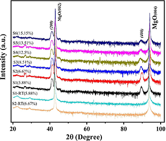
Figure 1. HRXRD spectrum of the samples. The relative peak intensities of the aligned peaks of (200) and (400) are varying with respect to the N2 content during deposition, with the condition S2 giving a maximum peak intensity for both of the planes. A closer examination of the peaks also reveals that the full width at half maximum (FWHM) of these peaks also varies in the similar fashion as that of the peak intensities, with the least FWHM for the S1 sample (0.94°), and the FWHM gradually increases with respect to the N2 content and reaching the value of 1.21° for the sample S6. For the sample S4, an unidentified peak was observed near to 2θ of 67°.
Download figure:
Standard image High-resolution image
Figure 2. Variation of TC, BC2(0) (lower panel), lattice constant, and relative intensities of the (200) and (400) XRD peaks (upper pane) with respect to the nitrogen partial pressure. It is seen that TC variation follows the variation of the relative peak intensities of the XRD peaks.
Download figure:
Standard image High-resolution imageThe chemical composition and the estimation of the oxygen content on the films were done through XPS measurements with a PHI 5000 Versa Probe III XPS utilizing Al (Kα) radiation of energy = 1486 eV. The result of XPS measurements in the form of a percentage ratio of the individual ions present in the films as well as the chemical species detected through fitting process are given in table 2. The ratio of Nb:Ti for all the samples is ∼70:30 which is roughly equal to the target stoichiometry used. The fitting of the XPS peaks showed the presence of NbN, TiN, TiN0.9, NbO, and Nb2O5 in all the samples, whereas as TiO2 appears for RT deposited samples. It is well known that both Nb and Ti are prone to oxidation on exposure to ambient atmosphere. Oxide forms such as NbO, NbO2, and Nb2O5 etc are the results of native oxidation of Nb films, which act as a protective layer preventing further oxidation [33–37]. XPS studies on NbTiN thin films [38] showed the presence of native oxides such as Nb2O5 and TiO2 which are due to the surface oxidation of Nb and Ti respectively. In the present case, the presence of NbO and Nb2O5 in all the samples can be considered as the result of native oxidation process on the surface of the films, whereas the presence of TiO2 in the RT deposited samples hints at the availability Ti ions in these samples to form TiO2 on contact ambient conditions. From table 2, it can be understood that the O2 content reduces with respect to the increase of N2 partial pressure as well as for deposition at elevated temperature. The XPS spectra recorded along with the fitting and deconvolution of the spectra to identify the individual chemical species is given as figure S1 in supplementary document.
Table 2. Results of XPS measurements showing elemental analysis and the chemical species detected. Note that the oxygen content for room temperature deposited samples are much higher than that of the samples deposited at 600 °C.
| Sample | Chemical species identified through fitting of the XPS spectra | Nb 3d (at %) | Ti 2p (at %) | N 1s (at %) | O 1s (at %) | Ratio of Nb:Ti |
|---|---|---|---|---|---|---|
| S1 RT | NbN, TiN, TiN0.9, NbO, Nb2O5, TiO2 | 25.27 | 10.02 | 24.40 | 40.32 | 71.60:28.40 |
| S2 RT | NbN, TiN, TiN0.9, NbO, Nb2O5, TiO2 | 25.29 | 10.35 | 29.64 | 34.73 | 70.96:29.04 |
| S1 | NbN, TiN, TiN0.9, NbO, Nb2O5 | 27.85 | 11.21 | 31.89 | 29.05 | 71.30:28.70 |
| S2 | NbN, TiN, TiN0.9, NbO, Nb2O5 | 33.37 | 13.47 | 34.81 | 18.35 | 71.24:28.76 |
The measurements of SC transport properties of the films were carried out using PPMS down to a temperature of 2 K and with a magnetic field of upto 5 T. We have performed resistance measurements as a function of temperature for different magnetic fields [RT(B)]. Figure 3 shows the variation of resistance as a function of temperature from 20 K down to 12 K for an applied magnetic field of 0 T, wherein the SC transition of the samples is clearly registered. TC of the thin films was defined as the temperature at which the resistance of the film drops to 50% of the value at 20 K (R20 K). A TC as high as 15.77 K has been observed for sample S2. The overall variation of TC for the whole variation of N2 content in the chamber is ∼11% (15.77 K for S2 and 13.95 K for S6) when the N2 content is varied from 5.8% to 15.15%. The RT deposited samples show a much lesser TC (11 K, for S1RT, and 10.6 K for S2RT samples), a TC enhancement of ∼30% is visible with respect to the high temperature deposition. The observed TC for RT deposited samples is in agreement with that reported by Jia et al [13], wherein a TC of ∼10 K has been observed for NbTiN samples deposited on Si and SiOx -Si substrates, but the N2 partial pressure used by them is ∼16.66%, which is higher than what we have used in the present study. In a similar report, Yu et al [15] have found that deposition at higher temperature will enhance the TC from about 12 K (for RT deposited samples) to ∼16 K (for samples deposited at 450 °C) compared to the samples deposited at RT. In both the above studies the N2 partial pressure used for deposition is ∼20%, which is much higher than the range used in the present study. In a similar study, by Makise et al [24] have reported a TC ∼ 15 K for RT deposition on substrates such as MgO, Al2O3 and fused quartz, wherein they have reported crystalline growth for films of thickness in the range ∼150–300 nm. Here again the N2 partial pressure under investigation is from ∼20% and above. In contrast, [24] reports a linear dependence of lattice constant with respect to an increase in the partial pressure of N2 with respect to all the substrates involved, whereas in the present case the optimum condition shows lower lattice constant compared to the rest of the conditions. Compared to the earlier reports on the RT depositions of NbTiN [11, 13, 24], we obtained amorphous films for deposition at RT, this presumably could be due to the lower thickness (50 nm) of the films opted for the current study. From figure 3, it can be seen that the TC of the NbTiN thin films increases initially with respect to N2 content upto S2, and then decreases thereafter. One can see that the variation of TC follows the same trend as that of the variation of XRD peak intensities of the oriented planes [(200) and (400)]. ΔTC of the samples (ΔTC = TC-90−TC-10), wherein TC-90 and TC-10 are the temperatures at which the resistance drops to 90% and 10% of the normal state resistance (R20 K) were also estimated from the R–T plots. ΔTC is an estimation of the quality of the SC state, with lower ΔTC associated with a better quality of superconductivity. The values of ΔTC are given in table 1. Samples show a relatively wider transition from the sample condition of S4 onwards, as the ΔTC values are higher, while the samples S1 to S3 show relatively lesser ΔTC values, with S3 having the least ΔTC. In the inset of figure 3 is shown the normal state resistivity variation of all the samples. Resistivity is lowest for the S2 condition, while the RT deposited samples show much higher resistivity values. The other physical parameters related to the samples obtained from RT Hall measurements and the results obtained from low temperature transport measurements are given in table 1. From table 1, we can see that the carrier density, diffusion coefficient, and mean free path are higher for sample S2. In corroboration with XRD analysis, this indicates that the crystallinity of this sample is better than the rest of the conditions. It is to be noted that RT diffusion coefficients obtained from the RT Hall measurements and that obtained from the SC transport measurements at low temperature are roughly agreeing to each other with slightly elevated values obtained from RT measurements.
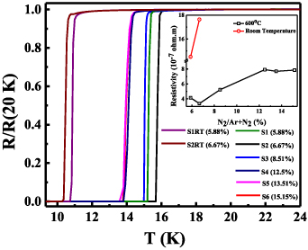
Figure 3. Resistance as a function of temperature for the films grown at different Nitrogen content. The highest TC is observed for S2 sample with 6.8% of N2 content. Above 6.8% of N2 content, the TC decreases continuously and saturates towards the N2 content of 13% and more.
Download figure:
Standard image High-resolution imageFigure 4 shows the resistance variation as a function of temperature for different magnetic fields [RT(B)] of the samples in the temperature range 20 K–8 K, with an applied magnetic field of upto 5 T. The RT(B) curves are shown for selected three samples viz. S1 (figure 4(a)), S2 (figure 4(b)), and S4 (figure 4(c)). As expected, as the magnetic field is increased the TC of the samples decreases. From the RT(B) data, BC2(T) values were determined as a function of temperature, and the results are plotted in figure 4(d). We estimated the Ginzburg–Landau coherence length [ξ(0)] for all the samples using the expression,
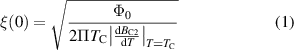

Figure 4. RT(B) of the representative samples S1, S2, and S4 along with the variation of the measured value of BC2 as a function of temperature.
Download figure:
Standard image High-resolution imagewhere dBC/dT is the slope of the BC2 versus T(T = TC) curve, Φ° (=h/2e) is the SC flux quantum. The BC2(0) of all the samples were estimated by extrapolating the temperature-dependent BC2 to the zero-temperature value. Alternatively one can use the formula BC2(0) = Φ°/2Πξ(0)2 [39]. In figure 4(d) the solid lines are linear fit related to the Ginzburg–Landau theory [40, 41] for the temperature dependence of the upper critical field of superconductors. We also have calculated the electronic diffusion coefficient using the expression
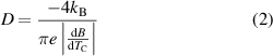
where kB is the Boltzmann constant and e is the electronic charge [42].
The SC parameters deduced such as TC, ΔTC, dB/dT, BC2(0), D, and ξ(0) for all samples are listed in table 1. It is evident from table 1 that the SC properties of the prepared films are dependent on N2 partial pressure available in the chamber. Samples S1, S2, and S3 which are at the lower end of N2 partial pressure show relatively higher TC and lesser ΔTC, which implies that this window is more favorable for obtaining better SC properties of the films. Samples S4 to S6 have relatively lesser TC values with broad SC transitions and higher BC2 values. This hints that these conditions are favorable for growing films for technological applications which require high magnetic fields and current densities.
We also analyzed the broadening of the SC transition between the TC-ON and TC-zero using the TAFF model [43]. TAFF follows the Arrhenius law,
where Uo is the activation energy of vortices, Ro is the pre-exponential factor, and kB is the Boltzmann constant. Uo can be extracted from the slope of ln(R) vs 1/T curves, and the values obtained as a function of applied magnetic field are shown in figure 5 for all the samples. In the inset of figure 5 is the corresponding Arrhenius plots of the sample S2 at different magnetic fields from where the activation energies have been estimated. It is to be noted that all the red lines in the inset of figure 5 merges to a common crossover point (Tcr) which is ∼15.5 K, and nearly matches with the TC of this sample. TAFF behavior is dominated by the flow of flux vortex and is directly related to the flux pinning mechanisms available within the sample. The flux pinning mechanisms depend on many factors such as phase purity, defects including grain boundaries, and even the texturing of the samples (epitaxial growth of the film). In the present case there are no secondary phases present as is evident from the HRXRD analysis, but with respect to the N2 content, the induced strain in the sample changes and also the texturing of the grains which can directly affect the TAFF behavior of the samples. So, as we evaluate the behavior of different samples using the TAFF, it is difficult to emphasize which of the above factors dominate for the apparent activation of flux Abrikosov vortices with respect to the magnetic field. This is evident from figure 5 that samples S2 and S6 are showing relatively higher activation energies in overall comparison to the other samples, while the activation energy of sample S5 is lower in comparison. The dependence of the activation energies of the other samples with respect to magnetic fields are more or less the same, which means, presumably the difference between these samples for the flow of flux Abrikosov vortices with an applied magnetic field is apparently nil. It should be noted that sample S2 shows the best TC, while the TC of S5 and S6 are almost the same, wherein the TAFF behavior of the S2 and S6 closely matches with U0 values of the sample S6 are slightly higher compared to S2. Though TAFF behavior shows dependence on the N2 content during deposition, a systematic study to understand its dependence on the individual parameters such as the quality of the films, texturing, defects, and other flux pinning mechanisms would be of interest for further analysis.

Figure 5. The variation of activation energies of the samples with respect to magnetic field, calculated following the Arrhenius model of the thermally activated flux flow (TAFF) of vortices. Inset shows the Arrhenius curve for the S6 sample in the presence of magnetic field.
Download figure:
Standard image High-resolution image
Similarly, the TC of a strong S-wave superconductor is governed by McMillan's equations [44]
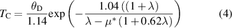
where θD is the Debye temperature, λ is the effective electron–phonon coupling constant, and μ* is related to the Coulomb pseudo potential. The TC analysis of our samples were done following a similar analysis done by Hazra et al [41]. The effective electron–phonon coupling constant λ is given by λ = N(0)U, where U is the attractive potential and N(0) is the density of states at the Fermi level. The Debye temperature θD is given by  , here Da is the atomic density, Y is Young's modulus and ρ is the mass density. In the present case, the lattice constant varies with respect to the N2 content, so θD also has direct dependence on the lattice constant. The calculated values of θD for all the samples are also shown in table 1 along with other sample specific parameters. Here we have taken the values of Young's modulus from the work of Arockiasamy et al [45] for the typical Nb/Ti ratio of Nb0.75Ti0.25. The variation in θD follows the variation of lattice constant, but the lattice constant is lowest for S2, while the TC is highest for this sample. This indicates that other factors such as electron–phonon coupling constant and Coulomb pseudo potential are also to be taken into account for concluding the observed TC variation. Nevertheless, in the present case, it should be noted that the extent of crystallinity/epitaxial growth is more dominant for the observed TC variation compared to the intrinsic parameters which we described above. The phase conversion from Nb0.7Ti.03 to Nbx
Tiy
N is aided with the incorporation of N2 in the sputtering chamber and a N2 partial pressure window of 5.8%–8.5% is better with respect to the epitaxial growth and SC properties of the final product.
, here Da is the atomic density, Y is Young's modulus and ρ is the mass density. In the present case, the lattice constant varies with respect to the N2 content, so θD also has direct dependence on the lattice constant. The calculated values of θD for all the samples are also shown in table 1 along with other sample specific parameters. Here we have taken the values of Young's modulus from the work of Arockiasamy et al [45] for the typical Nb/Ti ratio of Nb0.75Ti0.25. The variation in θD follows the variation of lattice constant, but the lattice constant is lowest for S2, while the TC is highest for this sample. This indicates that other factors such as electron–phonon coupling constant and Coulomb pseudo potential are also to be taken into account for concluding the observed TC variation. Nevertheless, in the present case, it should be noted that the extent of crystallinity/epitaxial growth is more dominant for the observed TC variation compared to the intrinsic parameters which we described above. The phase conversion from Nb0.7Ti.03 to Nbx
Tiy
N is aided with the incorporation of N2 in the sputtering chamber and a N2 partial pressure window of 5.8%–8.5% is better with respect to the epitaxial growth and SC properties of the final product.
4. Conclusion
The optimization of the SC properties of NbTiN thin films with respect to the N2 partial pressure during the sputter deposition of Nb0.7Ti0.3 has been studied. The N2 partial pressure varied from 5.8% to 15.15% with respect to the Ar flow into the chamber. A TC as high as 15.77 K has been observed (for a film of thickness 50 nm deposited on MgO substrate) for a N2 partial pressure of 6.8% with respect to the Ar flow. The films show a signature of strain with respect to the N2 content, wherein the lattice constant is minimum for the samples having 6.8% of N2 content, while for other samples lattice constant shows an increasing trend with respect to the N2 content. In comparison, the RT deposited samples have shown no signature of crystallinity of the phase formation of NbTiN, and the TC measured for the RT deposited samples are much lower than that of the samples deposited at 600 °C. XPS analysis showed the presence of TiO2 in RT deposited samples showing the availability of Ti ions hinting at the incomplete conversion of NbTi to NbTiN for RT deposition. We analyzed the variation of resistance in the presence of magnetic field using the TAFF model and calculated the activation energy by Arrhenius law. The flux flow mechanism in type-II superconductors exhibits complex behavior with respect to the different pinning mechanisms available. So, a conclusive picture of the variation of activation energy calculated from Arrhenius law is difficult to obtain. It is to be noted that with respect to current target stoichiometry, and other sputtering conditions for the reactive sputtering of NbTiN, N2 partial pressure within the window of 5.8%–8.51% is found to be optimum with respect to the SC properties of the film. The findings of this study are very relevant for any attempts to fabricate 2D films and meander structures for single photon detection applications.
Acknowledgments
Pratiksha Pratap would like to acknowledge UGC, India for the research fellowship and AcSIR, India for PhD registration. Financial support is acknowledged from DST through the QuEST(Q-65) project and from CSIR through the FCP project. Authors acknowledge Dr Manju Singh and Dr Rajib Rakshit for initiating this work at CSIR-NPL. They thankfully acknowledge Professor Ramesh Chandra from IIT-Roorkee for providing the XPS facility.
Data availability statement
All data that support the findings of this study are included within the article (and any supplementary files).
Supplementary data (0.3 MB PDF)