

Abstract
The progressive miniaturization of superconducting quantum interference devices (SQUIDs) used, e.g. for magnetic imaging on the nanoscale or for the detection of the magnetic states of individual magnetic nanoparticles causes increasing problems in realizing a proper flux-bias scheme for reading out the device. To overcome the problem, a multi-terminal, multi-junction layout has been proposed and realized recently for the SQUID-on-tip configuration, which uses constriction-type Josephson junctions (JJ). This geometry is also interesting for SQUIDs based on overdamped superconductor—normal metal—superconductor (SNS) JJ. We fabricated four-terminal, four-junction SQUIDs based on a trilayer Nb/HfTi/Nb process and study their static and dynamic transport properties in close comparison with numerical simulations based on the resistively and capacitively shunted junction model. Simulations and measurements are in very good agreement. However, there are large differences to the transport properties of conventional two-junction SQUIDs, including unusual phase-locked and chaotic dynamic states which we describe in detail. We further extract the current-phase relation of our SNS junctions, which turns out to be purely sinusoidal within the experimental error bars.
Export citation and abstract BibTeX RIS

Original content from this work may be used under the terms of the Creative Commons Attribution 4.0 license. Any further distribution of this work must maintain attribution to the author(s) and the title of the work, journal citation and DOI.
1. Introduction
Miniaturized superconducting quantum interference devices (SQUIDs) offer high spatial resolution and high sensitivity for the detection and investigation of magnetic sources on the nanoscale. To achieve high spin sensitivities, even below 1 µB/Hz1/2 (µB is the Bohr magneton) [1], and to improve their coupling, e.g. to individual magnetic nanoparticles (MNPs), nanowires or nanotubes [2–10], it is crucial to downscale the linewidth of the SQUID loop [11–13] and the size of the Josephson junctions (JJs) intersecting the loop. Therefore, direct current (dc) SQUIDs with lateral size in the µm range (microSQUIDs) or even sub-µm range (nanoSQUIDs) have received increasing attention during the last years [14, 15] and already have promising applications for high-resolution scanning SQUID microscopy [1, 16–25]. Additionally, downscaling the dimension of the SQUIDs makes them insensitive to strong external magnetic fields [26, 27].
On the other hand, downscaling makes it increasingly difficult to modulate the magnetic flux through the SQUID using flux-modulation lines. An elegant solution has been presented in [28, 29], where the traditional two-junction SQUID-on-tip (SOT) [1] was replaced by a multi-terminal SOT configuration containing three or four junctions in the SQUID loop. Biasing the individual junctions allows adjusting the SQUID to optimal sensitivity for all values of an applied magnetic field. The SOT contains constriction-type JJs where self-heating leads to current voltage characteristics (IVCs) which are hysteretic under current bias and thus require a voltage bias to operate the device slightly above its critical current. Consequently, the analysis in [28] focused on the static behaviour and the critical current of the multi-terminal SOT.
The use of SNS-type JJs, where N indicates the normal conducting barrier of the junction and S denotes the superconducting electrodes, can allow for non-hysteretic IVCs of the individual junctions and consequently for a more traditional readout where the SQUID is current-biased in the resistive state. However, having in mind highly miniaturized SQUIDs, the problem of an adequate flux modulation remains and, thus, the concept of the multi-junction SQUID is also very attractive for SQUIDs based on SNS junctions. In contrast to asymmetric two-junction SQUIDs, where the asymmetry of the junctions or the SQUID loop and therefore the shift of the quantum interference pattern is chosen with the design, the multi-junction SQUIDs offer the possibility to shift the pattern continuously. Thus, the optimal working point can be adjusted precisely and independently of the parameter spread during the fabrication. Furthermore, the multi-terminal, multi-junction SQUIDs are superior to two-junction SQUIDs with direct injection feedback current to adjust the flux bias, since they offer two additional control currents, enhancing the electric tunability of the SQUIDs. This makes them more suitable for noise reduction schemes, which are based on periodic flux-bias switching of the SQUIDs [28, 30].
The dynamics of a conventional two-junction SQUID is understood very well on the basis of the resistively and capacitively shunted junction (RCSJ) model [31, 32]. Such an approach is also very reasonable for a multi-junction SQUID. However, one may expect nontrivial interactions of the four junctions and consequently a behaviour which may strongly deviate from a traditional device. This expectation motivates our theoretical and experimental study of the dynamics of SNS-type multi-junction SQUIDs, using a configuration with four junctions embedded in the SQUID loop. Connecting to [28] we first analyze the critical current of the device as a function of various control parameters. We then turn to the resistive state and study IVCs and voltage vs. flux modulation patterns, with the finding of several unusual dynamic states.
The organization of the paper and the main results are as follows. In section 2 we first introduce the mathematical model and subsequently use it to analyze the dynamics of a 4-JJ SQUID with (nearly) symmetric junctions. In the resistive state we find a complex interplay between phase-locked and chaotic states, leading, e.g. to an unusual hysteresis in the SQUID IVC and to multiple-valued voltage vs. flux modulation patterns. Section 3 focuses on the experimental device and contains a comparison of its transport characteristics to simulations. The section starts with some details on the fabrication and the design of the device (section 3.1) and then turns to a basic characterization in terms of critical current vs. flux patterns, IVCs and voltage vs. flux modulation patterns (section 3.2). The comparison between experiment and simulation shows that one of the junctions of the experimental device is in essence shorted (i.e. the junction has a very high critical current) so that effectively we have an asymmetric 3-JJ SQUID. Taking the actual device parameters into account we find excellent agreement between measurement and simulation. Section 3.3 focuses in more detail on the behaviour our device when one of the junctions is biased by an additional current. Here, a peculiar state is detected, where the junctions in one of the SQUID arms are in the resistive state, but with opposite dc voltages, while the junctions in the other arm of the SQUID remain in the zero-voltage state. Section 3.4 is devoted to the determination of the current-phase relation (CPR) of two of the JJs. The CPR's are extracted from the data by using a procedure introduced in [28] and turn out to be purely sinusoidal within the experimental error bars. Section 4 concludes our work.
2. Numerical simulations
2.1. Mathematical model
We consider the 4JJSQ as schematically depicted in figure 1, with four ports (p = 1,..., 4). Three independent currents I1, I2 and I4 can be injected via ports 1, 2 and 4, respectively. The current I3 to port 3 is used as a drain, i.e. we have I3 = I1 + I2 + I4. Each loop segment between neighboring ports contains one JJ; i.e. the SQUID loop is intersected by four JJs (k = 1,...,4). We consider I1 as a bias current and I2 and I4 as control currents, and we will discuss how the critical current Ic1 (from port 1 to 3) and the voltage VSQ (between port 1 and 3) will change with the control currents and with Φext.

Figure 1. Schematic layout of the 4-terminal SQUID (with ports p = 1–4) intersected by 4 Josephson junctions (k = 1–4) with phase differences δk . The bias current I1, the drain current I3 and the control currents I2 and I4 as well as the currents Jk through the kth junction are indicated by arrows. The inductances of the loop segments between the four ports are denoted by Lk.
Download figure:
Standard image High-resolution imageThe Josephson current through the kth junction is IJ,k = I0 ak sin(δk ), with asymmetry parameters ak and gauge-invariant phase differences δk of the superconducting wave functions across the kth JJ. Here, we define I0 as the average (I0,left-min + I0,right-min)/2 of the (noise-free) critical currents of those two JJs which have the lower critical current in the left and right SQUID arm, respectively. Accordingly, the sum of the asymmetry parameters of those two 'weakest JJs per SQUID arm' is 2. This choice for the definition of I0 ensures that the (noise-free) critical current Ic1 vs. Φext for I2 = I4 = 0 of the 4JJSQ has a maximum Ic1,max = 2I0.
Normalizing currents to I0, we obtain in normalized form for the Josephson currents iJ,k = ak sin(δk ). To capture also dynamic properties of the 4JJSQs, we describe each junction within the resistively and capacitively shunted junction (RCSJ) model [31–33], i.e. we also consider quasiparticle currents through the junction resistance R, and displacement currents across the junction capacitance C. For simplicity, we assume that R and C are the same for all four JJs. The SQUID loop shall have a total inductance L = Σk=1 4 Lk , where Lk denote the inductances of the loop segments between the four ports (see figure 1).
In normalized form the RCSJ equations read:


Here, βC = 2πI0 R2 C/Φ0 is the Stewart-McCumber parameter with the magnetic flux quantum Φ0 = h/2e ≈ 2.0678 · 10−15 Vs. In equation (1) time is normalized to Φ0/(2πI0 R) and currents are normalized to I0. ∂t indicates derivatives with respect to the normalized time. The currents iN,k denote normalized noise currents with (normalized) spectral density 4Γ, where Γ = 2πkB T/(I0Φ0) is the noise parameter.
The normalized currents jk can be found from the conditions i1 = j1 − j4, i2 = j2 − j1, i3 = i1 + i2 + i4 = j2 − j3 and i4 = j4 − j3. With the definition of an average circulating current jSQUID = Σk =14 jk /4 one obtains:


Using (in dimensioned units) Σk =1 4 LkJk + Φext = (Φ0/2π) [δ3 + δ4 − δ1 − δ2], the current jSQUID can be related to the phase differences δk via:

with the screening parameter βL = 2I0 L/Φ0. Here, ϕext is the magnetic flux (normalized to Φ0) applied to the SQUID loop and ϕb is the normalized flux due to additional fluxes generated by the normalized bias current i1 and control currents i2 and i4 in the case of asymmetric inductances,
where lk = Lk /L.
We solve the equation (1) using a 5th order Runge Kutta method, together with equations (2 a)–(4). The time derivatives ∂t δk equal the normalized voltages uk = Uk /(I0 R) across the four junctions, and from that we obtain the time averaged normalized voltages vk . The time averaged voltage across the SQUID (between port 1 and 3) is vSQ = v1 + v2 = v3 + v4. To record an IVC we typically start at zero current with initial conditions δk = uk = 0, let the system relax over 103–104 time units and then perform time averaging over 103–104 time units to obtain vk . Then the current is changed by a small step and the procedure is repeated using the final values of δk and uk of the previous step as the new initial conditions. The SQUID critical current is determined from i1 vs. vSQ characteristics by applying a voltage criterion vcrit = 0.05, which was chosen to be close to the experimental voltage criterion (see section 3.2).
The simulations discussed in this paper are for βC = 0. We further use lk = 0.25 for all k and i4 = 0.
2.2. 4JJ SQUID behaviour for (nearly) symmetric junctions
To connect to the theoretical predictions shown in [28] we briefly address the symmetric 4JJSQ (ak = 1) at βL = 1. We first set the noise parameter to a very small value, Γ = 10−6. For the perfectly symmetric 4JJSQ, Γ = 0 would produce solutions that are instable against small perturbations.
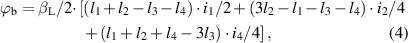
Figure 2(a) shows the normalized critical current ic1 vs. ϕext, calculated for five different values of i2 = 0, ±0.6 and ±1.2. This graph agrees very well with figure 2(b) of [28]. The dependence ic1 vs. i2 is shown in figure 2(b) for three values of ϕext = 0, 0.25 and 0.5 and both polarities of i1. This graph can be compared with figure 3 of [28]. While the overall agreement is very good, there is a difference for i2 < −1.5 (at ic1 > 0), where ic1 in our dynamic simulations shows an increase with decreasing i2, while ic1 in [28] continues to decrease, as indicated by the dashed blue and green lines in figure 2(b).

Figure 2. Simulations for comparison to results of [28] for a symmetric 4JJSQ (ak = 1) with βL = 1 and Γ = 10−6. (a) ic1 vs. ϕext for 5 different values of i2. (b) ic1 vs. i2 for three different values of ϕext. Differences to [28] occur in (b) at positive bias currents and i2 values below −1.5. In this region, dashed lines indicate ic1 vs. i2 as obtained in [28].
Download figure:
Standard image High-resolution imageThe differences can be understood from the IVC shown in figure 3(a) for i2 = −2 and ϕext = 0. The current i1 was swept in steps of 0.02 using the sequence 0 → 6 → −6 → 0. The SQUID IVC vSQ vs. i1 shows a clear supercurrent up to i1 = 1.96 at positive bias. However, when plotting the individual voltages vk across junctions 1–4 vs. current i1 (figure 3(b)) one finds that for currents between 0.06 and 1.96 junctions 1 and 2 are in the resistive state with compensating voltages v1 and v2, while the time-averaged voltages across junctions 3 and 4 are zero. This dynamic state could not be captured by the static analysis of [28].
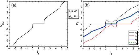
Figure 3. Simulations for a symmetric 4JJSQ (ak = 1) with βL = 1 and Γ = 10−6, for i2 = − 2 and ϕext = 0. (a) SQUID IVC vSQ vs. i1. (b) Individual voltages of the four JJs, vk vs. i1.
Download figure:
Standard image High-resolution imageAs another remarkable dynamic feature, figure 4(a) shows IVCs (for i2 = 0) for different ϕext = 0 (black line), 0.25 (red line) and 0.5 (green line). For ϕext = 0 and 0.25 the IVCs are hysteretic, although βC was set to zero. One further notes in figure 4(a) that in the resistive state at fixed bias current the voltage vSQ across the SQUID decreases with increasing flux, opposite to the case of a standard (2-JJ) dc SQUID and somewhat reminiscent to the case of a dc SQUID with nonzero βC, if the LC-resonance-voltage of the SQUID is exceeded [33, 34]. This is more clearly visible in figure 4(b), which shows vSQ(ϕext) curves for different values of i1. Here we initialized the phases δk and voltages uk with zero at a fixed value of i1 and then swept ϕext from either −1 to 1 or from 1 to −1. For i1 = 1.5, vSQ(ϕext) has maxima at ϕext = ± 0.5. With further increasing i1, those are converted into minima. From figure 4(a) we see that there is a resistive (downsweep) branch in the IVC also near integer values of ϕext (with a return current to the zero-voltage state ir1 = 0.88 at ϕext = 0), which however, could not be stabilized for i1 < 1.7 in our sweeps of ϕext. For i1 = 1.7 it appears only on the beginning of the sweep sequence. Also note that for i1 > 2.6 there is a splitting of the vSQ(ϕext) curves near half-integer values of ϕext. We did not investigate this feature further at this point.
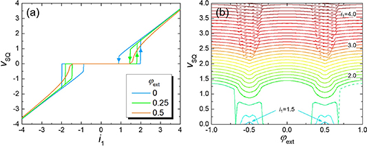
Figure 4. Simulations for a symmetric 4JJSQ (ak = 1) with βL = 1 and Γ = 10−6 for i2 = 0. (a) IVCs for different values of applied flux. Arrows indicate sweep direction. (b) Family of vSQ(ϕext) curves (solid lines: ϕext from −1 to +1; dashed lines: ϕext from +1 to −1) for different bias currents i1 (from 1.4 to 4.3 in 0.1 steps).
Download figure:
Standard image High-resolution imageWhile for i2 = 0 at given bias current i1 the time-averaged voltages vk across all junctions are identical (not shown here), a difference shows up when inspecting the time-dependent voltages uk , as displayed in figure 5 for i2 = 0 and i1 = 1.8. Figure 5(a) shows the case ϕext = 0. Junctions 1 and 2, as well as junctions 3 and 4, oscillate in-phase. However, the voltage oscillations of the junctions 1 and 2 in the left and 3 and 4 in the right arm of the SQUID are out-of-phase, corresponding to a large circulating current around the SQUID. Consequently, the effective critical current ic1 is lowered compared to the static case, causing the hysteresis in the IVC. Note that for a symmetric two-junction SQUID the circulating current would be zero for ϕext = 0.

Figure 5. Simulation of time-dependent voltage oscillations of all 4 single JJs of a symmetric 4JJSQ (ak = 1, βL = 1 and Γ = 10−6) at i2 = 0 and i1 = 1.8 for ϕext = 0 (a), 0.25 (b) and 0.5 (c).
Download figure:
Standard image High-resolution imageIn figure 4(a), we show that the hysteresis in the IVC decreases and eventually vanishes with increasing ϕext. More precisely, the hysteresis disappears near ϕext = 0.314. Figures 5(b) and (c) show uk (t) for ϕext = 0.25 and 0.5, respectively. At ϕext = 0.25 (figure 5(b)) the phase shift between the JJs in the left and right arm becomes smaller. If we increase ϕext further to ϕext = 0.5 (figure 5(c)), the system seems to become chaotic, and synchronization of JJs within the same SQUID arm gets lost. This chaotic regime seems to coincide with the region where the IVCs are no longer hysteretic. We also calculated families of vSQ (ϕext) curves for i2 = ± 0.6 and ±1.2 (not shown). In all cases we observed instabilities in the vSQ (ϕext) patterns indicating that for the symmetric device chaotic regimes appear over a wide range of i2 values.
Trivially, if the critical currents of one of the junctions in each arm of the SQUID were much bigger than the critical currents of the two other junctions one should return to the behaviour of a 2-junction SQUID. Thus, to investigate the quite unusual hysteresis in the IVCs (in the absence of JJ capacitance or heating effects) in some more detail we also show simulations for a somewhat asymmetric 4JJSQ with a1 = a3 = 1.2 and a2 = a4 = 1. The parameters are chosen such that the left and right arm of the SQUID remain symmetric.
Figure 6(a) shows by the red line ic1 vs. ϕext for the asymmetric case in comparison to the symmetric case (black line). In both cases, the critical current has a maximum ic1,max = 2 at ϕext = 0 and minima ic1,min at ϕext = ±0.5, like for a symmetric 2-junction SQUID. But one notes that the modulation depth (ic1,max − ic1,min)/ic1,max of the asymmetric 4JJSQ is larger than for the symmetric 4JJSQ and closer to the modulation depth of 1/2 which would be obtained for a symmetric 2-junction SQUID with βL = 1.
Figure 6. Simulations (βL = 1, Γ = 10−6, i2 = 0), comparing ic1(ϕext)-curves for a symmetric (black line) and slightly asymmetric (red line) 4JJSQ.
Download figure:
Standard image High-resolution imageFigure 7(a) shows IVCs for the asymmetric 4JJSQ for ϕext = 0 (maximum ic1) and 0.5 (minimum ic1). For ϕext = 0 the critical current ic1 = 2, i.e. the two weaker JJs 2 and 4 (with a = 1) are switching to the resistive state. With further increasing i1, we find a jump to higher vSQ at i1 = 2.4, which means that now also JJs 1 and 3 (with a = 1.2) become resistive. We also find for the slightly asymmetric 4JJSQ a hysteretic IVC for ϕext = 0; however, this is smaller than for the symmetric 4JJSQ, and it is also suppressed with increasing ϕext. In the resistive state one observes a crossover between the two IVCs at ϕext = 0 and 0.5.
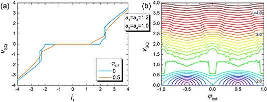
Figure 7. Simulations (βL = 1 and Γ = 10−6, i2 = 0) for slightly asymmetric 4JJSQ (a1 = a3 = 1.2; a2 = a4 = 1). (a) IVCs at two different values of applied flux. (b) Family of vSQ(ϕext) curves for different bias currents i1 (from 1.4 to 4.4 in 0.1 steps). ϕext is swept from −1 to 1.
Download figure:
Standard image High-resolution imageFigure 7(b) displays for the slightly asymmetric 4JJSQ a family of vSQ(ϕext) curves for different bias currents i1. Like for the symmetric 4JJSQ, at low bias currents the voltage maximum occurs at half-integer values of ϕext. With increasing i1 one observes the crossover to the state where the maxima of vSQ vs. ϕext occur at integer values of ϕext. Also note, that near the crossover the vSQ vs. ϕext curves look noisy. This is because of the small hysteresis visible in the IVCs.
Finally, for the symmetric device, we also address the case of higher thermal noise. We take Γ = 4.4 · 10−3, a value, which we find for our experimental 4JJSQ discussed below. Figure 8(a) shows IVCs for ϕext = 0, 0.25 and 0.5. The large hysteresis observed for Γ = 10−6 has nearly vanished, and we observe a low-bias region where the voltage at ϕext = 0.5 is higher than the voltage for lower values of ϕext. This can also be seen in the vSQ vs. ϕext curves displayed in figure 8(b), where one observes the crossover in the position of voltage maxima from half-integer to integer values of ϕext at voltages near 1. Also note that the voltage jumps associated with the splitting of the vSQ(ϕext) curves at high bias currents are no longer observable.
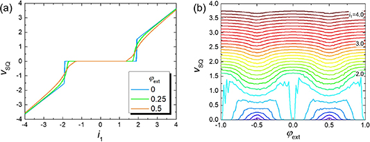
Figure 8. Simulations for a symmetric 4JJSQ (ak = 1) with i2 = 0, βL = 1 and Γ = 4.4 · 10−3. (a) Simulated IVCs for different values of applied flux. (b) Family of vSQ(ϕext) curves for different values of bias current i1 (from 1.4 to 4.1 in 0.1 steps). ϕext is swept from −1 to 1.
Download figure:
Standard image High-resolution image3. Fabrication and measurement results
3.1. Fabrication and design
The 4JJSQs with deep submicron sandwich-type trilayer SNS JJs with Nb electrodes and HfTi barrier were fabricated using an established Nb planar fabrication technology. This is based on magnetron sputtering deposition on 3 inch Si wafers with 300 nm thermally oxidized SiO2, electron beam lithography to ensure high alignment precision for nanopatterning of the small features of our SQUIDs and a chemical-mechanical polishing step to planarize the insulating SiO2 layer between the Nb base and the Nb wiring layer and to open contact windows between the Nb top layer and Nb wiring layer. Those technologies are available at the clean room center at PTB Braunschweig and have been applied before to the fabrication of JJ-based circuits [35–38], including complex and advanced nanoSQUID layouts, such as gradiometers [39] and 3-axis vector nanoSQUIDs [40] and for auxiliary components such as pick-up and feedback coils. Since the fabrication technology is not the focus of this paper, we refer to [41] for the detailed fabrication technology.
We fabricated dc SQUIDs with four SNS JJs with nominal lateral JJ size of 300 nm × 300 nm (figure 9) and a normal conducting Hfwt50%Tiwt50% (HfTi) barrier with a thickness of 26 nm. The superconducting Nb loop is constructed as two quadrants in the 160 nm thick Nb base layer which are connected via the four JJs to two more quadrants in the Nb wiring layer, which has a thickness of 200 nm. The applied magnetic flux ϕext to the SQUID can be provided by the modulation currents Imod,i (i = 1–4) through four inductively coupled modulation lines in the Nb base layer, which are designed to be in a close distance (with a nominal 0.9 µm gap) to the four SQUID loop segments. The SQUID loop was designed to have an inner diameter of 8.0 µm with 1.1 µm linewidth for the Nb base and 8.1 µm diameter with 0.9 µm line width in the wiring layer.
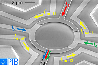
Figure 9. Scanning electron microscopy image of a 4JJSQ. Two superconducting quadrants in the Nb base layer are connected via four JJs to two quadrants in the Nb wiring layer. The bias current I1, drain current I3, control currents I2 and I4 and modulation currents Imod1 to Imod4 are indicated by arrows. The voltage across the 4JJSQ is measured between the ports 1 and 3 for bias current I1 and drain current I3, respectively.
Download figure:
Standard image High-resolution image3.2. Basic SQUID characterization
All measurement data shown here were taken at liquid He temperature (T = 4.2 K) and we used the current I1, flowing from the top across the SQUID loop to the drain (bottom; see figure 9) as the bias current. The SQUID voltage VSQ was measured between ports 1 and 3. The modulation current Imod1 was used to inductively couple magnetic flux Φ1 to the SQUID loop, via the mutual inductance M1 = Φ1/Imod1. The control current I2, flowing from the left to the drain, was used to shift the interference patterns. We always kept I4 = 0, and accordingly, I3 = I1 + I2. Also, we limit the results presented below to one exemplary 4JJSQ, since the other investigated 4JJSQs showed similar behaviour.
The IVCs VSQ(I1), with Imod1 adjusted to obtain maximum critical current Ic1,max and minimum critical current Ic1,min are shown in figure 10(a) for the 4JJSQ with I2 = 0 and 37.5 µA. These IVCs, as well as all others we obtained, are nonhysteretic. For I2 = 0 the maximum critical current is 80 µA, which corresponds to I0 ≈ 40 µA and a critical current density j0 ≈ 44 kA cm−2. For the noise parameter we find Γ ≈ 4.4 · 10−3 at 4.2 K. Further, we find the best overall agreement between the shapes of the experimental and simulated IVCs for i2 = 0 by using I0 R = 15 µV.
We show in figure 10(b) the voltage oscillation VSQ(Imod1) for the 4JJSQ (with I2 = 0) at I1 = 80 µA. From the oscillation period (current Imod1,0 required to couple one flux quantum Φ0 to the SQUID) we determine the inverse mutual inductance 1/M1 = Imod1,0/Φ0 = 1.95 mA/Φ0 (M1 = 1.06 pH) between the corresponding modulation line and the 4JJSQ. The maximum modulation voltage of our 4JJSQ is 9 µV (cf figure 10(b)) and the derived maximum transfer coefficient is VΦ ≈ 50 µV/Φ0. Using the simulation software 3D-MLSI, to calculate the supercurrent density distribution based on the London equations [42] for the given geometry of our device and with a London penetration depth λL = 70–80 nm for our Nb thin films, we obtain for the mutual inductance M1 = 1.12 pH, which is in good agreement with the value M1 = 1.06 pH determined experimentally from figure 10(b). For the SQUID inductance we calculate with 3D-MLSI L = 17.0 pH, leading to an estimated screening parameter βL = 2I0 L/Φ0 ≈ 0.66. From direct simulations (see below) we obtain βL = 0.65 and L = 16 pH, which is in very good agreement.
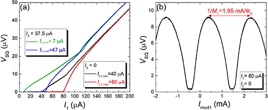
Figure 10. Experimental results for the 4JJSQ at 4.2 K. (a) IVCs with Imod1 adjusted to achieve maximum (Ic,max) and minimum (Ic,min) critical current for I2 = 0 and 37.5 µA. (b) Voltage vs. modulation current for I2 = 0 (chosen to obtain maximum voltage modulation amplitude).
Download figure:
Standard image High-resolution imageTo work with dimensionless quantities for comparing our measurement results with calculations from [28] and with our simulations based on the mathematical model described in section 2, we normalize the currents I1 and I2 to I0 and the modulation current Imod1 to Imod1,0 = Φ0/M1. The voltages are normalized to I0 R = 15 µV. We denote normalized quantities by lower case letters i and v. ϕ1 = Imod1/Imod1,0 = Φ1/Φ0 is the normalized applied flux (modulation current).
For the simulations shown below we use asymmetry parameters a1 = 1.05 and a4 = 0.95, so that we have a1 + a4 = 2 for the weakest JJs in both SQUID arms. We further use a2 = 1.15 and a3 = 5 and βL = 0.65. These values have been obtained by matching ic1 vs. ϕ1 curves for i2 = 0 and i2 = 1.25, as well as IVCs for i2 = 0 and ϕ1 chosen so that the positive critical current was at a maximum or a minimum. Parameters a1 to a4, as well as βL were varied in steps of 0.05. For the asymmetry parameter a3 we can give only a lower limit of 4 and for convenience set this parameter to 5. We briefly note here that, by inspecting IVCs for i4 = 0 only, in the absence of measurements of the individual voltages vk , we could have exchanged the values of a3 and a4 without changing the results. However, using the measured individual junction voltages, as well as using measurements with nonzero values of the current i4, we find JJ3 to be the junction with significantly higher asymmetry parameter. In experiment the threshold voltage to determine the critical current was 1 µV, translating to a normalized voltage criterion of about 0.07 to determine ic1 in our simulations. Finally, we note that to match experimental ic1(ϕ1) or vSQ(ϕ1) curves with simulations, the experimental Imod-axes needed to be adjusted typically by an offset of 0.05–0.1 mA to account for residual fields of ≈1–2 µT in the cryostat.
Figure 11 shows by solid lines the measured quantum interference patterns ic1(ϕ1) of our 4JJSQ together with the corresponding simulated curves (dashed lines). Here we measured IVCs for 101 different values of the modulation current, varying between Imod1 = −1.48 mA and 2.40 mA, at 5 different values of the applied control current i2, which were chosen to be between −1.25 and 1.25.

Figure 11. Measured (solid lines) and simulated (dashed lines) ic1(ϕ1) curves of the 4JJSQ for 5 different control currents i2. The boxes to the right indicate the values for the parameters used in the simulations.
Download figure:
Standard image High-resolution imageAs predicted by the model described in [28], the quantum interference patterns in figure 11 are not only shifted to lower critical currents, but also along the ϕ1-axis while applying a positive control current (i2 > 0). For negative control currents (i2 < 0) the patterns are shifted only along the ϕ1-axis, which agrees with the theoretical model, too. Compared to [28] and to our simulations for symmetric 4JJSQs (cf figure 2(a)) we observe a shift of all quantum interference patterns to the left, which is due to the asymmetry in the junction critical currents of our device.
Now, we compare our simulation results to IVCs measured at different values of applied flux and i2 = 0. The measured curves are presented in figure 12(a), whereas the simulated curves are shown in figure 12(b). In general, there is a good agreement between the measurement and the simulation. Particularly, the measured critical current values and the 'bends' (abrupt changes in the slope) observed in the IVCs for different values of applied flux could be reproduced by simulations.
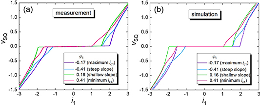
Figure 12. (a) Measured and (b) simulated (same parameters as in figure 11) IVCs for i2 = 0 and different values of applied flux to reach either maximum or minimum ic1 or to stay on the steep or shallow slope of the ic1(ϕ1) pattern (for i1 > 0; cf figure 11).
Download figure:
Standard image High-resolution imageAn explanation for the bending of the IVCs can be found by having a closer look at the voltages vk across the four individual junctions, shown in figure 13 for i2 = 0. The left panels (a), (c) show measurements and the right panels (b), (d) show simulations. The upper panels (a), (b) show vk (i1) at maximum critical current (at ϕ1 = −0.17), and the lower panels are for minimum critical current (at ϕ1 = 0.41). In both cases, JJ3 stays in the zero-voltage state. The voltage v1 across JJ1 equals v4 as long as JJ2 is in the zero-voltage state, while v1 is close to v2 as soon as v2 becomes nonzero. This transition marks the bends in the IVCs shown in figure 12, where the voltages are the sum of the JJs in the right and left arm, respectively.
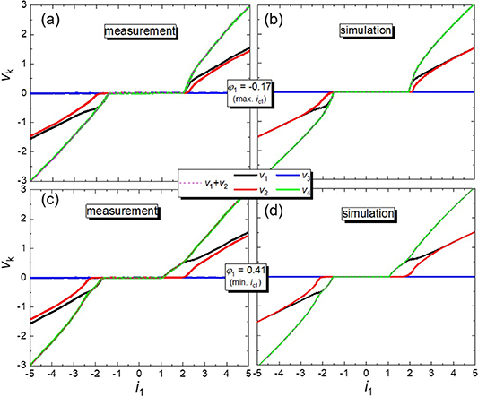
Figure 13. (a), (c) Measurement and (b), (d) simulation (same parameters as in figure 11) of the voltages vk (i1) of the individual four junctions of the 4JJSQ for i2 = 0 and an applied flux leading to maximum (a), (b) and minimum (c), (d) critical current (solid lines). Dashed lines show the total voltage across the SQUID.
Download figure:
Standard image High-resolution imageWith respect to the IVCs we briefly mention that also for nonzero values of i2 we found a very good agreement between experiment and simulation. However, neither in experiment nor in simulation we found hysteretic IVCs for our strongly asymmetric device, as we found in our simulations for the (nearly) symmetric 4JJSQ, cf figures 4–6.
Figure 14 shows measured (figure 14(a)) and simulated (figure 14(b)) families of vSQ(ϕ1) curves for i2 = 0. Here, we varied the bias current i1 in steps of 0.1 from 1 to 4 for positive bias and from −1 to −4 for negative bias.
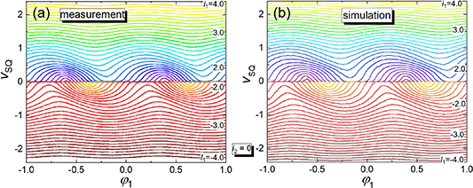
Figure 14. Families of (a) measured and (b) simulated (same parameters as in figure 11) vSQ(ϕ1) curves for different values of the bias current i1 (|i1| from 1.0 to 4.0 in 0.1 steps) and for control current i2 = 0.
Download figure:
Standard image High-resolution imageThe vSQ vs. ϕ1 curves show a point-symmetric behaviour and for |i1| ≲ 1.5 one observes the voltage maxima at half-integer values of the applied flux (shifted due to the asymmetric JJs), similar to 2-junction SQUID behaviour. For higher values of the bias current |i1|, the maxima of the vSQ(ϕ1) curves are gradually shifting further to the left and right, for positive and negative i1, respectively. The simulations are in good agreement with the experimental data. As we neglected inductance and resistance asymmetries in the simulations, the above-described shifts in the voltage maxima are attributed to critical current asymmetries only. Note that in contrast to the simulated vSQ(ϕext) families shown in figures 4, 7 and 8, we do not observe an abrupt crossover of the position of the voltage maxima from half-integer to integer values of the applied normalized flux. Further note that in contrast to the case of the simulated vSQ(ϕext) families for the symmetric 4JJSQ with comparable noise parameter, the vSQ vs. ϕ1 curves look much less noisy close to vSQ ≈ 1, which is consistent with the missing hysteresis in the IVCs of our asymmetric device.
Figure 15 shows measured (figure 15(a)) and simulated (figure 15(b)) vSQ(ϕ1) curves for i2 = 0 and ±0.95 while the bias current is chosen to obtain maximum voltage modulation amplitude. We observe a shift of the curves along the ϕ1-axis while applying a positive control current (i2 = 0.95) as well as negative control currents (i2 = −0.95) compared to the case of i2 = 0. In contrast to the symmetric device, no instabilities appear in the curves.

Figure 15. (a) Measured and (b) simulated vSQ(ϕ1) curves for different values of control current i2 and bias current i1 (chosen to obtain maximum voltage modulation amplitude).
Download figure:
Standard image High-resolution image3.3. Critical current vs. i2
Figure 16 displays the measured (a) and simulated (b) critical currents ic1 vs. control current i2 for both polarities of ic1 and different values of applied flux (taking into account that for i2 = 0 the ic1(ϕ1) curves have their maximum at ϕ1 = −0.17 for ic1 > 0, and at 0.16 for ic1 < 0. The agreement between the measured and the simulated curves is very good and, like for the symmetric case (cf figure 2(b)), we observe both in experiment and simulation an increase of the critical current for positive bias, for i2 < −1.5 and ϕ1 adjusted to be near the ic1(ϕ1) maximum for i2 = 0.

Figure 16. Comparison between (a) measured and (b) simulated (same parameters as in figure 11) ic1(i2) curves for different values of applied flux. The blue curves correspond to applied flux values which yield maximum ic1 in the ic1(ϕ1) curves for i2 = 0. For the green and orange curves, ϕ1 is increased by approximately ¼ and ½, respectively.
Download figure:
Standard image High-resolution imageThe upper panel of figure 17 displays experimental (a) and simulated (b) IVCs vSQ(i1) for i2 = −2 and the same three values of ϕ1 that were chosen for the ic1(i2) curves in figure 16 for ic1 > 0. Again, the agreement between experiment and simulation is very good. The lower panel of figure 17 shows measured (c) and simulated (d) individual junction voltages vk (i1) for ϕ1 = 0.31 and i2 = −2. Like for the symmetric case, cf figure 3(b), the simulations yield a state where the junctions in the left arm are resistive, with opposite dc voltages, while the junctions in the right arm remain in their zero-voltage state. This state is also realized in the experimental device.

Figure 17. Measured (a) and simulated (b) IVCs vSQ(i1) for i2 = −2 and three values of ϕ1 and measured (c) and simulated (d) individual junction voltages vk (i1) for i2 = −2 and ϕ1 = 0.31. For the simulations, same parameters as in figure 11 were used.
Download figure:
Standard image High-resolution image3.4. Current-phase relation
As explained in [28] the current-phase relation F(δ) of junctions 1 and 2 can be reconstructed from measurements of the critical current ic1(ϕ1,i2). For a given value of i2 one determines the flux value ϕ1 where ic1(ϕ1) has a maximum. This constitutes the curve ϕ1,max(i2) which encodes the CPR of JJ1 for i2 > a2 − a1 and the CPR of JJ2 for i2 ⩽ a2 − a1.
For junction 2 the phase δ2 is found from:

and the normalized CPR F2(δ2)/I0 is obtained via:

The phase µ is a constant and can, e.g. be determined by demanding F2(0) = 0.
From equation (3), using the definition of jSQUID and further assuming sinusoidal CPR's and under the assumption that junction 4 is at its critical current we can also give an analytic expression for µ,

For junction 1 one makes the replacements i2 → −i2, a1 ↔ a2, δ2 → δ1, and for µ one finds:

Figure 18(a) shows a measured contour plot ic1(ϕ1,i2). Here, we measured IVCs for 52 different values of ϕ1 from −0.9 to 1 for 81 different values of i2 between −2 and 2. ϕ1,max(i2) is indicated by the pink symbols for ϕ1 between −0.25 and 0.3 and for both polarities of i2. The reconstructed normalized CPRs Fi (δi )/(aiI0) are shown in figure 19(a) for junction 1 and in figure 19(b) for junction 2. In the graphs we also plotted by lines the sinusoidal dependences. For the phase shift we used µ = −0.22 for junction 1 and µ = −0.12 for junction 2, to fulfil F1(0) = F2(0) = 0. Apparently, the data points are compatible with a sinusoidal CPR, although the error bars are large. Using the sinusoidal CPRs we also inverted equations (5) and (6) and show the resulting ϕ1,max(i2) curves as solid white lines in figure 18(a).

Figure 18. (a) Measured and (b) simulated (same parameters as in figure 11) contour plot ic1(ϕ1,i2) for the 4JJSQ. Pink dots indicate the maxima of the ic1 vs. ϕ1 patterns at fixed values of i2, i.e. ϕ1,max(i2). The white solid lines are calculated by inverting equations (5) and (6) for sinusoidal CPRs for junctions 1 and 2. Values of i2 > a2 − a1 are for junction 1 while values of i2 ⩽ a2 − a1 are for junction 2.
Download figure:
Standard image High-resolution image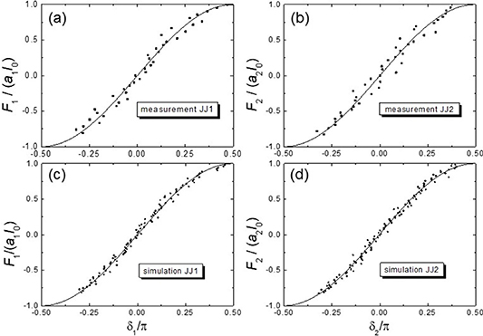
Figure 19. CPRs of JJ1 (a) and JJ2 (b), extracted from measured ϕ1,max(i2) data. CPRs of JJ1 (c) and JJ2 (d), extracted from the simulated ϕ1,max(i2) data. Lines correspond to sinusoidal CPRs F1/(a1 I0) = sin δ1 and F2/(a2 I0) = sin δ2.
Download figure:
Standard image High-resolution image
Finally, for completeness and in order to further test the evaluation method we applied the same procedure for the simulated ic1(ϕ1,i2) curves, where by ansatz we have sinusoidal CPRs. Figure 18(b) shows the corresponding contour plot ic1(ϕ1,i2). In the calculations both ϕ1 and i2 were varied in steps of 0.02.
Figures 19(c) and (d) show the extracted CPRs, where we used µ = 0 for JJ1 and µ = 0.1 for JJ2 to fulfil F1(0) = F2(0) = 0. Those values are close to µ = −0.01 and 0.09, found from equations (7) and (8), respectively. We further note that the experimental data yield values for µ that are shifted by Δµ = −0.22 relative to the simulated ones. This may indicate that a3 of the experimental device is much larger than the value of 5 used for simulation. Indeed, a3 → ∞ would roughly lead to the observed value of Δµ.
4. Conclusions
Motivated by the fact that the multi-terminal, multi-junction SQUID, suggested and realized for the SQUID-on-tip configuration, is also an interesting concept for other highly miniaturized SQUIDs we fabricated four-terminal, four-junction SQUIDs, using Nb SNS-junctions with a HfTi barrier. Like the conventional two-junction dc SQUID, also this device can be very well modelled using RCSJ-type equations, and we see that the static behaviour is similar to that of the 4-junction SQUID-on-tip. Particularly in the resistive state the dynamics of the device can strongly differ from the dynamics of a conventional dc SQUID, involving various phase-locked and chaotic states if the 4-junction SQUID is symmetric. We have addressed several examples. While the symmetric device may be interesting for studies of nonlinear dynamics, the appearance of chaos and of instabilities in the current–voltage characteristics and the voltage-flux patterns is clearly detrimental for SQUID magnetometry. However, these effects have disappeared in the asymmetric 4-junction SQUID studied experimentally. Under this condition, as judged from the transport characteristics, the multi-terminal, multi-junction configuration is a promising geometry, allowing for a stable in-situ control over shifting interference patterns. This may become particularly important when it comes to pushing the limits of miniaturization, which will make it increasingly difficult to optimally flux-bias the conventional two-junction dc SQUID. However, it remains to be investigated, how the 4-junction dynamics imprints on the noise properties of the SQUID.
Acknowledgments
The authors thank K Störr, M Petrich, R Gerdau and P Hinze for their help throughout the wafer fabrication and support at the SEM equipment.
We gratefully acknowledge financial support by the Deutsche Forschungsgemeinschaft (DFG) (KI 698/3-2, KO 1303/13-2), by the European Commission under H2020 FET Open grant 'FIBsuperProbes' (Grant No. 892427) and by the COST action NANOCOHYBRI (CA16218). This work was partially funded from the EMPIR programme (Project ParaWave 17FUN10) co-financed by the Participating States and from the European Union's Horizon 2020 research and innovation programme.
Data availability statement
The data that support the findings of this study are available upon reasonable request from the authors.