

Abstract
Biaxially textured FeSe0.5Te0.5 (FST) thin films were fabricated on ion-beam assisted-deposition LaMnO3 (LMO) buffered metal substrate with additional CeO2 as a buffer layer. Profiting from the implementation of CeO2 layers, the resultant FST films show a small out-of-plane misalignment of about 2.04° and an in-plane misalignment around 4.02°. In addition, the films have a high superconducting transition temperature (Tc) ∼ 17 K and a comparatively high critical current density (Jc) of 0.78 MA cm−2 in self-field at 4.2 K. On the other hand, a high Jc peak for H//c above H//ab at temperatures below 10 K was observed, which results from grain boundaries along the c-axis. In addition, Jc peaks for H//ab emerge above 10 K and become more pronounced than those for H//c at 12 K, indicating both a temperature- and field-dependent pinning mechanism. Moreover, Jc(θ) data except for in the vicinity of H//ab and H//c can be successfully scaled using the anisotropic Ginzburg–Landau approach with an appropriate Jc anisotropy ratio of γJc ∼ 1.5, implying the presence of both ab-plane and c-axis correlated flux pinning centers in FST films.
Export citation and abstract BibTeX RIS
1. Introduction
Iron-based superconductors (IBSs) first discovered by Kamihara et al [1] are considered to be potential materials for applications particularly in the high-field region since they possess a relatively high Tc up to 55 K, a high upper critical field (Hc2) larger than 100 T, and a low Hc2 anisotropy close to 1 at low temperatures [2]. Compared to other IBS families, the iron chalcogenide FeSex Te1−x (also called 11 compounds) are attractive due to their simple crystal structure and the absence of toxic or volatile elements, which together contribute to a relatively safe synthesis process, despite their lower Tc (in the order of 20 K) [3]. The FeSex Te1−x superconductor has received much attention in both basic physics and high-field applications. Various studies have shown the tunability of the superconducting properties in FeSex Te1−x superconductor. For example, a Tc as high as 109 K in single-layer films of FeSe grown on a conductive SrTiO3 substrate displays strong potential for practical applications [4]. In addition, a tunable Tc ranging from 18 K to a maximum of 35 K in FeSe0.5Te0.5 film was achieved using an ionic-gating approach [5]. Very recently, it has been reported that the Tc of the FeSe single crystal can be enhanced up to 37 K by pressure quenching, and more importantly, the pressure-enhanced superconductivity can be stabilized without retaining external pressure [6]. On the other hand, in recent years much effort has been devoted to realizing FeSex Te1−x tapes and eventually applications in high-field, by exploiting the ex situ powder-in-tube (PIT) method, superconducting tapes composed of 11 phase have been prepared and yield of Jc reaching about 104 A cm−2 at 5 K [7], the Hc2 of which is estimated to be about 25 and 33 T for the field perpendicular and parallel to the tape surface, respectively. Although the PIT method is regarded as an economical way of superconducting wire fabrication, it is worth noting that 11 phase exhibits serious problems in terms of the chemical compatibility to metal sheaths, and the reaction between 11 phase and the metal sheath has an adverse effect on the superconducting properties of the wire. This further demonstrates the necessity of employing the coated conductor (CC) route for applications of the 11 compounds [8]. Currently, the techniques prevalently used for second-generation (2G) high-temperature superconducting oxide tapes are ion-beam assisted deposition (IBAD) [9] and rolling assisted biaxially textured substrates (RABiTS) [10], and these two techniques are also applicable to the 11 compounds because of their comparable in-plane lattice constants with YBCO [11].
Many works have been carried out in respect of FeSex
Te1−x
CCs. In spite of the large lattice mismatch between FST and MgO (aFST = 3.81 Å, aMgO = 4.21 Å), Si et al successfully obtained a textured FST thin film on the IBAD-MgO templates, which carried an almost isotropic Jc > 104 A cm−2 at 4.2 and 25 T [11]. To overcome the lattice mismatch, a CeO2 buffer layer was adopted, and the resultant film achieved a Jc ∼ 0.1 MA cm−2 at 4.2 and 30 T. The CeO2 buffer layer, which has a lattice parameter (aCeO2/ = 3.82 Å) comparable to that of FST (aFST = 3.801 Å), was regarded as the key factor in improving the Jc–H properties of the FST film [12]. Despite the large in-plane misalignment (Δφ = 7.8°) for IBAD-LaMnO3 (LMO) metal substrate, the FST thin film fabricated on it still shows a Jc over 0.35 MA cm−2 at 4.2 K, 9 T, for which the Hc2 is estimated to be about 87 T (H//ab) and 76 T (H//c) [13]. In addition, a novel electrochemical deposition technique was employed to grow FeSe films on RABiTS tapes, in which a low Tc of 2.5 K was observed, indicating that further optimization is needed [14, 15]. In order to reduce the preparation costs of FST CCs, Sylva et al prepared FST thin films on commercially available Ni—5 at% W tapes, with only one CeO2 buffer layer presented, acting as a chemical barrier against Ni diffusion. The resultant FST CCs show a Tc of 16 K, while the Jc reaches 0.17 MA cm−2 at 4.2 K in self-field, which is reduced by an order of magnitude at 18 T [16]. Moreover, they also studied the effect of texture and thickness of the buffer layers on the superconducting characteristics of FST CCs [17], and found that the best FST films were obtained on the RABiTS with highly textured CeO2 layer of 350 nm. In comparison, a Jc ∼ 1.2 × 10⁴ A cm−2 was also obtained for the FST thin film deposited on the HASTELLOY® C276 substrate with only a randomly oriented oxide overlayer of about 400 nm in thickness. As a result, they concluded that the texture and thickness of the buffer layers have a significant effect to the final superconducting properties of the FST CCs.
Using the IBAD technique, biaxially oriented buffer layers can be formed on polycrystalline Ni-based alloy (i.e. metal substrates, which allow the subsequent deposition of superconducting thin films). These buffer layers should reach a suitable in-plane texture, which will contribute to good superconducting performance for FST thin films. In this work, using a less well-textured IBAD-LaMnO3 substrate with a larger in-plane misalignment ΔφLMO ∼ 6.69°, we successively deposited a CeO2 layer as well as FST thin film via pulsed laser deposition (PLD) [13], and the Jc properties of the FST CCs as a function of magnetic fields in different orientations were studied. The comparable in-plane lattice parameter of CeO2 with FST provides a much smaller lattice mismatch than the LMO buffer layer, producing a better in-plane texture in FST CCs. Accordingly, the resultant FST thin films possess good superconducting performance, such as an improved Jc of up to 0.78 MA cm−2 at 4.2 K in self-field, a slightly enhanced Tc of 17 K, a higher Hc2 and Hirr, compared to previous results [13]. In order to investigate the anisotropy of Jc and magnetic flux pinning in FST films, we measured the angular dependence of Jc at various fields and temperatures. A maximum Jc at θ = 180° (H//c) is observed in the low-temperature region, and a maximum Jc at θ = 90° (H//ab) emerges in the high-temperature and high-field region. This indicates that the dominant pinning mechanism in the FST CCs is temperature- and field-dependent. Based on high-resolution transmission electron microscopy (TEM) images and pinning force analysis, we propose that grain boundaries (GBs) are responsible for the c-axis correlated flux pinning, and the intrinsic pinning arising from coupled ab planes also plays a role in the achievement of the good Jc property of the FST CCs.
2. Experiment details
A KrF excimer laser (wavelength: 248 nm, repetition rate: 3 Hz) was utilized for the PLD of epitaxial CeO2 intermediate layers and FST thin films on IBAD-LMO-buffered metal tapes. The nominal composition of the target prepared by solid-state reaction is Fe:Se:Te = 1:0.5:0.5 [18] and the CeO2 target was provided by Advanced Technology and Materials Co., Ltd. During the sample preparation process, the distance between the substrate and target was kept at 40 mm and the vacuum was kept lower than 10−7 Torr. The deposition of FST CCs consists of two steps. First, the CeO2 interlayer was grown at 750 °C with a laser energy of 330 mJ per pulse. After the CeO2 buffer layer was cooled down to 450 °C at a rate of 10 °C min−1, the FST thin film was deposited using laser energy of 320 mJ per pulse. Finally, the FST CCs were cooled to room temperature at the same rate as the CeO2. The thickness of the CeO2 buffer layer and FST thin film is controlled at around 460 and 200 nm, respectively, by modulating the deposition time. The microstructure of the films was investigated using x-ray diffraction (XRD; Bruker D8 ADVANCE) with Cu Kα radiation and TEM performed on a JEOL 2100F. For transport measurements, micro bridges 20 μm in width and 100 μm in length were fabricated by Ar+ etching after a photolithographic process. Electrical transport properties were investigated in a Physical Property Measurement System (quantum design) equipped with a sample rotator by a standard four-probe method. The two middle electrodes are voltage terminals, and the other two are current terminals. A small DC of 10 μA was utilized for resistivity measurements in a field applied parallel or perpendicular to the film surface. We obtained Jcs from current–voltage (I–V) curves using a criterion of 1 μV cm−1. In the angular-dependent Jc measurements, the magnetic field H was applied in maximum Lorentz force configuration (H⊥Ic, where Ic is the current) at an angle θ from the c-axis.
3. Results and discussion
Figure 1(a) illustrates the XRD patterns (θ−2θ, φ and ω scans) of the FST sample. Only (00l) peaks of the FST thin film could be detected, indicating that the film is c-axis oriented and has high phase purity. Compared with FST thin films directly deposited on less well-textured IBAD-LMO templates [13], the rocking curve of (002) reflection for the FST thin film in this work has a lesser full width at half maximum (FWHM) value, i.e. ΔωFST ∼ 2.044° shown in the inset. This is mainly due to the smaller FWHM value for the CeO2 buffer layer (ΔωCeO2 ∼ 1.053°). The out-of-plane lattice constant c = 5.974 Å was evaluated from the (001) reflection and the in-plane lattice constant a = 3.798 Å was calculated according to the relation 1/d101 2 = 1/a2 + 1/c2, both of which are larger than the corresponding values in [13]. We also performed in-plane φ-scans of the (101) diffraction for FST thin film and (202) diffraction for the CeO2 buffer layer, as shown in figure 1(b). It is evident that the films have explicit fourfold symmetric peaks, and the peaks from FST rotate 45° relative to the CeO2 layer, indicating an epitaxial growth of the FST film on the CeO2 layer following a relationship of (001)[100] film//(001)[110] buffer layer. It is the same in the case of FST thin films grown on CaF2 (00l) substrates [18]. The average FWHMs of the peaks from the FST thin film and CeO2 layer are ΔφFST ∼ 4.02° and ΔφCeO2 ∼ 4.88°, respectively. It is found that Δω as well as Δφ of the FST thin film is much reduced in comparison with the misalignment of LMO layer (ΔφLMO ∼ 6.69°) due to the existence of the CeO2 buffer layer, which conduces to a good biaxial texture for the FST thin film. Good matched crystal lattices of the film and the buffer layer are preferable for the film growth [19].
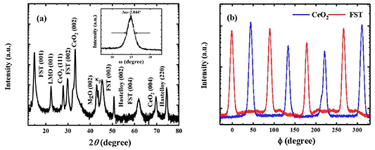
Figure 1. (a) θ/2θ pattern of FST thin films deposited on IBAD-LMO substrates with a CeO2 buffer layer. Rocking curve of the (002) reflection is shown in the inset. (b) φ-scans using the (101) reflection from the FeSe0.5Te0.5 thin films and the (202) reflection from the CeO2 layers.
Download figure:
Standard image High-resolution imageR–T measurements (10–300 K) were carried out for FST thin films and the results are exhibited in figures 2(a), while (c) and (d) show the details from 14 to 18 K. According to the statement of Yuan et al, this is the type of substrate and the crystallinity of films that determine the value of Tc, rather than the films' lattice constants [20]. Because of the better crystallinity in the FST thin film deposited on CeO2-buffered substrate, the film possesses a relatively high superconducting transition ∼17 K (Tc onset) and a small transition width (ΔTc) of 1.5 K. Furthermore, Tc shifts to lower temperature when the magnetic field increases from 0 to 9 T at both field orientations, i.e. H//ab (left) and H//c (right), and Tc zero decreases from 15.5 to 14.5 K (H//ab) and 14.1 K (H//c) at 9 T, respectively. A clear feature of the thermally activated vortex dynamics is the broadening of superconducting transition in the presence of an external magnetic field [21]. In addition, the vulnerability to thermal fluctuations in a superconductor can be evaluated by the Ginzburg number (Gi), which is defined as the ratio of the minimal condensation energy within the coherence volume and the thermal energy at Tc (kB Tc, where kB is the Boltzmann constant). Gi dictates the width of the critical fluctuation region around Tc (i.e. ΔTc ∼ GiTc) [22]. The broadening of the transition for H//c is more significant than for H//ab, which is typical of IBS with high Gi numbers [23]. Figure 2(b) shows Hc2 and Hirr of the film as a function of the temperature T for fields parallel and perpendicular to the c-axis. The film has high slopes near Tc, with |dμ0 Hc2/dT|T c ∼ 11 T K−1 for H//c and |dμ0 Hc2/dT|T c ∼ 18.3 T K−1 for H//ab, respectively, indicating a high Hc2.
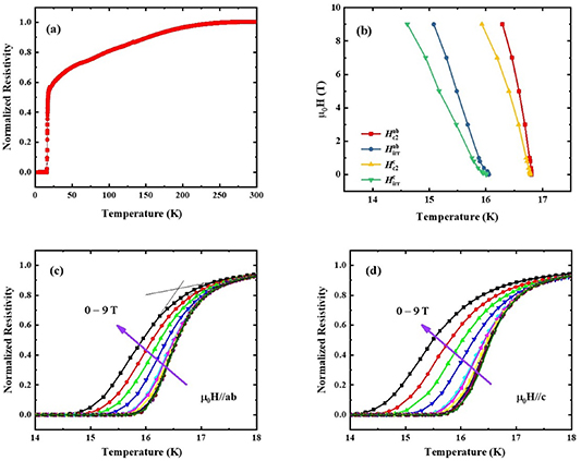
Figure 2. (a) Resistivity traces normalized by the resistivity at 300 K for the FST CCs as a function of temperature in zero magnetic field. (b) Hc2 and Hirr for major field orientations, i.e. H//ab (left) and H//c (right). (c) and (d) Resistive transitions in applied magnetic fields up to 9 T for H//ab and H//c.
Download figure:
Standard image High-resolution imageTransport measurements for the film were performed in various magnetic fields and at different temperatures, using a rotary sample holder. Figure 3(a) exhibits the values of Jc under different magnetic fields applied in the directions of H//c and H//ab at 4.2, 6, 8, 10 and 12 K. A relatively high Jc of 0.78 MA cm−2 was obtained at 4.2 K in self-field, which exceeds the value reported in [13]. Furthermore, Jc decreased to 0.35 MA cm−2 (H//ab) and 0.25 MA cm−2 (H//c) at 9 T, suggesting a small anisotropy of Jc (γ = Jc H //ab /Jc H //c = 1.4). It is noteworthy that the Jc anisotropy (defined as γJ c = Jc H //ab /Jc H //c ) is not related simply to the mass anisotropy, but shows strong both field and temperature dependence, as can be seen in figure 3(b) for the Jc anisotropy as a function of fields at temperatures of 4.2, 6, 8, 10 and 12 K. As can be seen from figure 3(b), Jc H //c is larger than Jc H //ab in fields higher than 0.4 T below 12 K and the γJ c increases monotonically with increasing field. Since Hc2 ab is larger than Hc2 c , this Jc behavior is the opposite to what is expected from the mass anisotropy [24, 25]. Interestingly, the Jc anisotropy goes into reverse at 12 K from 2 T to 9 T, that is, Jc H //ab is higher than Jc H //c , which is a typical case expected from the layered structure of FST. Accordingly, this means that the pinning mechanism changes with temperature and applied magnetic field, leading to intricate anisotropy of Jc [3]. In order to understand the progress and current development of the growth and performance of FST CCs, the FST films on various metal tapes are summarized in table 1. PLD is the most popular approach for the deposition of FST coating layer in CCs. It can be seen that various metal tapes have been used to advance the practical application of FST, including different buffer layers, such as MgO, LMO and CeO2, and different types of metal templates, such as untextured polycrystalline Hastelloy, RABiTS, unbuffered Invar 36 and stainless steel. These FST CCs have displayed promising high-field performance, as high as 0.1 MA cm−2 at 30 T, and are therefore, very attractive for applications. However, substantial effort should be devoted to further improve the fabrication process as a strong dependence of transport performance on fabrication conditions is still observed.
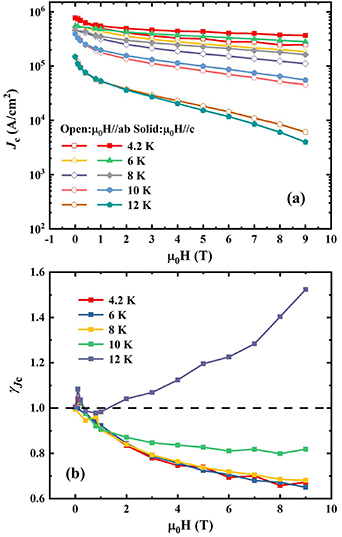
Figure 3. (a) Magnetic field dependence of critical current density (Jc) at 4.2, 6, 8, 10 and 12 K for H//ab (open symbols) and H//c (solid symbols). (b) Jc anisotropy, i.e. γJ c = Jc H //ab /Jc H //c , as a function of applied field for the 4.2–12 K range under fields from 0–9 T.
Download figure:
Standard image High-resolution imageTable 1. Summary of FST CCs by PLD. All the studies employed FeSe0.5Te0.5 superconductor.
| Template | Laser wavelength (nm) and repetition rate | Growth temperature (°C) | Thickness (nm) | Highest Tc (K) | Self-field Jc at 4.2 K | High-field Jc (MA cm−2) at 4.2 K | References |
|---|---|---|---|---|---|---|---|
| IBAD-MgO buffered metal tapes | 248 nm, 5 Hz | 300 °C–450 °C | 100 nm | 11 K | 0.2 MA cm−2 | 0.01 MA cm−2 at 25 T | [11] |
| CeO2 buffered RABiTS | 248 nm, 5 Hz | 300 °C–450 °C | 100 nm | 20 K | >1 MA cm−2 | >0.1 MA cm−2 at 30 T | [12] |
| Amorphous Al2O3 buffered stainless steel 316 | 248 nm, 5 Hz | 400 °C | 80 nm | 10 K | 1.34 × 10⁴ A cm−2 | ∼2 × 10³ A cm−2 | [39] |
| IBAD-LMO buffered metal tapes | 248 nm, 3 Hz | 400 °C | 200 nm | 16.8 K | 0.43 MA cm−2 | 0.39 MA cm−2 at 9 T | [13] |
| CeO2 buffered RABiTS | 1024 nm, 3 Hz | 320 °C | 100 nm | 18 K | 0.17 MA cm−2 | 3 × 10⁴ A cm−2 at 18 T | [16] |
| Unbuffered Invar 36 | 1024 nm, 3 Hz | 200 °C–300 °C | 200 nm | Non-superconducting | — | — | [40] |
| CeO2 buffered RABiTS | 1024 nm, 3 Hz | 220 °C–300 °C | 130 nm | 18 K | 7.9 × 10⁴ A cm−2 at 5 K | 1.3 × 10⁴ A cm−2 at 10 T | [17] |
| CeO2 buffered metal tapes | 248 nm, 3 Hz | 450 °C | 200 nm | 17 K | 0.78 MA cm−2 | 0.35 MA cm−2 at 9 T | This work |
In order to understand the anisotropic Jc behavior of the FST thin films, we quantitatively compared the angular dependence of the transport Jc(θ) measured at different temperatures and magnetic fields, as summarized in figures 4(a)–(e). Figures 4(f)–(j) illustrate the angular-dependent Jc normalized with Jc H //ab , providing the specifics of the Jc anisotropy changes. Overall, the two sets of curves are similar at 4.2 and 6 K, with Jc showing broad peaks at θ = 180° (c-axis peak), which may originate from a strong vortex pinning effect along the c-axis. Similar pinning structures play a major role in Jc(θ). As the temperature rises to 8 K and the field increases to 7 T, the minimum positioned in the neighborhood of H//ab vanishes. At 10 K, Jc peaks at θ = 90° (ab-plane peak) are not observed until the field increases to 5 T, where the ab-plane peaks are still lower than the c-axis ones. Within the field range from 3–9 T at 12 K, the ab peaks are more intense than the c-axis peaks. In conclusion, the c-axis peak becomes more pronounced as the field increases at all measured temperatures and the ab-plane peak is more prominent as the temperature increases. The variation of angular dependent Jc at different magnetic fields and temperatures arises from the evolution of pinning mechanisms.
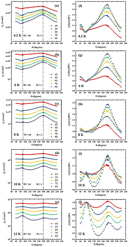
Figure 4. (a)–(e) Angular dependent Jc of the FST CC measured at 4.2, 6, 8, 10 and 12 K up to 9 T. (f)–(j) Angular dependence of Jc normalized to Jc H //ab (θ = 90º) characterized at 4.2, 6, 8, 10 and 12 K up to 9 T.
Download figure:
Standard image High-resolution imageThe scaling behavior of the pinning force density for H//ab and H//c gives us further insight into the pinning mechanism evolution occurring in the FST films on the CeO2-buffered metal tapes, as displayed in figures 5(a) and (b). The superposition of different pinning mechanisms is demonstrated by the normalized pinning force fp as a function of reduced field h, i.e. fp = hp
(1h)q
, where fp = Fp/Fp,max, h = H/Hirr. The irreversibility field Hirr is determined by the linear part of the Kramer plot: Fk
=
Jc
0.5 × H0.25 at Fk = 0 (i.e. determined by extrapolating the functional form of Jc to zero using a Kramer extrapolation [26], as described in figure 5(c)). For H//ab, the fitting parameters are p= 0.75, q= 2.66 and the peak position hmax = 0.22 (calculated by hmax = p/(p+ q)) at 10 K, p= 0.73, q= 2.15 and hmax = 0.25 at 12 K. For H//c, the fitting parameters are p= 0.69, q= 2.63 and hmax = 0.21 at 10 K, p= 0.7, q= 2.08 and hmax = 0.25 at 12 K. According to the Dew–Hughes model, p= 0.5, q= 2 and corresponding hmax = 0.2 are the typical values for pinning mechanism by surface defects such as GBs, while, p= 1, q= 2 and corresponding hmax = 0.33 are the typical values for point-defect pinning mechanism. Consequently, the values of p, q and hmax for our sample represent a combination of surface-defect and point-defect pinning mechanism. In addition, with the temperature decreasing, the peak position shifts to lower h, indicating the subdued influence of point-defect pinning and enhanced influence of surface-defect pinning. In order to distinguish the correlated and uncorrelated defects affecting the Jc(θ) properties, the anisotropic scaling approach by Blatter et al is applied to Jc(θ) data [27], i.e. Jc is scaled using an effective magnetic field Heff =  (θ)H = H(cos2
θ + γ−2 sin2
θ)1/2, where γ is the electron mass anisotropy ratio [28–30]. Figure 5(d) describes the scaling behavior of Jc versus Heff calculated with γJ
c = 1.5 at a representative temperature of 12 K. If all Jc(θ) data could collapse on a single line, this will imply a random pinning mechanism. However, it is apparent that the data in the vicinity of H//c always negatively deviate from the master curve. Furthermore, the angular range close to H//ab can be scaled up to 5 T and a similar deviation occurs at 7 and 9 T to H//c. In addition, the divergence of the Jc(θ) data close to H//ab and H//c is caused by correlated flux pinning along both major crystallographic directions.
(θ)H = H(cos2
θ + γ−2 sin2
θ)1/2, where γ is the electron mass anisotropy ratio [28–30]. Figure 5(d) describes the scaling behavior of Jc versus Heff calculated with γJ
c = 1.5 at a representative temperature of 12 K. If all Jc(θ) data could collapse on a single line, this will imply a random pinning mechanism. However, it is apparent that the data in the vicinity of H//c always negatively deviate from the master curve. Furthermore, the angular range close to H//ab can be scaled up to 5 T and a similar deviation occurs at 7 and 9 T to H//c. In addition, the divergence of the Jc(θ) data close to H//ab and H//c is caused by correlated flux pinning along both major crystallographic directions.

Figure 5. Normalized pinning force for the FST CC is reported as a function of reduced field for the 10–12 K range exhibiting the change in the dominant pinning mechanism with temperature, where the field was oriented perpendicular (a) and parallel to the c-axis (b). (c) Hirr has been determined by extrapolation using the Kramer method. (d) Scaled Jc(θ) curve as a function of Heff at a given temperature of 12 K using an appropriate anisotropy parameter of γ = 1.5.
Download figure:
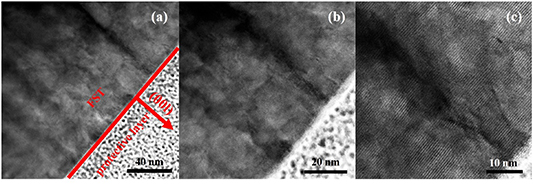
Standard image High-resolution imageTo verify the origin of strong vortex pinning along the c-axis, microstructural analysis was performed using TEM. Figures 6(a)–(c) reveal the cross-sectional TEM images of the film fabricated on CeO2 buffer layer. It is apparent that a series of vertical defects grow from the CeO2 layer along the c-axis with a little meandering, which could be attributed to GBs. The c-axis oriented defects, randomly distributed at an interval of 20–40 nm, are considered to be effective pinning centers over a wide range of field orientation, although most effective at H//c [31, 32]. It is known that GBs can be advantageous for high current carrying capabilities due to their pinning flux ability. Trommler et al reported c-axis correlated defects extending throughout the whole Ba(Fe,Co)2As2 film on Fe-buffered IBAD-MgO substrate [33]. TEM images revealed that these defects were separated by ∼20–40 nm and might be identified as GBs. Katase et al found that the co-doped Ba-122 films on IBAD/MgO showed a greater in-field Jc than a comparable film on MgO single crystal because of the c-axis correlated pinning centers, which proved GBs could contribute to flux pinning [34]. In addition, Sato et al observed high-density GBs along the c-axis in P-doped Ba-122 films on poorly aligned IBAD/MgO [35]. These vertical defects were confirmed to be effective vortex pinning centers and led to Jc peaks at H//c in Jc(θ) plots. Likewise, Iida et al ascribed the broad maximum at H//c for the P-doped Ba-122 films to GBs pinning centers, as confirmed by the pinning force analysis [36]. Hänisch et al believed the existence of high-density small-angle GBs parallel to the c-axis contributed to strong pinning in co-doped Ba-122 thin films, which resulted in a clear Jc peak at H//c [37]. These results are different to the case of an oxygen-diffused co-doped Ba-122 film on SrTiO3 (in this case, columnar oxide defects yield strong flux pinning). Lee et al and Tarantini et al both found a number of c-axis oriented columnar defects that grew from the SrTiO3 template in co-doped Ba-122 films [24, 38]. The composition of the columnar defects was proved to be BaFeO2 by electron energy-loss spectroscopy, indicating a beneficial oxygen contamination to the film growth either from the PLD chamber vacuum or from the oxygen-containing target. Since planar defects in the ab plane were not detected, the broad maximum positioned at θ= 90° (H//ab) in Jc(θ) is mainly due to the intrinsic pinning arising from coupled ab planes.
Figure 6. (a)–(c) Cross-sectional TEM images of the FST thin film grown on the IBAD-LMO metal substrates with a CeO2 buffer layer.
Download figure:
Standard image High-resolution image
4. Conclusion
In order to improve the texturing of FST CCs, an additional CeO2 buffer layer was deposited on less well-textured IBAD-LMO templates via PLD. Compared to LMO layers, the structural properties of FST films deposited on CeO2 exhibit reduced out-of-plane and in-plane misalignment, implying better crystalline quality that drives a relatively high Tc. Angular dependence of Jc measured at different temperatures and magnetic fields reveal that the dominant pinning mechanism varies with temperature and magnetic field. The larger Jc for H//c than that for H//ab, inverting the expectation of the Hc2 anisotropy, can be ascribed to the c-axis correlated flux pinning caused by GBs. Despite the higher Jc at 4.2 K in self-field, Jc //ab (4.2 K, 9 T) ∼ 0.25 MA cm−2 is lower than that of the FST film (∼0.35 MA cm−2, 4.2 K, 9 T) directly deposited on the IBAD-LMO templates [13], suggesting that there is still room for Jc improvement in CeO2-buffered FST films.
Acknowledgments
This work was supported by the National Key R&D Program of China (Grant Nos. 2018YFA0704200 and 2017YFE0129500), the National Natural Science Foundation of China (Grant Nos. 51861135311, U1832213 and 51721005), the Strategic Priority Research Program of Chinese Academy of Sciences (Grant No. XDB25000000), the International Partnership Program of Chinese Academy of Sciences (Grant No. 182111KYSB20160014) and the Key Research Program of Frontier Sciences of Chinese Academy of Sciences (Grant No. QYZDJ-SSW-JSC026).
Data availability statement
All data that support the findings of this study are included within the article (and any supplementary files).