

Abstract
YBa2Cu3O7–x (YBCO) films grown by metal-organic decomposition (MOD) are promising candidates for the production of high performance high temperature superconductors (HTS) tapes. Moreover, artificial pinning centers (APCs) introduction proved to be a powerful tool for the improvement of transport properties in YBCO films. Along with the widely employed pinning strategies, such as the introduction of secondary phases in the YBCO matrix, a less studied approach is the nanostructuring of the YBCO substrate, in order to hinder its growth and to obtain a highly defective superconductive layer. In this work, oxide nanostructures were deposited on crystalline substrates via polymer assisted deposition (PAD), a low cost, highly versatile technique, so as to create nanoparticles that could interfere with epitaxial growth of chemical YBCO films. Preliminary analyses of the superconducting films grown on BaZrO3 (BZO) and ZrO2 (ZO) nanostructures showed that the decorated templates are highly effective in straining the YBCO matrix, leading to a significant improvement in transport properties. In fact, we obtain an increase of the critical current density, at 77 K, for YBCO grown on BZO and ZO decorated substrate of the order of 3 times at 2 T and even of the order of 8 times at 5 T with respect to the YBCO grown on bare substrate. The improvement of the pinning properties can be related to the intrinsic modification of the crystal structure of YBCO film due to the presence of these nanoparticles, in agreement with transmission electron microscopy (TEM) analysis performed.
Export citation and abstract BibTeX RIS
1. Introduction
Over the past few years, many studies were dedicated to the study of the improvement of transport properties and the elucidation of the pinning phenomena occurring in YBa2Cu3O7−x (YBCO) thin films [1–7]. It is known that natural defects, such as dislocations, vacancies, low-angle grain boundaries, intergrowths or twin boundaries (TB) can act as effective pinning centers [8, 9]. However, an improvement in the current carrying capabilities of the material is required in order to fulfill the application requests [10, 11]. For this aim, several YBCO nanoengineering approaches have been investigated and successfully exploited for the introduction of controlled nanoscale defects within the superconducting matrix [12–14].
Following the idea of increasing the pinning properties of YBCO films, most of the efforts of the scientific community were focused on the introduction of artificial pinning centers (APCs) such as secondary phases inside the superconductor film with ex-situ or in-situ methodologies, such as segregated particles or columns [15–19]. In the case of films grown by chemical solution deposition (CSD), an important role in the enhancement of the pinning properties is played by the strain associated with the network of intergrowths and stacking faults emerging for the incoherent interface between secondary phases and YBCO matrix [13].
In the last few years, in addition to these widespread approaches to the introduction of APCs, a complementary method involving the modification of the substrate surfaces prior to YBCO film deposition has been explored. It was demonstrated that the decoration of the substrate surface with a variety of nanoparticles is a practical and effective alternative method to introduce additional flux pinning centers into YBCO films [14, 20–22]. The role of these nanostructures is to cause an accumulation of stress during the subsequent growth of the superconducting film [23]. This stress acts as a source of pinning for the magnetic vortices, inducing an improvement in the performance of the superconducting film.
The growth of the substrate–decorating nanostructures can be obtained through various deposition techniques such as pulsed laser deposition (PLD) and CSD [24–30], and different chemical compounds such as BaTiO3, BaZrO3, LaSrMnO6, and CeO2 have been employed for the decoration of both single crystalline and technical substrates.
First studies carried out on this type of techniques have led to unsatisfactory results, due to the fact that the density of nanoparticles (NPs) decorating the substrate was not effective on the pinning properties of YBCO films [30]. On the other hand, using the polymer assisted deposition (PAD) technique, that gave the possibility to increase the solution concentration and to easily control the solution viscosity, we successfully increased the density of nanoparticle decorating the substrate, which has led to a significant improvement of the pinning properties [31].
The purpose of this article is to study, more in detail, the pinning properties of YBCO films grown on SrTiO3 (STO) crystalline substrates decorated with BaZrO3 (BZO) and ZrO2 (ZO) using the PAD technique [31]. BZO is a commonly employed material for APC introduction and was already investigated for CSD surface decoration of LaAlO3 substrates [23]. On the other hand, ZO is known to react with YBCO precursor during growth subtracting barium from the growing film to form BZO [32]. Therefore, it could be possible to obtain YBCO on BZO nanoparticles starting from the ZO precursor solution, with all the advantages of dealing with a much simpler system.
The origin of the observed improvement of the pinning strength is investigated through a critical current density (JC) angular scaling approach. From this analysis, the highly strained nature of YBCO film, caused by the growth on the decorated substrate, is consistent with the increase of the performances. It is concluded that the substrate decoration approach with BaZrO3 and ZrO2 nanoislands can be an alternative and valid method for the increase of the pinning performances of superconducting YBCO films. In addition, from a technological viewpoint, the effectiveness of PAD method for the nanoengineering of substrates is also derived.
2. Experimental
2.1. Sample preparation
The PAD technique involves the preparation of a water based solution containing polymer, a chelating agent and the metals precursors [33]. The procedure for the PAD solution with BaZrO3 (BZO) and ZrO2 (ZO) precursors (BZO and ZO PAD solution) starts with the preparation of the individual metal-polymer aqueous solutions: Ba(NO3)2, ZrO(NO3)2 were dissolved in water together with ethylenediaminetetraacetic acid (EDTA) in a 1:1 molar ratio. Branched polyethylenimine (PEI, average Mn = 70 000) was added to reach a pH value of 5–5.5. Any unbound ion and the counter ions in the solution are removed via centrifugation in the Amicon® ultra filtration units up to constant volume of the retained fraction.
Inductively Coupled Plasma spectroscopy was used to determine the single metal precursor solutions. Then these solutions are mixed and the final concentration was adjusted to the desired value by adding ultra-pure water to (Oxide) = 0.003 M. Due to the low substrate wettability, in order to ensure homogeneous deposition, the (001) oriented STO single crystal substrates were treated at 600 °C for 2 h in O2 flow. The final polymeric solutions were spin coated on (100) SrTiO3 (STO) substrates at 5000 rpm for 60 s. The samples were then annealed at 1000 °C for 4 min in air by directly introducing the samples into the furnace, followed by quenching to room temperature. More detail on STO surface decoration has been already presented in [31, 33].
The YBCO coating solution was prepared with a low-fluorine MOD approach. Details on the preparation and thermal processing conditions are described elsewhere [34, 35]. The resulting film thickness was about 90 nm. The YBCO films analyzed in this paper on bare and on BZO or ZO decorated STO substrates were grown during the same thermal treatment using the same precursor solution, so as to avoid problems related to solution or treatment reproducibility.
2.2. Sample characterization
The x-ray diffraction (XRD) measurements, to analyze the structural properties of the films, were performed using a Rigaku Geigerflex diffractometer working with Cu-Kα radiation.
A LEO 1525 field emission high-resolution scanning electron microscopy (SEM) was used to investigate the surface morphology. Nanoparticles size and distribution were analyzed through atomic force microscopy (AFM). Analyses were performed using a Park Systems XE-150 AFM operating in non-contact mode with a pre-mounted non-contact high-resolution cantilever working at 309 MHz with a nominal tip radius below 10 nm. Images were flattened by subtracting a linear background in the fast scan direction and a quadratic background in the slow scan direction.
The TEM analysis was performed at the Electron Microscopy for Materials Science at the University of Antwerp. Plan view and cross-section transmission electron microscopy (TEM) lamellae were prepared via Focused Ion Beam (FIB). During the preparation, Pt protective layers were deposited on top of the film. The probe aberration–corrected high angular annular dark field scanning measurement transmission electron microscopy (HAADF-STEM) were carried out on an FEI Titan electron microscope operated at 300 kV.
In order to perform dc transport measurements, for the current-voltage characteristics (I–V), the films were patterned, using standard UV photolithography and wet etching to obtain 1 mm long strips with a width of 30 μm and 50 μm. The patterned samples were mounted on a sample holder and loaded in a He gas flow cryostat provided with a 7 T superconducting magnet. The sample can rotate in a wide angular range changing the magnetic field incident angle θ, with θ= 180° and θ= 90° correspond in H parallel to the YBCO c-axis and ab-plane, respectively. Critical current values as a function of the applied magnetic field or the angle value have been obtained from the I–V characteristics measurements using the 5 µV · cm−1 criterion.
3. Results and discussions
3.1. Surface decoration
Figure 1(a) shows the AFM scans of a ZO-decorated STO substrate with well-defined nanometric NPs nanometric in size, uniformly distributed over the whole substrate surface. For BZO decorated STO substrate similar features are observed.

Figure 1. (a) 1 μm × 1 μm AFM image of ZO nanoislands grown on STO, SEM images of YBCO film surface for a film deposited on bare (b) and (c) on ZO-decorated STO substrate.
Download figure:
Standard image High-resolution imageThrough the AFM image processing more quantitative analyses of nanoparticles are derived. The thus obtained NPs are characterized by typical values (averaged over several similarly processed samples) for the radius R = (17 ± 5) nm and a height h = (5 ± 1) nm for the BZO and R = (19 ± 9) nm and h = (5 ± 1) nm for the ZO, with an average particle density of approximately 200 ÷ 300 NPs μm−2 for BZO and 300 ÷ 400 NPs μm−2 for ZO [31]. More detailed characterizations of BZO and ZO NPs systems can be found in [21, 26]. The calculated density is in line with values previously reported in other works using different methods and NP systems [23, 36]. Higher values can be achieved, for example, by increasing the solution concentration or with different systems as shown in our previous work [29].
On the other hand, it has to be taken into account that an increased density, resulting in a larger coverage of the substrate surface, could ultimately be detrimental for the nucleation and epitaxial growth of the YBCO films, and then leading to poorer film quality, unless NPs radius was not progressively reduced. Both BZO and ZO NP systems studied in this work exhibit the optimal characteristics obtained so far.
3.2. Structural and morphological properties
In figure 1, SEM images show the surface morphology of YBCO grown on bare (b) and on ZO decorated STO substrate (c), respectively. For both films, the surface appears flat and compact with some outgrowths. It is worth considering that no changes on the surface morphology, due to the presence of the ZO nanoparticle, is observed. The same consideration can be done also on the film grown on BZO decorated substrate (SEM image not reported).
X-ray diffraction analysis was performed on all samples: YBCO, and YBCO on BZO and ZO decorated substrates diffraction patterns are shown in figure 2. The spectra show an epitaxial growth of the three samples and no difference with respect to the pristine YBCO sample is noticed. The calculated c-axis parameters of all the samples are in agreement with typical YBCO values reported in previous work [37], showing that the presence of BZO or ZO nanoparticle on STO surface does not affect the c-axis film growth. The full width at half maximum (FWHM) of the (005) peaks ω-scan are also reported in table 1. In addition, traces of Y2O3 are also observed. Moreover, no evidence of BZO or ZO peaks can be detected, probably because the intensity is below our experimental detection limit.
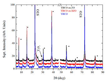
Figure 2. X-Ray diffractogram for the standard YBCO (blue line), YBCO on BZO (red line) and on ZO (black line) decorated substrate. The substrate peaks reflections are labeled with STO, and the arrows indicate the traces of Y2O3 peaks reflections.
Download figure:
Standard image High-resolution imageIn figure 3(a), the TEM cross section of the YBCO bare sample is reported. To make sure that the obtained microstructural features could be directly correlated with the transport properties, the TEM lamellae were taken from the strips used for the I–V measurement.
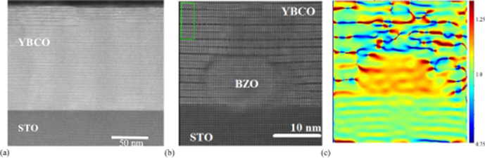
Figure 3. (a) TEM cross section of YBCO bare sample; the darker and bright zone are due to different orientation of the in-plane crystal structure of YBCO, the twin boundaries. (b) HAADF-STEM cross section of YBCO sample deposited on BZO decorated substrate, in the presence of BZO nanoparticle. The darker lines are attributed to the Cu-O chain layers along the ab direction, (c) GPA map of the interface between a BZO island and YBCO. The strain maps give the expansion or decrease of the lattice parameter in percentages within the limits ±25%. Green rectangle on the HAADF-STEM of figure 3(b) indicates the reference area.
Download figure:
Standard image High-resolution imageTable 1. Critical temperatures (TC), full width at half maximum (FWHM) of the (005) YBCO ω-scan and critical current density (JC) at 77 K and self-field of the three samples under investigation.
| Sample | TC (K) | (005) YBCO FWHM | JC(77 K, 0 T) (MA cm−2) |
|---|---|---|---|
| YBCO | 89.6 | 0.31° | 1.13 |
| YBCO on BZO decorated | 89.9 | 0.26° | 2.92 |
| YBCO on ZO decorated | 89.2 | 0.26° | 3.31 |
It is clear that the YBCO grows without major structural defects apart from the region close to surface, where stacking faults can be recognized. Furthermore, the presence of twin boundaries, visible as the succession of darker and brighter zones in the TEM image, is detected. The difference in contrast is not related to any compositional change, as confirmed by EDX analysis (data not shown), but is related to the different orientation of the YBCO lattice ([100] or [010]) [38]. The presence of twin boundaries, as observed in [39, 40], can be responsible for the anisotropic contribution to the pinning when the applied magnetic field is parallel to the c-axis.
In the case of YBCO grown on decorated substrates, the TEM image (figure 3(b)) shows that the superconducting film grows all around the BZO nanoparticle with a significant density of defects. These defects, visible as darker stripes in the YBCO matrix, can be found in the whole film thickness and are commonly referred to as stacking faults, consisting of an extra Cu-O chain between two Ba-O layers [38, 41, 42]. In these areas, the YBCO grows with a stoichiometry different from the usual one: instead of growing with the usual stoichiometry YBa2Cu3O7−x or Y123, it grows as Y2Ba4Cu8O16 or Y248.
The formation of stacking faults is probably promoted in order to release the strain that accumulates at the YBCO/BZO or YBCO/ZO interface during YBCO growth [13]. Partial dislocations at whose position all the strain is accumulated delimit the stacking fault at both edges.
The effect of strain in the YBCO lattice can be observed in the Geometric Phase Analysis (GPA) map reported in figure 3(c). The variation of the structural parameter in the c-axis direction is calculated with reference to the area of YBCO free from defects (highlighted in green in figure 3(b)). This analysis shows a high amount of strain in YBCO localized in correspondence of the edges of the stacking faults.
3.3. Superconducting properties
The critical temperatures of the all samples (TC), reported in table 1, are very similar within the limit of the experimental error, showing that the substrate decoration does not affect this parameter.
As regards transport properties, in figure 4(a), the critical current density (JC) as a function of the applied magnetic field (B = μ0H) in a configuration in which the magnetic field is parallel to the YBCO c-axis, at 77 K (filled symbols) and 65 K (empty symbols) is reported. As can be seen from figure 4(a), the values of the critical current density for the samples deposited on decorated substrates (red circles for BZO and black triangles for ZO decorated templates) are higher than pure YBCO (blue squares) in the whole field range and at both temperatures. More in detail, the values of JC at 77 K for BZO and ZO decorated samples are 0.211 MA cm−2 and 0.235 MA cm−2 at 1 T and 0.0142 MA cm−2 and 0.0175 MA cm−2 at 5 T, respectively, representing a threefold improvement compared to the 0.107 MA cm−2 at 1 T and the 0.0022 MA cm−2 at 5 T for pristine YBCO. The same trend is observed at 65 K 1 T with JC values of 0.393 MA cm−2, 0.801 MA cm−2 and 0.780 MA cm−2 for pristine YBCO, BZO decorated and ZO decorated respectively. Furthermore, the self-field values (reported in table 1) are higher for decorated samples, and also the in-field behavior is improved, with the difference between decorated and pristine samples increasing with increasing applied magnetic field. The critical current density improvement, obtained for PAD–techniques, is larger than what reported in the case of MOD Ba2YNbO6 decorated substrate [43]. This different effect can be attributed to the higher density of nanoparticles obtained in these systems.
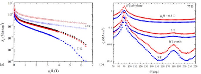
Figure 4. (a) Critical current density (JC) of YBCO film (blue square), YBCO on BZO (red circle) and YBCO on ZO-decorated substrate (black triangle) as a function of the applied magnetic field (μ0H) parallel to the c-axis measured at 77 K (filled symbol) and 65 K (empty symbol) (b). Critical current density (JC) of YBCO film (blue square) and for YBCO on BZO-decorated substrate (red circle) as function of angle (θ) at 77 K for three different applied magnetic field (0.5, 3, 5 T). θ= 90° indicates applied magnetic field parallel to the ab-plane, θ = 180° applied magnetic field parallel to the c-axis.
Download figure:
Standard image High-resolution imageFigure 5 shows the normalized pinning force f (where f = FP/FPMax, FP= JC × μ0H, and FPMax is the maximum value of the pinning force), as a function of the normalized magnetic field applied parallel to the c-axis, b (b = H/HMax, where HMax = H(Fpmax)) calculated for both 77 K and 65 K, for the three different samples. As can be seen, a perfect overlap of the curves is evident: this leads us to conclude that the mechanism responsible for pinning along the c-axis is similar in nature for both YBCO and decorated YBCO films.
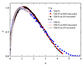
Figure 5. Normalized pinning force as a function of the normalized field at 77 K (filled symbols) and 65 K (empty symbols). Blue squares represent bare YBCO, red circle YBCO on BZO and black triangle YBCO on ZO decorated samples.
Download figure:
Standard image High-resolution imageThis improvement of the transport properties can also be analyzed through angular measurements. In figure 4(b), the critical current density is reported as a function of the angle between the magnetic field and the c-axis of the film for pure YBCO (blue squares) and for a BZO-decorated sample (red circles) at 77 K and three different applied magnetic fields, μ0H= 0.5 T, μ0H= 3 T and μ0H= 5 T. Again, the decorated sample shows improved properties in the whole angular range, for both values of the applied magnetic field. This is confirmed for all the applied magnetic field values investigated.
As shown in figure 4(b), when the magnetic field is parallel to the ab-plane, a strong increase in JC is obtained for both samples, in agreement with the YBCO structural anisotropy, with the flux lines accommodating in the insulating layers of the YBCO lattice that act as intrinsic pinning centers, as already reported in [44–46].
Under this condition, at θ = 90°, a valuable contribution is also provided by extrinsic planar defect (parallel to ab-plane) such as stacking faults or intergrowths [47–49]. Furthermore, when the magnetic field is applied close to the c-axis (θ= 180 °), a much weaker peak in JC(θ) is also observed, already visible in the curves measured at 1 T (not shown), more evident as the field increases as in the case of the curves recorded at 5 T. This second peak is attributed to other defects present along this direction, such as twin boundaries, that act as strongly correlated pinning centers [39, 40].
To better identify the contribution of isotropic and anisotropic pinning in YBCO superconducting films, JC(θ) data have been analyzed following the methodology based on the Blatter scaling function [50], recently developed and successfully applied to MOD YBCO films to sort out the anisotropic and isotropic contributions in different angular regimes [1].
This method assumes that angular JC measurements at fixed H can be plotted as JC(Heff) where Heff = H×  (γ, θ), being 2(γ, θ) = cos2(θ) + γ−2sin2(θ), with γ =
  the electron mass anisotropy of the superconductor film. In the presence of pinning centers which do not affect the electronic anisotropy in YBCO, such as point (or 0D) defects, JC(Heff) data should collapse in a single curve. Failure of this scaling can be considered as an indication of the presence of anisotropic pinning contribution.
Applying this data processing for pristine YBCO sample at 77 K with γ = 5, typical value for a pristine YBCO film [51, 52], most of the experimental points collapse on a single curve as reported in figure 6(a). The dashed line represents the JCiso(Heff) contribution obtained by fitting with the analytical expression f(H) = (1 + H/H0)−α (1−H/Hirr)β, being H0, Hirr and α and β fitting parameters. The failure of Blatter scaling indicates the presence of a dominant anisotropic pinning contribution for some θ intervals. By making the deconvolution of the JC(H× (γ, θ)), it is possible to plot the isotropic behavior JCiso(θ). The same procedure was applied to YBCO on decorated substrates assuming the same γ= 5. This is justified considering that the nature of the defects introduced by NPs, as shown by TEM analysis, does not significantly affect the intrinsic electronic mass anisotropy [53]. The as-obtained isotropic curves and the data for the YBCO and YBCO samples on BZO, at 77 K and μ0H = 0.5 T, are shown in figure 6(b), where the solid lines represent the as calculated isotropic JC(θ), JCiso(θ).

Figure 6. (a) Critical current density (JC) of YBCO film at 77 K at 0.5 (black square), 1 (green star), 3 (red circle), and 5 (blue down triangle) processed by the Blatter scaling approach and the isotropic contribution JCiso(Heff) (dashed black line). (b) Critical current density as a function of the angle for YBCO (blue square) and YBCO on BZO-decorated (red circle) at 77 K and B = 0.5 T, with the isotropic contribution obtained by the deconvolution of the JCiso(H).
Download figure:
Standard image High-resolution imageNotice that there is a large discrepancy between JCiso(θ) and experimental data in a large angular range close to ab-planes and c-axis indicating the occurrence of relevant anisotropic pinning mechanisms in those conditions. As already described, the origin of these anisotropic contributions can be mainly ascribed to the intrinsic ab-plane and twin boundaries pinning.
To quantify the anisotropic contribution of pinning in our samples, we calculated for the case of c-axis,
Where ΔJC(H||c) = JC(H||c)—JCiso(H||c), JC(H||c) is the critical current density measured along the c-axis and JCiso(H||c) is, instead, the critical current density along the c-axis, calculated from the isotropic contribution previously estimated.
In the case of ab-plane, we similarly evaluate
where ΔJC(H||ab) = JC(H||ab)—JCiso(H||ab), here JC(H||ab) is the critical current density measured along the ab-planes and JCiso(H||ab) is, instead, the critical current density along the ab-planes, calculated from the isotropic contribution.
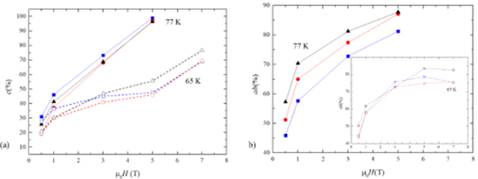
Thus, we can evaluate the trend of both ab(%) and c(%), that represent the percentage of the anisotropic contribution along both directions, for the BZO decorated, ZO decorated and pristine YBCO samples, as a function of the applied magnetic field. In detail, from figure 7(a) it is possible to notice that in the case of c(%), the three samples show similar values in the whole range of applied magnetic field at 77 K, while at 65 K the values are slightly different but still very close to each other. This means that the trend of the anisotropic contribution does not change significantly among the three samples, and that the improvement in the pinning properties along the c-axis, observed in the decorated sample, is most likely due only to an isotropic contribution. The isotropic nature of this pinning mechanism causes a shift of the JC(θ) curves measured on the decorated samples to higher values in the whole angular as observed in figure 4(b).
Figure 7. (a) Variation of the c(%) parameter as a function of the applied magnetic field at 77 K (filled symbols) and 65 K (empty symbols). (b) Trend of the ab(%)parameter as a function of the applied magnetic field at 77 K (filled symbols) and in the inset at 65 K (empty symbol). In both Figures blue squares, represent bare YBCO, red circles represent YBCO on BZO decorated and black triangles YBCO on ZO decorated.
Download figure:
Standard image High-resolution image
On the contrary, from figure 7(b), higher values for the ab(%) parameter in the samples deposited on decorated substrates are obtained at 77 K, indicating a more valuable strengthening of the anisotropic vortex pinning contribution in these samples, when the magnetic field is approaching the ab-plane. On lowering the temperature to 65 K, the effectiveness of the additional ab-plane correlated pinning centers, induced in the decorated samples, is reduced.
The origin of the different types of pinning mechanisms, most likely isotropic along c-axis and anisotropic along ab-planes, is consistent with the TEM analyses, previously reported.
The twin boundaries present in the bare YBCO sample, reported in figure 3(a), are a typical example of preferential pinning along the c-axis.
Moreover, in the case of the YBCO grow on decorated substrates, the edges of the stacking faults, highlighted in the GPA map reported in figure 3(c), act as point defects with a 3D isotropic nature. providing a contribution in the vortex pinning landscape. We think that the presence of this point defects can be the cause of the increase of the isotropic contribution in the YBCO film deposited on decorated substrate with respect to the bare YBCO, contributing to the shift to higher values of the critical current density in the whole range of fields and angles.
On the contrary, looking at the situation when the magnetic field is applied along the ab-plane, the stacking faults, showed in figure 3(b), can act as pinning centers themselves. The additional Cu-O chains could serve as preferential accommodation sites for flux lines along this direction, behaving as anisotropic pinning centers. Therefore, this effect can explain the increase in the anisotropic contribution along the ab-plane in the decorated samples at 77 K.
4. Conclusions
We have successfully grown BZO and ZO nanoislands on STO single crystal by the PAD technique. These nanoislands are homogeneously distributed on the substrate, with similar density and size in all samples.
YBCO films grown on these structures show a clear improvement of the pinning properties for all investigated field and angle values, at both 77 K and 65 K. The angular measurements were evaluated according to the Blatter et al's scaling model, in order to separate the anisotropic and isotropic contribution to the pinning properties along the ab-planes and the c-axis. The result suggests that the improvement of the transport properties observed on decorated samples along the c-axis is due to an isotropic contribution of the pinning properties, while an additional anisotropic contribution is active in decorated samples along the ab-planes. TEM analysis confirmed the presence of a high stacking fault density in decorated samples mostly in the regions surrounding the BZO and ZO nanoparticles, that can act as additional pinning source when the applied magnetic field is parallel to the ab-planes.
These results indicate that PAD is a suitable technique for substrate decoration and that substrate decoration is a concrete alternative strategy for the introduction of artificial pinning centers.
Further investigations of the critical current density properties at lower temperatures need to be carried out in order to get a more complete assessment of the potentiality of this approach.
Acknowledgments
This work has been carried out within the framework of the EUROfusion Consortium and has received funding from the Euratom research and training program 2014–2018 and 2019–2020 under grant agreement No 633053. The views and opinions expressed herein do not necessarily reflect those of the European Commission.