
Abstract
Gaining engineering critical current density (Je) in high-temperature superconducting (HTS) coated conductors based on double-disordered YBCO for operation at high fields is one of the key requirements in upcoming magnet/accelerator projects. Currently, the development of a tape with advanced Je-s is performed based on an alternating beam-assisted deposition–pulsed laser deposition (ABAD–PLD) manufacturing route. An obvious way to improve Je-s is to reduce substrate thickness. A 40% Je increase is expected owing to the thickness reduction from 100 to 50 μm. Nevertheless, the reduction of substrate thickness in case of the applied processing technology that employs relatively thick (2–3 μm) yttria-stabilized zirconia buffer layers leads to the manifestation of considerable strain in the tape resulting in strong tape bowing. Advanced processing routes have been developed to suppress this effect. The highest engineering current density was recorded at well above 1000 A mm−2 under an ultra-high field of 18 T at 4.2 K, B//c. Influence of tape bowing and the impact of longitudinal defects are studied via V–I measurements at 77 K and a moderate magnetic field with intrinsic edge gradients. Potential for further gaining of Je was found employing mechanisms of (i) film nucleation from lateral flows that provide material transfer during the PLD process. Further steps include suppressing the instability of instantaneous temperature via quasi-adiabatic pulsed heating of the growing HTS film via (ii) control of laser plume energy, and (iii) energy release during film condensation (condensation enthalpy). These effects disturb the instantaneous temperature of the growing HTS layer, which exhibits very limited capability of heat transfer. Temperature pulses reaching 30–40 K were evaluated via heat transfer modeling. Stabilization of the level of pulsed temperature during layer growth is anticipated to result in a further increase in Je.
Export citation and abstract BibTeX RIS

Content from this work may be used under the terms of the Creative Commons Attribution 3.0 licence. Any further distribution of this work must maintain attribution to the author(s) and the title of the work, journal citation and DOI.
1. Introduction
High-temperature superconducting (HTS) coated tapes initially aimed at 'high-temperature' applications (e.g. at 77 K) acquired an important additional role as a low-temperature superconductors due to their extraordinary high engineering current density, Je, remaining in ultra-high fields, well above 20 T. Intensive efforts have been made to establish a reliable technology for fabricating long and high-Je tapes for high and ultra-high fields at Bruker HTS, Fujikura, SuperPower/Furukawa, etc [1–3].
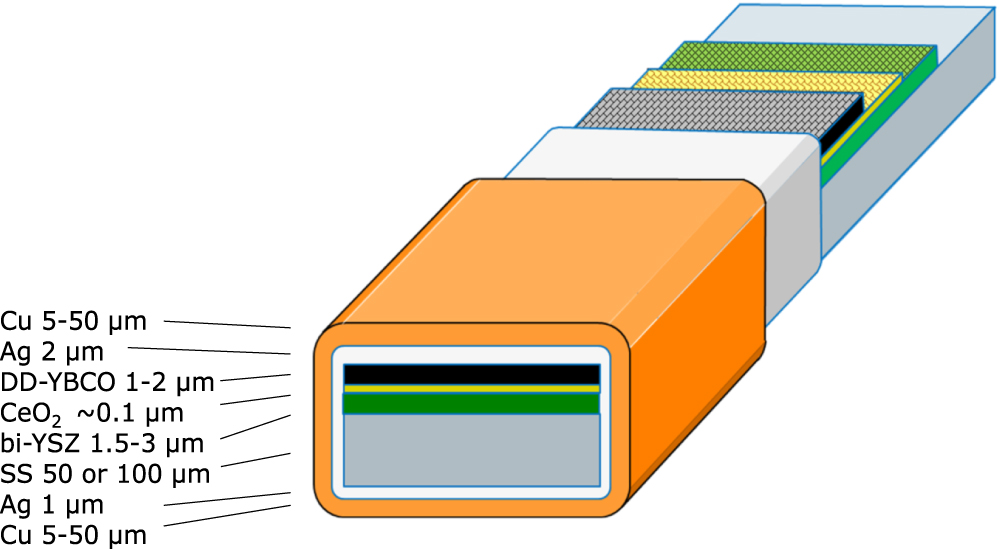
The Bruker HTS technological chain was established and fine-tuned for a 100 μm thick substrate. This relatively high thickness enables favorable mechanical properties that are important for ultra-high field magnets. Despite their excellent critical currents (>1000 A cm−1 width at 18 T, B//c, 4.2 K), the thick Bruker tapes yielded high but not the highest level of engineering current density (600–800 A mm−2 at the same conditions [3]). Numerous projects, particularly by CERN within the ARIES project [4, 5], have been initiated to increase Je for our processing route. The reduction of substrate thickness in the employed tape design (as shown in figure 1 to achieve this goal seems to be the simplest. In reality, with a 50 μm thick substrate, major core steps in the employed processing route, such as alternating beam-assisted deposition (ABAD) [6] and pulsed laser deposition (PLD) [3, 7, 8] must be re-tuned because of a substantial variation of mechanical and thermal parameters of a thin substrate.

Figure 1. Cross-sectional design of HTS coated tape manufactured at Bruker HTS GmbH with length of 600 m. SS denotes CrNi stainless steel (or Hastelloy) used as a substrate material, bi-YSZ: bi-axially textured yttria-stabilized zirconia buffer layer deposited via ABAD, CeO: CeO2 buffer cap layer deposited via PLD. DD-YBCO: double disordered superconducting layer [3] based on YBa2Cu3O7−δ deposited via PLD. Ag: silver protection layer deposited by thermal vacuum evaporation, Cu: copper layer deposited via galvanic plating.
Download figure:
Standard image High-resolution imageThis work was aimed at (i) exploring recent technological progress in tape production, (ii) finding and analyzing new, advanced conditions for processing HTS-coated tapes based on thin substrates, and (iii) determining the potential for further gaining of Je by using recently established physical mechanisms and features of a deposition process.
2. Processing platform
The HTS-coated tapes are based on CrNi stainless steel (or Hastelloy) with thickness of 100 μm ('thick' substrates) and 50 μm ('thin' substrates) and tape widths of 4 or 12 mm. The tapes were electro-polished, or alternatively mechanically polished and finally ultrasonically cleaned. ABAD [6] was employed for deposition of a bi-axially textured yttria-stabilized zirconia (YSZ) buffer layer, typically 2–3 μm thick. PLD is based on a drum-supported tape with equilibrium heating of the tape via hot wall reactor positioned in the deposition zone [3, 8]. Further details of PLD including a discussion of mechanisms determined growth of double disordered (DD) superconducting layers [3] based on YBa2Cu3O7−δ can be found in [8]. The final steps of tape manufacture include enveloping of the tape with a 1–2 μm thick silver layer deposited via thermal vacuum evaporation and metallization; the final steps of tape fabrication are described in [7, 8].
3. Tape performance
3.1. Critical current and engineering current density
In-field performance of DD-YBCO-based tapes with different substrate thicknesses is shown in figure 2, which plots the critical current versus flux density for a set of samples (end pieces of long tapes). The areas viewed in figure 2 as high-field (HF) and ultra-high-field (UHF) tapes are defined via a simple condition, Ic,UHF(B) > 2020·B−0.73 , that allows to distinguish the DD-YBCO tapes of HF or UHF class. Such definition is possible because the Ic(B)-dependence is well defined by α-law [1] in the wide field range. The tapes with lower Ic correspond to HF tapes because even with moderate current level they are able to carry sufficiently high currents (>300 A) in 4–10 T -range. UHF tapes must transport high currents in 10–31 T range. Thus, their Ic level in wide field range must be higher.

Figure 2. Field dependence of critical current measured in a set of end-pieces of 500–600 m long tapes at 4.2 K, B//c. Measurements were performed at NHMFL by Abraimov, Bradford, Jaroszynski, and Larbalestier. Red star indicates a specific point at 18 T, where Ic = 454 A and highest value of Je = 1261 A mm−2 was achieved. Substrate thicknesses are indicated in the list of samples.
Download figure:
Standard image High-resolution imageThere is a scattering of Ic-s, which, nevertheless is not degrading in tapes with thinner substrates. In general, the overall scattering of in-field Ic per cm-width, as shown in figure 3, for routinely produced tapes indicates technological progress regarding increase of reproducibility and yield.
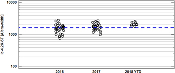
Figure 3. Actual Ic per cm (width) in-field measurements of long HTS tapes.
Download figure:
Standard image High-resolution imageIn the 4 mm wide tape, Q021-18N1, based on a 50 μm thick substrate, the highest Ic value observed was 454 A at 18 T, B//c, and 4.2 K (the red star in figure 2). Considering the Cu plating of 2 × 20 μm, the total tape thickness is 90 μm, which is 50 μm thinner than that of our thick substrate tapes. This results in a champion level Je = 1261 A mm−2 (that nevertheless should not be interpreted as a standard tape quality, more a level that is potentially achievable). However, we can expect an increase in Je because of the reduction in the tape thickness. The thickness reduction factor of 1.56 (140 μm/90 μm) leads to an increase of Je from 800 to 1244 A mm−2, where 800 A mm−2 represents a high level Je for a 100 μm substrate of HTS-coated tapes [3]. This is in good agreement with the observed value of 1261 A mm−2 and indicates the potential to gain even higher Je values because the Je of the tapes with 100 μm thick substrates may exceed the 800 A mm−2 [3] mentioned earlier.
Figures 4(a) and (b) show the reduction of Ic in the course of tape bending. A new device with a variable bending radius enabled measurements without dismounting the tape sample. The critical bending radius for the 50 μm case corresponded to Rcr = 4.5 mm. This value is half that of Rcr = 8.9 mm observed at 100 μm (see figure 4(b)).

Figure 4. (a) Device employed for bending tests and (b) Ic versus bending radius measured for a 12 mm wide tape based on 50 and 100 μm thick substrates.; the tapes are enveloped with a 1.5 μm thick silver layer. (c) Effect of bowing in 12 mm wide tapes.
Download figure:
Standard image High-resolution image3.2. Transverse bowing
A characteristic feature of the ABAD–YSZ buffered tapes is a bowing that originates from compressive stress occurring mainly during the growth of the buffer layer. This is a well-known effect caused by atomic peening [9] occurring in the course of the sputter-based ABAD employed in our processing route. Furthermore, a significant degree of bowing is retained by the tapes after deposition of all layers and intermediate annealing. This bowing effect can be seen in figure 4(c), where a cross-section of a 12 mm wide tape is depicted (left tape). The bowing height may exceed several millimeters depending on the thicknesses of the buffer layer and substrate. Such tapes show inhomogeneity of the in-plane texture, which results in an inhomogeneous Ic over the tape length. This can be seen in figure 2 for samples Q020-N1 and Q020-N2 which represent different parts of the same tape. The difference in Ic at 20 T corresponds to ∼6%. In some cases, this difference may exceed 10%.
We found that that this effect can be suppressed by the adjustment of the deposition parameters and introduction of additional layers. As a result, the tape has a significantly lower bowing height as is shown in the right-side tape in figure 4(c). Nevertheless, some residual bowing should be considered during tape processing, especially for thin substrates with a width of 12 mm.
3.3. Impact of longitudinal defects
Any technology based on reel-to-reel tape translation [10, 11] may expect intermittent longitudinal defects, e.g. scratches, especially in bowed tapes. In this work, we simulated such defects by scratching the finished tape (without the Cu layer) by using a hard material tool.
We measured the impact of an artificially introduced, 2 cm long surface scratch on the critical current at 77 K. The total dimension of the sample was 12 cm × 0.4 cm; the voltage contacts were separated by a distance of 3 cm and the initial critical current was 38.5 A (curve 1 in figure 5).
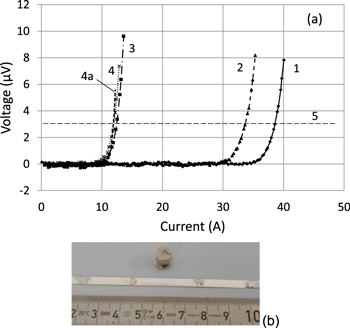
Figure 5. (a) V–I curves observed at critical current measurements in non-treated sample at SF (1) and 0.4 T (3) at field oriented perpendicularly to the tape and localized within ∼5 mm long area between voltage probes. Mechanically treated (scratched) tape exhibits a ∼13% deterioration of critical current at SF (2) and 4% deterioration (4) when the field is applied. V–I curve (4a) results from modeling via equation (1). The dashed line (5) indicates transition criterion. (b) View of investigated sample.
Download figure:
Standard image High-resolution imageWe used the criterion of 1 μV cm−1 voltage drop between contacts (i.e. 3 μV at 3 cm distance) to define Ic. With a scratch, the critical current (curve 2) degraded to 33.6 A, i.e. by ∼13%. This degree of deterioration also seems to be typical of the slitting of the manufactured tapes.
We compared Ic degradation due to the scratch in a field produced in the gap between 2 disc-like permanent magnets creating a flux density B ∼ 0.4 T. In this particular field applied perpendicular to the tape, Ic is reduced to 12.4 A, i.e. by a factor of ∼3 compared to the initial tape. In scratched tape, Ic reduces to 11.8 A in the field, yielding a difference of 5%. In contrast to the 13% reduction, this minor influence of a scratch at 0.4 T seems surprising. Here, we must consider the 'zooming' effect, which is pronounced in the local magnetic field. Owing to the drastic suppression of the in-field critical current, voltage drop Utot in the measured tape is mainly determined by the in-field tape area. This follows from the n-law, which in the considered case of the coordinate-dependent field, may be generalized as

where the in-field area with the lowest Ic-s determines the fraction of the integrand. Here, Ucr is a criterion used for defining Ic, L is the distance between voltage probe contacts, B(x) is a linear distribution of flux density in the longitudinal direction of the tape, and n(B(x)) is a coordinate-dependent power value used instead of n-values employed in the constant field case. The approximation via (1) (figure 5(a), curve 4a) sufficiently agrees with that obtained through the experiment, similar to the approximation suggested in [12]. However, the approximation predicts a 7% reduction of Ic instead of the observed 5%. This suggests that further features of tape behavior within field gradients should be considered. Nevertheless, the dominating influence of defects remaining in the field was confirmed.
4. Potential for further Je gain and discussion
4.1. Impact of lateral flows in PLD
In [3], we showed that the distribution of the deposited material that originates from the stationary (i.e. fixed) laser plume is extremely wide, considerably exceeding the diameter of the laser plume. Figure 6 shows the fragment of the interferogram (with fringes of equal thickness) of the pulsed-laser-deposited DD-YBCO on the Al-foil substrate attached to the PLD drum; the deposition was at 25 °C–35 °C. Despite the drum curvature (100 mm−1), fringes of equal thickness on the flattened foil are circular (not elliptical as expected). The layer-thickness distribution derived from the interferogram is depicted in figures 7 and 8. The 2D distribution exhibits a Gaussian-like shape with an eroded peak caused by self-etching [3]. The radius of the distribution is rather large. For deposition from a moderately sized plume where the radius exceeds 50 mm and for a large sized plume, visible fringes indicating a layer thicknesses of 100 nm were observed at a radius of >100 mm. The shape of the distribution can be explained by the lateral flows (LFL) and is essentially axial-symmetric despite the drum curvature, confirming that LFL follows the drum surface, similar to elastic flow for Mach number M > 5 [13–15]. This similarity remains valid in the case that LFL is bypassing an obstacle on the surface: we observed thickness distributions that indicate characteristic 'jumps' of the ultrasonic flow. A rough estimation of the speed of the initial flow yielded ∼5 km s−1 (for a target-to-substrate distance of ∼5 cm and plasma propagation time of <10 μs). Thus, M ∼ 15 implies that the process is within the high hypersonic range.
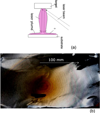
Figure 6. (a) Schematic view of plume propagation that caused by lateral flows at substrate interface, and interference picture (b) caused by thickness distribution of DD-YBCO layer deposited at room temperature onto Al foil attached to the drum of PLD set-up. Despite the drum curvature (100 mm−1) the fringes of equal thickness at flattened foil are circular (not elliptical). Corresponding thickness distribution is shown in figure 8.
Download figure:
Standard image High-resolution image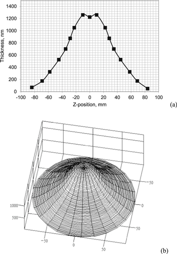
Figure 7. Thickness distribution provided via lateral flow and etching effect [3] (in the cone center). A plume is caused by a minimal beam energy. The maximal thickness exceeds 1000 nm; 4000 ablation pulses are used for deposition. Shape of distribution is practically axial-symmetric despite the drum curvature. This confirms that LFL follows the drum surface similarly to elastic flow with M > 5.
Download figure:
Standard image High-resolution imageDeposition in plume-scan mode at standard deposition temperature confirmed this wide distribution remains under actual process conditions [3]. In figure 8, we plotted this distribution together with the critical currents measured at thickness slope area (i.e. over −20 mm < Z < 30 mm): they exhibit relatively good agreement.
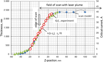
Figure 8. Thickness distribution of DD-YBCO layer deposited at linearly scanned substrate with laser plume within z from 0 to 150 mm (triangles). Distribution modeled via Gaussian approximation (rhombs) is taken from [3]. Critical current distribution measured at 77 K, SF (circles) related to 4 mm wide tape.
Download figure:
Standard image High-resolution imageThe observed wide distribution of layer thickness implies that nucleation of DD-YBCO starts far away from the scan area of the laser plume. Considering that film nucleation starts at the nanometer thickness range, the distance from the center of the laser plume may be considerably higher than the radii shown in figures 6 and 7. This offers a good opportunity to independently control layer nucleation via creating different conditions (e.g. temperature and oxygen pressure) in the nucleation zone. As such, the DD-nanostructure and as a result the Je performance may be further improved.
4.2. Instantaneous temperature at YBCO surface
The substrate temperature varies rapidly for any PLD process [16]. By using a drum-based tape support with fast drum rotation in the tubular heating zone, temperature oscillations are basically suppressed but not completely eliminated [10]. Especially, the amplitude of residual temperature oscillations is much more pronounced in the case of thin substrates (50 μm), where this amplitude may exceed 5 °C with a transient time of tens of milliseconds. This seems to be tolerable for PLD processing, as HTS layers with the highest Je were prepared in this way.
Nevertheless, the process window for substrate temperature is not very wide, possibly less than 10 °C, especially in the case of DD-YBCO.
Recently, we found that there is another, even more powerful source for temperature perturbation. This source is the energy release of ions impinging upon the growth surface of the DD-YBCO layer. The key factor that motivated us to analyze this case was that the thermal conductivity of the YBCO layer is extremely poor in the c direction, i.e. perpendicular to the growth direction.
Owing to the short lifetime of the laser plume, the integrated incident ion energy of ∼0.05 J cm−2 was delivered to the interface within 5–10 μs. Conditions for thermal accumulation and release for the given case are schematically shown in figure 9. Owing to the low thermal conductivity of ∼1 W Km−1 at T > 300 K [17, 18], YBCO represents a 'bottleneck' for heat release in the normal direction to the substrate that, in this case, together with the buffer layer plays the role of a heat reservoir. The alternative route for heat release via IR emission, which increases with increasing temperature, was shown to be negligible in comparison with heat conduction.
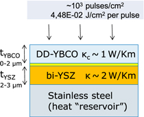
Figure 9. Conditions for heat accumulation and release in YBCO layer with variable thickness. This layer in coupled through YSZ buffer layer to stainless steel substrate which plays a role of 'heat reservoir' in given process.
Download figure:
Standard image High-resolution imageThe heating–cooling kinetics evaluated for a heating pulse with a 10 μs duration are shown in figure 10 for an arbitrary offset temperature of 781 °C, used here as an example. We assumed that energy flow originating from the laser plume is constant during the 10 μs pulse (see curve 1 in figure 10). Power delivered to the growth interface during the pulse was estimated as 4.5 kW cm−2. The specific heat capacity of YBa2Cu3O7−δ was assumed at 0.8424 J g−1 K−1 and the layer density was 5.985 g cm−3 [19].
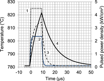
Figure 10. Heating–cooling kinetics evaluated for heating pulse with 10 μs duration is revealed for arbitrary offset temperature of 781°C. Curve 1 indicates pulsed power density versus time. Fast heating and temperature release takes place at the beginning of layer growth (curve 2). At the mid of layer growth (curve 3), temperature kinetics exhibits a slower temperature saturation and release. At the growth end, when the full thickness is reached, the heating/cooling kinetics slows considerably exhibiting a suppressed saturation (curve 4).
Download figure:
Standard image High-resolution imageAt the beginning of YBCO growth (see curve 2 in figure 10), when the layer thickness is 0.5 μm, the instantaneous temperature at the YBCO surface increased quickly by ∼22 °C and decreased rapidly after the heat pulse ended. This could have been a result of two factors: increasing heat capacity of the layer and increasing heat resistance with growing thickness.
At an intermediate thickness of 0.75 μm, the maximal increase of the instantaneous temperature exceeded 33 °C. The kinetics of temperature saturation and temperature release become considerably slower (curve 3 in figure 10).
At the end of growth when the layer thickness is about 1.5 μm, the increase of temperature becomes more linear and does not reach saturation (curve 4 in figure 10). After the pulse a temperature increase above 42 °C occurs, and the YBCO temperature decays much more slowly, taking tens of μs, because (i) much more energy is stored in a thicker layer, and (ii) of increased heat resistance introduced by the HTS layer.
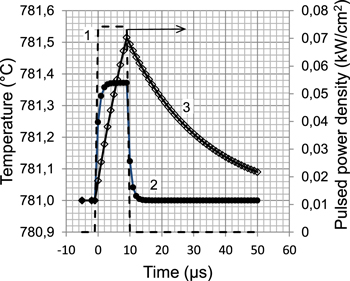
Another possible reason for the instability of the instantaneous temperature of the YBCO interface is the impact of energy released during material condensation caused by the deposition pulse. Because of the short (<10−5 s) migration time of adatoms on the surface of the growing layer [20, 21] a rapid condensation should take place. Calculation of the energy released via condensation enthalpy is shown in figure 11 that similarly to figure 10 evaluates the kinetics of instantaneous temperature assuming a 10 μs long PLD 'condensation' pulse.
Figure 11. Instantaneous temperature pulse caused by release of condensation energy (enthalpy) during deposition pulse. Heating pulse-cooling kinetics evaluated for a heating pulse with 10 μs duration (curve 1). Arbitrary offset temperature of 781°C is used. Curve 1—power density delivered via condensation energy. Curves 2 and 3—temperature kinetics at the beginning and the end of the YBCO layer growth, respectively.
Download figure:
Standard image High-resolution image
The vaporization enthalpy of the DD-YBCO composition was evaluated and employed in modeling of the condensation process in which the energy should be released. The energy was evaluated as about 5% of the energy transferred by ions. However, the pulse temperature was significantly lower, determined by only 2% of the energy triggered pulse, due to LFL which distributes the energy over a large substrate area. Because of the pulsed nature of PLD, energy and temperature effects occur as a sequence of short pulses [3, 22]. Temperature pulses originating from condensation enthalpy should be added to the temperature pulses caused by 'condensation' of ion energy.
Thus, the evaluated pulses of the instantaneous temperature are shown to be rather high, exceeding a tolerance for deposition temperature by a factor of 4 at least. Because the temperature pulses are dependent on layer thickness, one may employ a compensation of the perturbation effect via decrease of the background substrate temperature during deposition process. This may be employed as a tool for improvement of DD-YBCO growth kinetics and, finally, increase of critical current density.
4.3. Expected improvement of critical current
The DD-layer growth employing the PLD with LFLs has already been used in the processing of ultra-high field tapes, which yield a very high engineering current density at a high magnetic field (see figure 2). Nevertheless, this process, in combination with compensation of the instantaneous temperature of YBCO surface, has not yet been sufficiently developed.
The first steps in this direction resulted in the improvement of the critical current density Jc by at least 10% (at 4.2 K, 5 T, B//c). As shown in table 1 representing two tapes, tape Q047C is deposited without variation in deposition temperature Tdep, and tape Q068V is deposited under 17 K higher nucleation temperature Tn. In the case of tape Q068V, the nucleation occurred inside a preheating area of the tubular heater used in PLD [3]. The material for this nucleation (which corresponds to ∼10% of the layer thickness) was delivered by the lateral flows (LFLs). The improvement of Jc and Ic in this case is reproducible enough to confirm the presence of the gaining effect. This can be observed despite insufficient amplitude of temperature variation (17 K instead of 35 K). Moreover, the temperature during the major part of layer deposition remained almost constant, while a further variation was needed according to new results (figure 10). Following the 'sensitivity' of Ic to the deposition temperature, a 20%–30% Ic improvement should be reachable when the foreseen temperature variation is introduced during DD-YBCO growth. In our drum technology, with a one-directional path of the tape through the deposition zone, the implementation of such a variation could be possible in future studies.
Table 1. Gain of critical current and current density in the tape deposited with increased temperature during nucleation of DD-YBCO layer.
| Tape # | Tn–Tdep | Jc (4.2 K, 5 T, B//c) | Jc, Ic gain |
|---|---|---|---|
| K | MA cm−2 | % | |
| Q047C | 0 | 14 | 0 |
| Q068V | 17 | 16 | 15% |
5. Conclusion
High performance DD-YBCO coated conductors of reduced substrate thickness (from 100 to 50 μm) of 4 and 12 mm width, are routinely processed in lengths up to 600 and 100 m, respectively. A champion level of engineering current density of well above 1000 A mm−2 at 18 T, B//c, 4.2 K was observed in DD YBCO coated tape based on 50 μm thick substrate. We developed and implemented a means for suppressing tape bowing that is especially pronounced in thin tapes. The impact of longitudinal defects (scratches) on the U–I dependencies in the magnetic field exhibits a nontrivial effect, where the influence of partial damage to the tape is reduced in a gradient field area.
Potential for further gain of Je is shown via (i) independent control of nucleation temperature: that may be achieved by activation of lateral flows responsible for PLD nucleation, and (ii) compensation of instantaneous temperature instability (of 20 °C–40 °C) introduced by impinging ions from the laser plume. The minor impact of condensation energy (enthalpy) released during pulsed crystallization of YBCO is shown. The experimental results confirmed, at least partly, our expectations on the 20%–30% gain of the critical current via temperature variation during layer growth under lateral flows. The implementation of this art of deposition will be accomplished in future studies.
Acknowledgments
We acknowledge support of this work by the ARIES EC Project, Grant Agreement no. 730871, and the EASITrain Project: European Union's H2020 Framework Programme Grant Agreement no. 764879.g. 10.
The authors would like to acknowledge the support of D Abraimov, G Bradford, J Jaroszynski, and D C Larbalestier at NHMFL/FSU, Tallahassee, for high-field measurements.