
Abstract
We propose and demonstrate a novel method to enhance vibration harvesting based on surge-induced synchronized switch harvesting on inductor (S3HI). S3HI allows harvesting of a large amount of energy even from low-amplitude vibrations by inducing a surge voltage during the voltage inversion of a synchronized switch harvesting on inductor (SSHI). The surge voltage and the voltage amplification from the conventional voltage inversion improve energy harvesting. S3HI modifies SSHI by both rewiring the circuit without adding components and using a novel switching pattern for voltage inversion, thus maintaining the simplicity of SSHI. We propose a novel switching strategy and circuit topology and analyze six methods that constitute the S3HI family, which includes traditional S3HI and high-frequency S3HI. We demonstrate that the six methods suitably harvest energy even from low-amplitude vibrations. Nevertheless, the harvestable energy per vibration cycle depends on the switching pattern and storage-capacitor voltage. The use of the proposed switching strategy, which allows energy harvesting before energy-dissipative voltage inversion, substantially increases the harvestable energy per vibration cycle. In the typical case considered in this study, the said increase is on the order of 11%–31% and 15%–450% compared to the traditional and existing high-frequency S3HI methods, respectively, depending on the storage-capacitor voltage. Additionally, the proposed circuit can be used as a traditional circuit. It could be considered a promising alternative to S3HI methods owing to its potential auto-reboot capability, which is not found in traditional S3HI circuit.
Export citation and abstract BibTeX RIS

Original content from this work may be used under the terms of the Creative Commons Attribution 4.0 license. Any further distribution of this work must maintain attribution to the author(s) and the title of the work, journal citation and DOI.
1. Introduction
Technologies to generate electric power from an ambient source have attracted increasing interest for over a decade, with the aim of enabling applications such as sensor networks, environment monitoring in remote locations, and health monitoring of structures in inaccessible areas. Such a technology may replace batteries and power lines to achieve standalone systems that require low or no maintenance. Ambient energy sources include sunlight, temperature gradient, wind, tides, and vibration. Vibration-energy harvesting using piezoelectric materials is being actively studied, given its high efficiency. The standard method for energy harvesting involves connecting a full-bridge rectifier (FBR) and a storage capacitor to a piezoelectric element attached to a vibrating structure, but the harvesting performance is low. Ottman et al [1, 2] integrated a DC/DC converter into this simple circuit and controlled the converter for maximum power harvesting. Lefeuvre et al [3] proposed synchronous electric charge extraction (SECE) for harvesting the energy from a piezoelectric element into a storage capacitor by using an inductor and a switch. Based on a semi-passive vibration control method called synchronized switch damping on inductor [4], Guyomar et al [5] proposed a nonlinear harvesting method called synchronized switch harvesting on inductor (SSHI). In SSHI, the polarity of the voltage across the piezoelectric element is inverted by switching an inductive shunt circuit in synchrony with the structure vibration. Hence, SSHI increases the absolute value of the voltage across the piezoelectric element for energy harvesting. This method attracted research attention owing to its simplicity and high performance, driving various developments on vibration-energy harvesting using piezoelectric elements.
Lefeuvre et al [6] studied a series SSHI method with the piezoelectric element series-connected to an inductor. Lallart et al [7] proposed a hybrid SSHI method to accommodate a wider range of load impedances. Numerous strategies were subsequently developed, including synchronized switching and discharging to a storage capacitor through an inductor [8], double synchronized switch harvesting [9], enhanced synchronized switch harvesting (ESSE) [10], and energy injection [11]. Guyomar and Lallart [12] reviewed and evaluated some of these approaches. To increase the frequency range of the exciting force, nonlinear mechanical structures have been proposed, as reviewed by Tran et al [13]. Recently, researches to improve and extend SECE and SSHI have been actively conducted. Lallert et al [14] proposed synchronous inversion and charge extraction (SICE). Du and Seshia [15] proposed a technique called synchronized switch harvesting on capacitors, which can reduce the volume of circuits drastically. Badr et al [16] proposed a parallel-type SSHI method using a negative voltage converter. As mentioned above, several developments have successfully increased the available power for harvesting from vibration generators under various conditions.
Various applications of vibration-energy harvesters present intermittent bursty consumption of large amounts of energy. For example, health-monitoring devices transmit data intermittently and consume more energy during communication. The amplitude of vibration may vary depending on the environmental conditions. Even when the vibration amplitude is reduced, the monitoring devices need to communicate at the same time intervals. For such applications, a higher energy-harvesting rate (i.e. harvested energy per period of vibration cycle) and higher upper limit of storable energy from low-amplitude vibrations are desired. This is equivalent to maintaining a high energy-harvesting rate over a wide range of storage-capacitor voltages covering higher voltage, even when the vibration amplitude is small. However, in the classical SSHI, the storage capacitor is charged only when the voltage across the piezoelectric device exceeds that of the storage capacitor plus the forward voltage drop (FVD) of the diodes in the bridge rectifier, thus limiting energy storage, especially under small-amplitude vibrations.
Makihara et al [17] proposed a switching strategy for SSHI considering vibration suppression, and Yoshimizu et al [18] proposed its adaptive version to increase the upper limit of storable energy by waiting for vibration amplitude recovery from the depressed status by energy harvesting—they achieved successful results. However, in principle, the amount of gain is limited to the recovery of loss.
Remarkably, Kwon et al [19] proposed charging the storage capacitor even under a small vibration amplitude, a high-voltage charge of the storage capacitor, and a non-negligible FVD. They called this method surge-inducing synchronized switch harvesting (S3HI). In S3HI, a surge voltage is generated by turning the switch off while current still flows through the inductor at the end of SSHI voltage inversion. By exploiting this surge voltage, more energy can be stored compared with the conventional SSHI. Moreover, in the high-frequency S3HI method, a higher harvesting rate is achievable over time if the switch is turned off several times during voltage inversion [20]. The S3HI methods are suitable for systems that intermittently demand high consumption.
The objective of this study is to further enhance the energy harvesting rate and upper limit of storable energy of the S3HI method, even under small-amplitude vibrations with a non-negligible FVD. In this study, we considered a conventional and a high-frequency S3HI as two methods in the S3HI family. In addition, we aimed to develop and demonstrate new methods from the S3HI family to further increase the harvesting performance. Consequently, we propose a switching strategy to harvest energy at the beginning of voltage inversion, unlike conventional and high-frequency S3HI. As voltage inversion dissipates energy in the piezoelectric element, the proposed method may enhance the efficiency and harvesting rate. In addition, we propose and evaluate a circuit topology for energy harvesting. Then, we thoroughly characterize the methods in the S3HI family. Specifically, we theoretically and experimentally analyze six combinations of two circuits (the proposed circuit and that used in [19] and [20]) and three switching patterns (the proposed pattern and those in [19] and [20]) considering various scenarios.
In this study, the amplitude of mechanical vibrations remains constant, irrespective of the energy-harvesting action performed. Therefore, this study is limited to the case involving a weak coupling between the mechanical and electrical systems. Cases involving strong coupling are to be taken up in a future study. Further, the interaction between the exiting forces and mechanical vibrations (such as resonance) is out of the scope of this study.
The remainder of this paper is organized as follows. In section 2, we describe the conventional SSHI method. Section 3 presents the operation of each method in the S3HI family, including the method combining the proposed switching strategy and circuit topology. In addition, we approximate algebraic equations to estimate the performances of the methods, only omitting lengthy derivations. In section 4, we report numerical simulations and their results, which are compared with approximate solutions to verify their consistency. In section 5, we report experiments and their results, which are compared with the simulation results. In section 6, the performance and characteristics of each method in the S3HI family for various scenarios are investigated by using the previously verified numerical simulations. Finally, we draw conclusions in section 7.
2. Conventional SSHI
We describe the typical SSHI behavior and approximate the harvesting performance by obtaining the harvesting rate. Figure 1 shows the system outline for the SSHI method. The circuit consists of a piezoelectric element attached to the vibrating structure, an inductor L, a switch, and a storage capacitor  that is connected via an FBR. The vibrating structure is modeled by a mass and a spring. The piezoelectric element is modeled by a capacitance
  and a voltage generator with voltage
  .
.  denotes the capacitance of the piezoelectric element when the displacement of the mass shown in figure 1 is restricted; and
  denotes the open-circuit voltage of the piezoelectric element. The mass displacement is given by
  , where
  is the constant vibration amplitude and
  is the angular frequency of the structural vibration. Then, the open-circuit voltage of the generator is given by

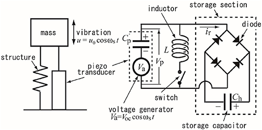
Figure 1. Outline of synchronized switch harvesting on inductor (SSHI) system.
Download figure:
Standard image High-resolution imagewhere  is the amplitude of the open-circuit voltage of the piezoelectric element and
  represents a piezoelectric constant.
Let  denote the charge in the piezoelectric element. The voltage across the piezoelectric element is given by

The characteristics of each diode of the bridge rectifier are modeled as follows:
where  is the applied voltage,
  is the forward current,
  is the FVD, and
  is the on-state resistance of the diode. In the SSHI method, the switch is turned on whenever
  reaches its maximum or minimum, and the on-state remains for half the period of the electrical vibration in the main circuit. If switching is repeated, the
  amplitude increases, and some energy is stored in capacitor
  when the absolute value of
  exceeds
  , where
  is the voltage of
  .
.
We assume that each component in the circuit, including the piezoelectric element, has an equivalent series resistance [21]. We denote the equivalent series resistances of the piezoelectric element, inductor, and on-state switch as  ,
,  , and
, and  , respectively. Figure 2 shows typical steady behaviors of
  and
and  . At
. At  , we assume that
  =
=  and
and


Figure 2. Typical behavior of  and
and  during SSHI.
Download figure:
Standard image High-resolution imageHence,  and
and  at this instant are given by


Let us further assume that  reaches maximum
  , and the switch is turned on at this moment. The subsequent behavior of
  is described as

Moreover, we assume that the system is designed such that  , and thus we can regard
  as constant during the subsequent period of
  , where

Considering the initial values, the solution of equation (7) can be obtained as follows:

Then, the values of  ,
,  , and
, and  at
at  are derived as


and  , where
  is an inversion factor. Therefore, as shown in figure 2, the value of
  jumps from
  to
to  , and its polarity inverts almost immediately.
In the subsequent half period of structural vibration,  , the switch is kept open, and thus
  remains constant, whereas
  varies toward
  as
as  varies from
  to −
to − . Once
  attains the value of
  , electric current
  flows through the bridge rectifier and storage capacitor, as shown in figure 2, and
  is charged. Voltage
  can be considered constant because capacitance
  is large and the effect of
  is negligible. Hence,
  remains at
  , as shown in figure 2. Moreover, the electric charge of
  is added to
  by
by  . Equation (4) holds at this instant, and the switch is turned on again. The subsequent behavior is the same as that described above except for the inverted polarity of some variables.
From the steady-state assumption and considering the behavior in figure 2, we can note that  . After some manipulations of equations based on this relation, we observe that the following energy term:

is additionally stored in  per structural vibration cycle. Equation (13) shows that no energy is additionally stored when
  increases to
  unless the stored energy is consumed or transferred to another storage component.
3. S3HI
3.1. Overview
When the current in an inductor varies quickly, the inductor generates a high voltage called a surge voltage. In SSHI, the switch is turned off when the current in the inductor is zero. Therefore, a surge voltage is not generated. Even when a surge voltage appears, the circuit in figure 1 cannot use it to increase the stored energy in  . Therefore, to exploit the surge voltage, the SSHI system should be modified in two aspects.
First, the circuit is modified such that the surge voltage enhances energy storage. Figure 3 depicts two such circuits. No components have been added to the original SSHI circuit. A rectifier can be connected to the main circuit in three ways: (a) across the piezo element (circuit P in figure 1), (b) across the inductor (circuit I in figure 3(a)), or (c) across the switch (circuit S in figure 3(b)). The SSHI approach uses circuit P, whereas the conventional and high-frequency S3HI approaches [19, 20] use circuit I. The last circuit, S, has not been investigated using the S3HI approach. In addition, when the switch in circuit S remains open, the circuit appears similar to that used in the standard FBR method. Therefore, given a large vibration amplitude, circuit S might harvest some energy without the need for switching control, thereby resulting in an auto-reboot of a system undergoing shutdown owing to complete battery discharge. Therefore, it is important to investigate how circuit S performs in accordance with the S3HI strategy, albeit the realization of the auto-reboot feature is a topic for future research. Because the only difference between the three circuits is the rectifier connection, their behaviors can be described by a single equation if no current flows through the rectifier.
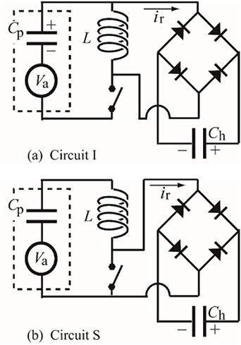
Figure 3. Circuit topologies to exploit surge voltage—(a) circuit I (bridge rectifier connected across inductor) and (b) circuit S (bridge rectifier connected across switch).
Download figure:
Standard image High-resolution imageSecond, the switching pattern for voltage inversion is modified to generate surge voltage. Figure 4 shows four switching patterns. Pattern S keeps the switch turned on for period  synchronized with half the period of the electric vibration, as described in section 2, and thus it does not generate surge voltage. Pattern E keeps the switch turned on for period
  , which is shorter than
  . This pattern generates a surge voltage at the end of the voltage inversion. Pattern H turns the switch on and off at a high frequency during the period
  . We propose pattern B, which maintains the switch in the ON state for period
  , turns it OFF for a short period
  , and finally maintains it in the ON state for period
  . This switching pattern generates a surge voltage close to the beginning of the voltage inversion. Voltage inversion decreases the energy stored in the piezoelectric element to
  times (i.e. less than 2/3 even when
  is as large as 0.8). Pattern B aims to transfer the energy before it dissipates.

Figure 4. Switching patterns for conventional SSHI and surge-induced synchronized switch harvesting on inductor (S3HI).
Download figure:
Standard image High-resolution imageWe analyzed the combinations of both circuits (I and S) in figure 3 with every switching pattern, E, H, and B, in figure 4. Note that the conventional SSHI combines circuit P and switching pattern S. The combinations of circuit I with switching pattern E (S3HI) [19] and circuit I with pattern H (high-frequency S3HI) [20] have already been studied. Note that we refer to all the combinations exploiting surge voltage as S3HI and indicate the circuit and switching pattern to identify the combination (e.g. IE indicates S3HI combining circuit I with switching pattern E). The circuit S and switching pattern B constitute our proposed configuration in this study.
In the remainder of this section, we analyze the typical operation of the different methods in the S3HI family. Approximate performance estimates are also derived, except for the cumbersome combinations IH and SH. Figure 5 shows the typical behaviors of voltage  and currents
  and
and  in long and short time scales.
  in figure 5(a) denotes the value of
  upon completion of voltage inversion, and its value according to the combination is indicated in the figure legend

Figure 5. Typical behaviors of  ,
,  , and
, and  according to S3HI combination—(a) general behavior over a long period along with specific behaviors over a short period for combinations of (b) IE, (c) IB, (d) IH, (e) SE, (f) SB, and (g) SH.
Download figure:
Standard image High-resolution image3.2. IE
IE uses circuit I and switching pattern E. Similar to SSHI, IE turns the switch on when  reaches its maximum or minimum and turns it off after period
  . In IE,
  for
for  to generate surge voltage.
We use the assumptions from section 2 unless otherwise stated. If no current flows through the bridge rectifier of circuit I, the electric behavior of circuit I is described by equation (7). Therefore, as described in section 2, the values of  ,
,  , and
, and  at
at  can be derived from equation (7) as follows:


where  . The switch is turned off at
  . Then, it is clear from figure 3(a) that subsequently
  and
and  hold. However, the current in the inductor cannot vary instantly. Therefore, current
  starts to flow through the inductor, rectifier, and
  , charging
  as shown in figure 5(b). Thus, the induced surge voltage overcomes voltage barrier
  .
.
The subsequent behavior of  is described as

where  ,
,  , and
, and  is the total series resistance of two diodes and the storage capacitor. We assume that
  is sufficiently large, and
  can be considered constant. After some manipulations of equation (17), we observe that
  ceases to flow at
  , and the increment of charge in
  by this moment is given by

where  . In the next half period of structural vibration (
 ) the switch is kept open, and thus
  remains constant. In contrast,
  varies from
  to
to  as
as  varies from
 to −
to − . As the system operates in steady state,
  , as shown in figure 5(a). Therefore, from equation (16), we obtain

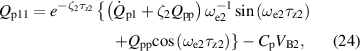
In the next half period of structural vibration,  is additionally charged by the amount described in equation (18). Therefore, the energy stored in
  per cycle of structural vibration is given by
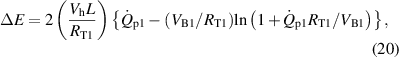
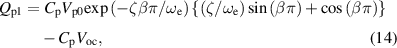
where  is obtained by substituting equations (15) and (19) into equation (20). Note that the above analysis is limited to the typical case in which
  given by equation (19) satisfies equation (4).
3.3. IB
IB uses circuit I and switching pattern B for the energy in the piezoelectric element to be harvested at the beginning of voltage inversion. We use the assumptions from section 3.2 unless otherwise stated. If the switch is turned on at  and turned off at
  , the charge given by equation (18) is additionally stored in storage capacitor
  during subsequent period
  , and the values of
  ,
,  , and
, and  at
at  are respectively given by equation (14),
  , and equation (16) assuming that
  . For IB, we assume that
  , which typically results in
  , as shown in figure 5(c). IB then turns the switch on again at
  to complete voltage inversion. Then, as described in section 2, voltage inversion is completed at
  .
.
IB typically turns the switch off at this moment. As in section 2,  at this moment can be derived from equation (11) as follows:

As in section 3.2, it is clear that  , and thus
  is given by

The amount of energy stored per cycle of structural vibration is given by equation (20) and can be obtained from equations (15) and (22).
3.4. SE
SE uses circuit S and switching pattern E. We use the assumptions from section 3.2 unless otherwise stated. If no current flows through the bridge rectifier, the behavior of circuit S can be described by equation (7). Therefore, the values of  ,
,  , and
, and  at
at  (i.e.
(i.e.  ,
,  , and
, and  ) are respectively given by equations (14)–(16). SE turns the switch off at this moment. As current
  cannot vary instantly, it starts to flow through the piezoelectric element, inductor, diode, storage capacitor, and next diode, charging the storage capacitor as shown in figure 5(e). Hence,
  , and the subsequent behavior of
  is described as

where  and
and  . After some manipulations of equation (23), we can see that
  at
at  , as shown in figure 5(e), completing voltage inversion. In addition,
  at this moment is given by
with

where  ,
,  , and
, and  . Moreover,
  at this moment is given by

The additionally stored charge in the storage capacitor within this period  is equal to the corresponding decrease in
  :
:

As shown in figure 5(a), after voltage inversion,  varies from
  to
to  as
as  varies from
  to
to  . If
. If  , current
  starts to flow when
  reaches
  while varying toward
  . However, we omit this case because it is rare, as analyzed below. Hence, we assume that
  and focus on the typical case. As the system is in steady state,

Unlike IE and IB, we need to solve algebraic equation (28) and the above equations to obtain the value of  for SE. Once we determine
  ,
,  can be obtained by substituting equations (14) and (24) into equation (27). In the next half period of structural vibration,
  is additionally charged by the amount described in equation (27), and the energy stored per period of structural vibration is given by

3.5. SB
SB drives the switch in the proposed circuit S according to the proposed switching pattern B shown in figure 4. We use the assumptions from section 3.4 unless otherwise stated. Again, if the switch is turned on at  and turned off at
  , the charge given by equation (27) is additionally stored in capacitor
  during the next period
  , and
, and  ,
,  , and
, and  at
at  are respectively given by equation (24),
  , and equation (26), provided that
  .
.
For SB, we assume that  , and therefore
  is positive as shown in figure 5(f). SB turns the switch on again at this moment and turns it off at
  . Subsequently,
  becomes zero, and this completes the voltage inversion, as shown in figure 5(f). The value of
  at this moment is given based on equation (11) by

We assume that  to focus on the typical case. Then, as described in section 3.4, it is clear that

in the steady state. Therefore,  can be obtained by solving equation (31). The amount of energy stored per period of structural vibration is obtained from equation (29) along with equations (14), (24), and (27), and
  can be obtained accordingly.
3.6. IH and SH
IH turns the switch of circuit I on at  , off at
  , on at
  , off at
  , and so on. Typically, voltage inversion is expected to complete when the switch is turned off at
  , where
  is the number of periods
  .
.
SH controls the switch of circuit S like IH. The typical behaviors of  ,
,  , and
, and  are illustrated in figures 5(d) and (g) for IH and SH, respectively. The energy stored per cycle of structural vibration can be derived by using the equations derived in the previous sections. However, they are not shown here for brevity.
4. Numerical simulations
In section 3, algebraic equations to estimate the performance of each method are derived for typical cases. To investigate and evaluate thoroughly the methods in the S3HI family including the omitted cases, we conducted numerical simulations. We derived the governing equations from Kirchhoff's law and performed numerical integration using the Runge–Kutta method.
4.1. Governing equations
As the considered system includes diodes, it is convenient to describe the governing equations for the six states listed in table 1. Let  denote the current flowing through the bridge rectifier as shown in figures 1 and 3. To write the equations compactly, we introduce variable S, whose value is shown in table 1 according to the switch state and polarity of
  . Table 1 lists the applicable governing equations per state:


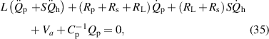


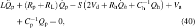


Table 1. Switch states, values of S, and applicable governing equations per case considered in numerical simulations.
| Governing equations | |||||
|---|---|---|---|---|---|
| Switch state | Polarity of 
| S | Circuit P | Circuit I | Circuit S |
| Off |

| S = 1 | (32), (33) | (36), (37) | (32), (40) |

| S = −1 | ||||

| S = 0 | (32), (34) | (34), (36) | (32), (34) | |
| On |

| S = 1 | (33), (35) | (38), (39) | (41), (42) |

| S = −1 | ||||

| S = 0 | (34), (35) | (34), (39) | (34), (42) | |
4.2. Simulation program
The simulation program was scripted in Fortran wherein the applicable governing equations were selected in accordance with table 1 based on the switch and current  states. The equations were numerically integrated to evaluate
  , and
, and  . The states of the switch and
  were checked at each successive time instant, and if any state demonstrated a change, the corresponding governing equation to be integrated was changed to its applicable form. When the governing equations were changed, the current flowing through the inductor and the charge of the capacitors were maintained at a constant value. Updated values of other variables were calculated using the governing equations prior to proceeding to the next time step. All simulations were performed under double precision on a PC (Panasonic CF-LX3; Osaka, Japan). The magnitude of the time-step increment equaled 7.64 ×10⁻⁹ s.
4.3. Results from simulations and approximate equations
To evaluate the approximate equations and numerical simulations, we obtained the corresponding energy harvesting performances of SSHI, IE, SE, IB, and SB using the same input data. The circuit parameters are listed in table 2. The parameter values were determined by measuring those of actual components from the corresponding experimental setup. In addition, the switching timing listed in table 3 was used to obtain the performances. The timing values were obtained from the values in table 4, which lists near-optimal experimental values. Because we assumed that  when an approximate result is obtained, the value of
  was set to 10 000 during simulations performed in this study. We also analyzed excitation frequencies of 100 and 25 Hz.
Table 2. Parameters of energy harvesting circuit.
| Parameter | Value | Unit |
|---|---|---|

| 1.41 | μF |

| 4.7 | μF |
| L | 10.5 | mH |

| 4.5 | Ω |

| 0.5 | Ω |

| 5.5 | Ω |

| 10 | Ω |

| 0.65 | V |

| 100 | nF |

| 200 | nF |

| 420 | Ω |

| 340 | Ω |
Table 3. Switching timing to obtain simulation and approximate results.
| Method | SSHI | IE and SE | IB and SB | ||
|---|---|---|---|---|---|
| Parameter |

|

|

|

|

|
| Value | 1 | 0.781 | 0.206 | 0.126 | 1.310 |
Table 4. Near-optimal switching times obtained from experiments at  .
.
| Method |

|

|

|

| Additional parameters |
|---|---|---|---|---|---|
| IE | — | — | 0.781 | 5.12 | — |
| SE | — | — | 0.794 | 5.23 | — |
| IH | 0.264 | 0.0096 | 1.045 | 5.45 |
 = 3.82, duty = 0.964 = 3.82, duty = 0.964 |
| SH | 0.264 | 0.0096 | 1.045 | 5.58 |
 = 3.82, duty = 0.964 = 3.82, duty = 0.964 |
| IB | 0.206 | 0.126 | 1.310 | 6.60 |
 = 0.979, duty = 0.904 = 0.979, duty = 0.904 |
| SB | 0.182 | 0.107 | 1.241 | 6.62 |
 = 0.955, duty = 0.916 = 0.955, duty = 0.916 |
Note: Duty is defined in the footnote of table 5.
Table 5. Optimal switching timing at  , corresponding
  , and effect of precise optimization.
| Method |

|

| Duty |

| Increment |
|---|---|---|---|---|---|
| IE | — | 0.807 | — | 5.20 | 0.08 |
| SE | — | 0.779 | — | 5.27 | 0.04 |
| IB | — | 1.245 | 0.952 | 6.73 | 0.13 |
| SB | — | 1.229 | 0.939 | 6.90 | 0.28 |
| IH | 2 | 1.020 | 0.970 | 5.76 | 0.31 |
| 3 | 1.020 | 0.970 | 5.79 | 0.34 | |
| 4 | 1.010 | 0.970 | 5.80 | 0.35 | |
| SH | 2 | 0.985 | 0.968 | 5.87 | 0.29 |
| 3 | 0.985 | 0.970 | 5.89 | 0.31 | |
| 4 | 0.980 | 0.970 | 5.90 | 0.32 |
Note: For IB and SB,  ; for IH and SH,
  . The increment in
  (last column) is due to precise optimization
Figure 6 depicts the results obtained from numerical simulations and approximations. For the sake of clarity, the results obtained for IE and SB are not shown. The values of the normalized energy harvested per structural-vibration cycle (i.e.  ) are plotted against those of Vh/Voc. As can be observed, the assumptions considered to derive the approximate equation are satisfied in all cases. When considering IE and SB as well, the maximum difference between the values of
  obtained using the approximate equation and numerical simulation equals 0.67 at a 100 Hz excitation frequency, whereas it remains below 0.1 at a 25 Hz excitation frequency. This is consistent with the assumption
  considered to derive the approximate equation. Therefore, the approximate equations demonstrate good agreement with the numerical-simulation results.
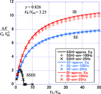
Figure 6. Harvesting performances obtained from approximate equations and numerical simulations.
Download figure:
Standard image High-resolution image4.4. Numerical-simulation results
To verify the experimental results reported in section 5, we obtained the corresponding results from numerical simulations. The circuit parameters listed in table 2 were used, except for  and
and  for SSHI, which were set as described in section 5.2. In addition, the experimental switching timing listed in table 4 was used, and
  was set to 10 000. First,
  was charged up to voltage
  to set an initial condition, and integration continued over 50 cycles of mechanical vibration. After confirming that the system reached the steady state, the stored charge per cycle was obtained by integrating
  .
.
5. Experiments
To determine if each method in the S3HI family operates as expected, we conducted verification experiments.
5.1. Experimental setup
Figure 7 depicts the mechanical setup for vibration-energy harvesting. As can be seen in figure 7(a), a conical metal fitting adheres to each end of a stack piezoelectric element (PICMA P-885.51; PI Ceramic, Lederhose, Germany). Additionally, the semiconductor strain gauges (KSP-1-350-E4; Kyowa, Tokyo, Japan) adhere to the side surfaces of the element, thereby evaluating the axial strain therein. Subsequently, the element was clamped between the dints on the support structure and cantilevered plate. Thus, the element was compressively preloaded, as depicted in figures 7(b) and (c). The support structure comprised a rod with adjustable length. An 8 kg mass was mounted on the plate, which was sinusoidally excited at 100 Hz frequency by an electromagnetic shaker (WF1974; Akashi Seisakusho, Tokyo, Japan), whereas the resonant frequency was 144 Hz.
Figure 7. Experimental setup.
Download figure:
Standard image High-resolution imageFigure 8 shows a diagram of the electrical setup for the experiments. Channel 1 of the function generator (WF1974; NF corporation, Kanagawa, Japan) provided a 100 Hz sinusoidal signal, which was amplified and fed to the shaker to induce mechanical vibration. The switch shown in figures 1 and 3 was implemented using two field effect transistors (FETs; 2SK4017; Toshiba, Tokyo, Japan). Channel 2 of the function generator provided a 200 Hz square wave, whose amplitude, duty, and phase delay with respect to channel 1 were controllable. To drive the FET switch, the output from channel 2 was directly used when applying switching pattern S or E (figure 4). For switching pattern B, the output from channel 2 was modified using RC delay circuits and logic components and fed to the switch. For switching pattern H, the output from channel 2 was modified by using the output from a clock generator (TL494IN; Texas Instruments, Dallas, TX, USA), which provided a square signal. The frequency and duty of the output were adjustable by modifying the resistance and capacitance of the clock generator (not shown in figure 8). Therefore, all the circuits, P, I and S (figures 1 and 3), and all the switching patterns, S, E, H, and B (figure 4), could be implemented by adjusting the function generator, variable resistances of the RC delay circuits, capacitor, and variable resistance connected to the clock generator, and three snap switches shown in figure 8. The inductor in the circuit was a model ELC18B103L (Panasonic, Osaka, Japan), and the diodes composing the rectifier were of model 1N4148TR (Vishay Intertechnology, Malvern, PA, USA). The various voltages were measured typically via unit-gain buffers using an Analog–Digital converter board (LPC-320724; Interface, Hiroshima, Japan) connected to a desktop PC. The unit-gain buffers used OPA445AP (Texas Instruments, Dallas, TX, USA) as the operational amplifier. A signal conditioner (CDV-230 C, Kyowa, Tokyo, Japan) was used for strain measurements. Figure 9 shows a picture of the circuit, where the jumper lines for voltage measurement at various points were removed. The phase difference between the outputs from channel 2 of the function generator and clock generator was not controllable.

Figure 8. Electrical setup for experiments.
Download figure:
Standard image High-resolution image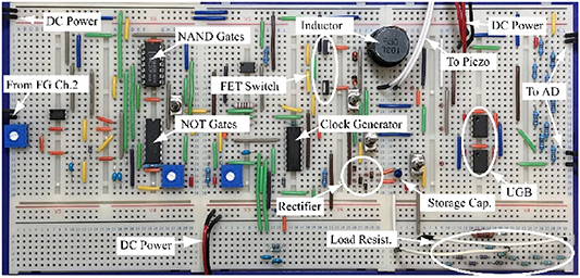
Figure 9. Circuit used during experiments performed in this study. Note: FG: function generator, AD: A-D converter, UGB: unity gain buffer.
Download figure:
Standard image High-resolution image5.2. Experimental parameters
The parameters of the components for the experiments were measured using an LCR meter at a frequency of 1.3 kHz, which is close to  . The relation between the applied voltage and current of the diode was measured as shown in figure 10. In this experiment of S3HI, the current through the diodes was approximated to 5 mA from preliminary experiments and simulations. Therefore, the values of
  and
and  were estimated from the tangent around 5 mA, as shown in figure 10. The identified parameters are listed in table 2, which provides the important parameters of this system, including
  ,
,  , and
, and  at
at  . On the other hand, the current through the diodes was estimated to be below 10
  when applying SSHI. Therefore,
  and
and  for SSHI were 0.45 V and
  , respectively, as obtained from figure 10. These values were used only when we compared the experimental and simulation results.
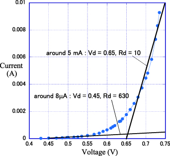
Figure 10. Voltage–current relation for diode 1N4148TR.
Download figure:
Standard image High-resolution image5.3. Experimental procedure
Because S3HI facilitates energy harvesting from low-amplitude vibrations, the output amplitude from channel 1 was adjusted such that the amplitude of open-circuit voltage of the piezoelectric element  equaled 0.2 V. This value of
  is equivalent to a strain of 1.74 μ for an 18 mm long piezoelectric element. The value of
  was manually adjusted by monitoring the temporal evolution of
  and/or strain values obtained from the strain gauges attached to the piezoelectric element. For each method in the S3HI family, load resistor
  , which makes the value of
  to be approximately 2 V, was first connected to the storage capacitor as shown in figure 8. Then, the switching timing was manually adjusted to maximize
  . The obtained and measured switching timings are listed in table 4. Typical values of
  and
and  in figure 8 obtained via tuning are listed in table 2. As these values were manually obtained during experiments, they can be considered near-optimal.
Subsequently, by maintaining this condition for each method, the load resistance was varied with different resistors. By measuring  , the energy stored in a period of structural vibration was obtained as
  . To characterize the operation of each method, we measured various voltages, including
  , voltage across the inductor, and voltage across the switch, through unity-gain buffers.
5.4. Comparison between experimental and simulation results
Figure 11 shows the experimental and simulation results of energy harvested per vibration cycle obtained for each evaluated method. The normalized performance,  , is shown according to the normalized voltage of the storage capacitor,
  . The experimental results are mostly consistent with the simulation results. The performance depends on the switching pattern but is almost independent of the circuit topology (i.e. circuit I or S). These results may not correspond to the maximum performance of each method because the switching timing was roughly optimized to
  .
.
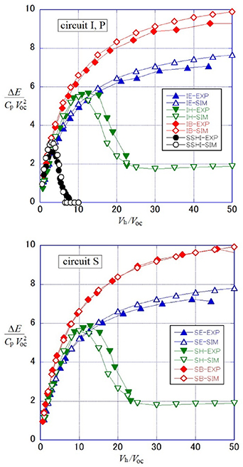
Figure 11. Experimental and simulation results of performance obtained from different methods.
Download figure:
Standard image High-resolution imageWhen IE or SE is applied, figure 11 shows that the experimental and simulation results suitably agree. Figure 12 shows a close-up view of the experimental and simulation evolution of the input voltage to the bridge rectifier of circuit I (i.e. voltage across the inductor) for IE. The curves virtually coincide. When the switch is turned off after keeping it on for period  , a high voltage is induced, and the storage capacitor is charged at the end of voltage inversion, overcoming the voltage barrier of
  .
.

Figure 12. Evolution of experimental and simulation results of input voltage to bridge rectifier for IE.
Download figure:
Standard image High-resolution imageThe experimental and simulation results differ by the high-frequency vibration in the experimental curve. This vibration may be generated by the stray capacitance and the inductor. The vibration frequency of 112 kHz and inductance of 10.5 mH result in a stray capacitance of 0.192 nF. The vibration amplitude suggests an energy dissipation of approximately 7.01 × 10⁻¹⁰ J, being around 0.15% of the mechanical vibration converted into electrical energy. Therefore, the dissipation is negligible. Figure 13 shows the evolution of  and
and  in a longer time scale. The value of
  jumps at every voltage inversion, showing that some energy is added as intended in the proposed design.
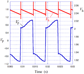
Figure 13. Experimental values of  and
and  over a long period for IE.
Download figure:
Standard image High-resolution imageFigure 11 reveals that the discrepancy between the experimental and simulation results of the performance estimation for IH and SH is relatively large when  , possibly due to the estimation error of
  . As
. As  is shorter than 4 μs, it is difficult to obtain an accurate measure from data sampled at 1.54 MHz. If we consider a shorter
  , the discrepancy decreases.
Figure 14 shows the evolution of the experimentally obtained input voltage to the bridge rectifier during voltage inversion for IH. The switch is turned off four times within period  , generating a high voltage and charging the storage capacitor four times during one voltage inversion process.
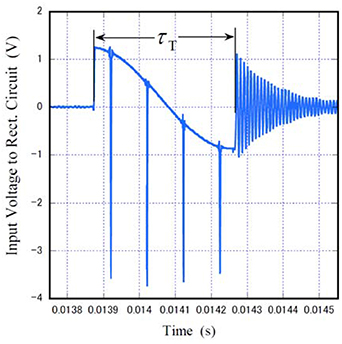
Figure 14. Evolution of input voltage to bridge rectifier for IH.
Download figure:
Standard image High-resolution imageFigure 11 shows that IB and SB outperform the other S3HI methods. Figure 15 shows the experimental and theoretical evolution of the input voltage in the bridge rectifier of circuit S (i.e. voltage across the switch) for SB. As is the case for IE, both curves coincide except for the high-frequency vibration that appears in the experimental results whenever the current ceases to flow. Such high-frequency vibration may also be related to the stray capacitance, and its effect on harvesting is negligible.
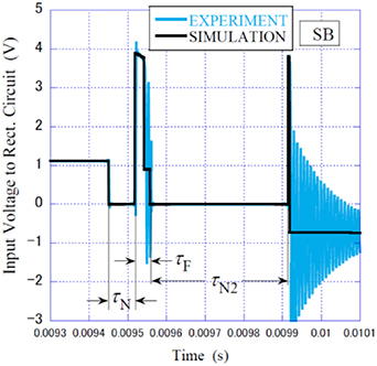
Figure 15. Evolution of input voltage to bridge rectifier for SB.
Download figure:
Standard image High-resolution imageFigure 16 shows the evolution of the experimentally obtained  and
and  in long and short time scales. Figures 15 and 16 show that a high surge voltage is induced, and the storage capacitor is charged near the beginning of voltage inversion, overcoming the barrier of
  as designed. The voltage pulse at the end of period
  indicates that
  is slightly shorter or longer than
  .
.

Figure 16. Evolution of  and
and  for SB.
Download figure:
Standard image High-resolution image6. Evaluation of S3HI methods
6.1. Effect of precise switching timing optimization
The preceding sections of this paper discussed the investigation and comparison of the performance of the different S3HI methods using near-optimal switching times obtained via experiments. This section discusses the corresponding investigations and comparisons performed after precise optimization of the switching time. We determined two sets of optimal switching timings through simulations to maximize  at
at  and
and  . We fixed
  to 0.2 V like in the experiments. For IB and SB, the optimal value of
  is approximately 0.99–0.98 in many cases. However, even when the other two parameters are optimized while maintaining
  at 1.0,
  decreases only by 0.1% compared with the optimal value. Therefore, we fixed
  to 1.0 and considered the other two parameters as design parameters. In IH and SH,
  was considered to be an integer, and the optimal values of the other two independent parameters were searched for
  2, 3, and 4. Table 5 lists the obtained optimal timings, maximum values of
  at
at  , and increments of
  due to the precise optimization.
By using the optimal switching timing, we performed various numerical simulations. Figure 17 shows the performances of the SSHI and S3HI methods at various values of  . For IH and SH,
  is almost independent of
  , as listed in table 5. Therefore, figure 17 only shows the case for
  . As shown in table 5 and by comparing figures 17 and 11, the performance improvement due to the precise optimization of the switching timing is negligible. Hence, the methods in the S3HI family are relatively robust to variations in switching timing, with IE and SE being the most robust, IB and SB being moderately robust, and IH and SH being the least robust methods.
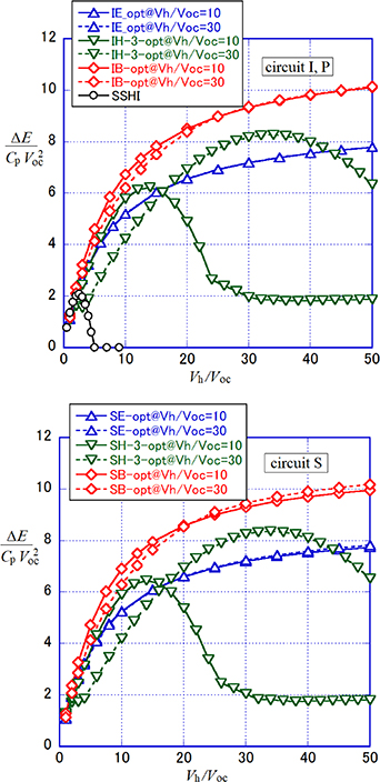
Figure 17. Performance of S3HI methods under small-amplitude vibrations and/or large FVD ( ) with switching times optimized for
  and
and  .
.
Download figure:
Standard image High-resolution image6.2. Comparison of the methods under low-amplitude vibration or large FVD
Figure 17 shows that SSHI can harvest energy in a limited range of  , whereas any method in the S3HI family achieves harvesting in a wider range beyond the values shown in the figure and can harvest more energy. Even for cases in which SSHI can harvest, its performance (i.e.
  ) is much lower than that of the methods in the S3HI family. In addition, the curve showing the relation between
  and
and  depends on the value of
  at which switching timing is optimized. This dependency is strong in IH and SH and weak in IE and SE. Regarding both peak performance and average performance, SB and IB provide the highest values. Hence, the proposed switching pattern B substantially enhances the performance of S3HI. Figure 17 reveals that when
  , the switching pattern B demonstrates a harvesting performance that has increased by 11%–31% and 15%–450% compared to patterns E and H, respectively, depending on the
  value.
As observed, SE, SH, and SB demonstrate slightly better performance compared to the IE, IH, and IB, respectively, at  values corresponding to optimum switching times, as indicated by the value of
  listed in table 5. However, the observed differences in table 5 and figure 17 are marginal. This demonstrates that circuit S is a good alternative to circuit I.
6.3. Performance of methods in S3HI family under large-amplitude vibrations or small FVD
We have exclusively focused on small-amplitude vibrations and large FVD (i.e.  ) in the simulations and experiments reported thus far in this paper, because this is the main operating condition considered in this study. However, we have also investigated the performance and characteristics of the different methods in the S3HI family under conditions of large-amplitude vibration and/or small FVD (i.e.
  ). More specifically, we set
  , and the other parameters were set as listed in tables 2 and 5. Hence, the switching timing was not optimized for
  .
.
Figure 18 shows the harvesting performance of SSHI, SE, SH, and SB for  . Similar to figure 17, figure 18 reveals that SSHI can harvest energy only when
  is lower than a certain value, whereas all the methods in the S3HI family achieve harvesting over a wide range of
  values beyond that shown in the figure. Therefore, S3HI can store significantly more energy than SSHI when
  . Unlike the case wherein
  , SSHI provides the highest performance when
  . Otherwise, SB provides the highest performance. If the switching timing is optimized for
  , the performance of each method in the S3HI family increases. However, the performance increase at
  and
and  due to this optimization is below 0.12 for SE and 0.75 for SB. In practice, this increase is considered negligible. Hence, the timing parameters determined at
  for SE and SB can be used in practice even when
  assumes a large value of 6.5 V. This demonstrates the robustness of the proposed strategy to variations in the vibration amplitude.
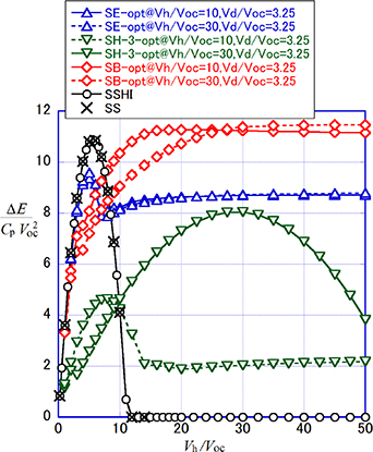
Figure 18. Performance of SSHI, SE, SH, SB, and SS under large-amplitude vibration and/or small FVD ( ).
).
Download figure:
Standard image High-resolution imageAs discussed above, we have demonstrated that the performance of the proposed circuit S is equivalent to that of circuit I. Nevertheless, the use of circuit S might provide additional advantages when vibration amplitude is large or  is small. Figure 18 demonstrates the performance of the SS method, which is an energy-harvesting method based on the combination of circuit S and switching-pattern S. Therefore, when circuit S is used, SS and SB become interchangeable via a simple change in the switching pattern from S to B and vice versa. Figure 18 reveals that the performances of SS and SSHI are identical and that they outperform other methods when
  When
When  7, SB outperforms other methods. This fact indicates that one can always attain the best performance by using circuit S and adaptively selecting the preferred switching pattern between B and S depending on the
  value.
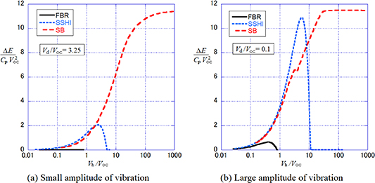
6.4. Comparison of performance of SB from S3HI family with that of passive FBR and certain other methods
Figure 19 compares the performances of passive FBR, SSHI, and SB (a typical member of the S3HI family). The FBR circuit was implemented by neglecting the switch and inductor of the circuit P shown in figure 1. Thus, the performance of FBR was obtained using the simulation program described in section 4.2, keeping the switch open. The parameter values listed in table 1, which were used in all the numerical simulations in this study, were used in this simulation as well. The value of  was 0.65 V. The switching timings for SB were
  and duty = 0.97, which are optimal at
  = 30 and
  = 3.25. The value of FVD was
  = 0.65 V, and the vibration frequency was 100 Hz. Figure 19(a) shows the case of small-amplitude vibration, which is the target condition of this study. The figure shows that the FBR harvests no energy in this case, irrespective of the storage-capacitor voltage. However, SB achieves a high harvesting rate even when
  is large and the vibration amplitude is small. This figure depicts well that SB performs effectively from the perspective of our objective. Figure 19(b) shows the case of large-amplitude vibration; in this case, FBR can harvest some energy only when
  is relatively small. SB realizes a high harvesting rate when
  is large, in this case as well.
Figure 19. Comparison of performance of a typical member of the S3HI method with that of passive FBR and SSHI.
Download figure:
Standard image High-resolution image
Table 6 summarizes figure 19. Power enhancement is defined as  in this study; max and
  are defined in the footnote of table 6. When the amplitude of open-circuit voltage
  is as small as
  , power enhancement is infinity because
  .
.  denotes the maximum value of
  at which
  holds, and
  denotes the upper limit of storable energy. Because no energy is additionally harvested when
  , the upper limit is given by
  .
.
Table 6. Comparison of performances of SBR, SSHI, and S3HI-SB.
| Publication |

|

| Method |

| Power enhancement |

|

|
|---|---|---|---|---|---|---|---|
| This work | 3.25 | 0.826 | S3HI-SB | 11.4 |

| >1000 | >5.0 × 10⁵ |
| SSHI | 2.08 |

| 4.8 | 11.5 | |||
| FBR | 0 |

| 0 |

| |||
| 0.1 | 0.826 | S3HI-SB | 11.5 | 18.0 | >1000 | >5.0 × 10⁵ | |
| SSHI | 10.9 | 17.1 | 11.5 | 66.1 | |||
| FBR | 0.639 | 1 | 0.80 |

| |||
| [3] | 0 | — | SECE | 4.0 | 4.0 |

|

|
| [6] | 0 | 0.822 | Series SSHI | 10 | 10 | 1.0 | 0.50 |
| [7] | 0 | 0.74 | Hybrid SSHI 1) | 7.7 | 7.7 | 30 | 450 |
| [10] | 0 | 0.8 | ESSE 2) | 8.0 | 8.0 |

|

|
| [14] | 0 | 0.7 | SICE 3) | 6.4 | 6.4 |

|

|
Note: Power enhancement:  , max: maximum value with respect to Vh/
 ,
,  : energy harvested per vibration cycle,
  : value of
  of FBR. 1) Transformer ratio
  , 2) efficiency of buck-boost converter
  = 0.9, 3) energy transfer efficiency
  .
.
Table 6 shows the performance of certain previously proposed methods as well. When the value of  was not included in a study, it was calculated from the corresponding values of load resistance and harvested power in each study. Unfortunately, values of parameters such as
  and γ are different in each case. However, table 6 shows that
  is very large when S3HI-SB, SECE, ESSE, or SICE is applied. In principle,
  decreases when
  increases. However, table 6 shows that when S3HI-SB is applied, value of
  is larger than those of prior methods even though
  in them. The objective of this study was not only to obtain a large value for
  , but also to increase the upper limit of the stored energy. Therefore, table 6 demonstrates that our objective is achieved well by, e.g. SB of the S3HI family.
7. Conclusions
In this paper, various vibration-energy harvesting methods based on piezoelectric transducers, establishing the S3HI family, were characterized and analyzed. These methods exploit the surge voltage generated by turning off the switch for short periods during the voltage inversion of the conventional SSHI. The underlying circuits for the methods in the S3HI family are as simple as the circuit for the SSHI method. By incorporating a novel circuit S and switching pattern B, we derived six methods in the S3HI family.
Simulation and experimental results as well as theoretical derivations demonstrate that the methods in the S3HI family generate surge voltage as designed and achieve efficient vibration-energy harvesting even when the open-circuit voltage of the piezoelectric element is much smaller than the FVD of the diodes in the bridge rectifier. This feature contrasts with the SSHI operation.
Of the six methods from the S3HI family evaluated in this study, SB and IB demonstrate equivalent performance. Therefore, the proposed switching pattern B outperforms the existing patterns E and H when implemented in either the proposed or conventional energy-harvesting circuits. In the case of low-amplitude vibrations, the proposed pattern increases harvesting performance by 11%–31% and 15%–450% compared to the existing patterns E and H depending on the  value. The proposed circuit S harvests the same energy per vibration period as a traditional circuit. However, it affords a potential auto-reboot capability. In addition, using circuit S, one can realize the best energy-harvesting performance by selecting an appropriate switching pattern. Therefore, the proposed circuit is a promising alternative to the S3HI configuration, although the realization of these concepts is a topic for future research. Lastly, this paper presented the characteristics of each method in the S3HI family. These included robustness against switching-time errors as well as that against variations in the vibration amplitude and storage-capacitor voltage.
Acknowledgments
This work was supported by JSPS KAKENHI Grant Number JP20K04373
Data availability statement
All data that support the findings of this study are included within the article.
Conflicts of interest
The authors have no conflicts of interest to declare.