
Abstract
This study addresses the complementary metal-oxide-semiconductor-compatible fabrication of vertically stacked Si/SiO2/Si nanopillars (NPs) with embedded Si nanodots (NDs) as key functional elements of a quantum-dot-based, gate-all-around single-electron transistor (SET) operating at room temperature. The main geometrical parameters of the NPs and NDs were deduced from SET device simulations using the nextnano++ program package. The basic concept for single silicon ND formation within a confined oxide volume was deduced from Monte-Carlo simulations of ion-beam mixing and SiOx phase separation. A process flow was developed and experimentally implemented by combining bottom-up (Si ND self-assembly) and top-down (ion-beam mixing, electron-beam lithography, reactive ion etching) technologies, fully satisfying process requirements of future 3D device architectures. The theoretically predicted self-assembly of a single Si ND via phase separation within a confined SiOx disc of <500 nm3 volume was experimentally validated. This work describes in detail the optimization of conditions required for NP/ND formation, such as the oxide thickness, energy and fluence of ion-beam mixing, thermal budget for phase separation and parameters of reactive ion beam etching. Low-temperature plasma oxidation was used to further reduce NP diameter and for gate oxide fabrication whilst preserving the pre-existing NDs. The influence of critical dimension variability on the SET functionality and options to reduce such deviations are discussed. We finally demonstrate the reliable formation of Si quantum dots with diameters of less than 3 nm in the oxide layer of a stacked Si/SiO2/Si NP of 10 nm diameter, with tunnelling distances of about 1 nm between the Si ND and the neighboured Si regions forming drain and source of the SET.
Export citation and abstract BibTeX RIS

Original content from this work may be used under the terms of the Creative Commons Attribution 4.0 license. Any further distribution of this work must maintain attribution to the author(s) and the title of the work, journal citation and DOI.
1. Introduction
Driven by the tremendous broadening of mobile and 'Internet-of-Things' applications, the development of low-power logic and memory circuits remains a main task for the next generation of energy-efficient electronic devices [1, 2]. Structures based on spintronics [3], two-dimensional (2D) materials [4] and tunnelling field-effect transistors made of compound semiconductors [5, 6] are among the favoured approaches for future low-power circuits. With respect to classical Si-based complementary metal-oxide-semiconductor (CMOS) transistor technology, down-scaling of device dimensions is the key for further power reduction [7, 8]. Presently, lateral fin field-effect-transistors (FinFETs) in the sub-8 nm node represent state-of-the-art technology, whereas stacked FinFET, ribbon or vertical nanowire (NW) transistor architectures enable real 3D-integration in the foreseeable future [9]. In 2013, Larrieu and Han [10] presented a silicon vertical NW transistor with gate-all-around (GAA) configuration fabricated in standard CMOS technology. These transistors with NW diameters of 20–80 nm offer excellent parameters with an 'on/off' ratio > 105 and a drain-source current of 10–100 nA [11, 12].
Another device type with extremely low energy dissipation is the dot-based single-electron transistor (SET) [13]. In this device, electrons tunnel from the drain to the source region via a quantum dot (QD). The blocking/non-blocking states of SET are controlled by the potential of the QD which can be tuned by a third electrode (gate) capacitively coupled to this dot [14]. Typically, SETs work only at cryogenic temperatures (<100 K) [15–17]. However, for many SET applications room-temperature (RT) operation is mandatory which requires a QD size of only a few nanometres to fulfil the Coulomb blockade condition [14]. SET structures operating at RT has already been realized, mainly based on lateral Si NWs [18–20], nanocrystalline Si [21] or metallic nanodots [22]. Numerous SET applications were proposed making use of its high charge sensitivity and low power consumption, see review papers [23, 24] and references therein. Examples are electrometers, DC current or temperature standards, microwave or infrared sensors, non-volatile memories or programmable logic circuits.
SETs are often considered as 'beyond-CMOS' devices, particularly when metallic or III–V semiconductor QDs are used. The novel SET device architecture considered in this work promises RT operation, CMOS-compatible fabrication and high-density integration. This concept is based on a Si nanodot (ND) embedded in the oxide of a vertically stacked Si/SiO2/Si nanopillar (NP). The capability for CMOS-compatible, monolithic integration of FETs and SETs is essential because SETs have intrinsic drawbacks, such as low gain, high output impedance or the disability to drive loads [24, 25]. Fortunately, SET and FET performances are complementary. Whereas SETs exhibit ultra-low power consumption, FETs offer advantages such as high speed, driving force, voltage gain and variable input impedance that compensate exactly for the SET limitations. As an example for an integrated SET/FET programmable logic device, logic functionality can be completely realized by the SET network by using QD based non-volatile memory structures, and only a limited number of FETs are required to drive the power-demanding components of the integrated circuit [26].
It has been proposed by Mahapatra and Ionescu [27] that hybrid SET/FET circuits with the FET operating at sub-threshold regime provide a way to preserve low power consumption. By on-chip SET/FET integration one can boost the Coulomb Blockade oscillation phenomenon of SET and the high drive current of FET. Thus, high performance and low energy dissipation are expected for such integrated SET/FET-CMOS architectures. They are able to address functionalities such as neuromorphic or multiple valued logic circuits which are very difficult to implement by classical FET-CMOS circuits alone [27]. Another application field is sensing, either as a single charge sensor for semiconductor-based quantum computing or as a biosensor system [28].
In this study, we describe a CMOS-compatible fabrication process to realize stacked sub-15 nm Si/SiO2/Si NPs with embedded silicon (Si) NDs as key building blocks for SET fabrication. The envisaged SETs have a vertical transistor topology with GAA electrode, similar to vertical NW FETs, what entails for high-density and monolithic FET/SET integration capability. The process flow combines top-down technologies, such as NP fabrication by electron-beam lithography (EBL) and reactive ion etching (RIE), with the bottom-up approach of Si ND self-assembly. Single (or a few) ND(s) in an oxide with small tunnelling distances to adjacent source/drain electrodes form by phase separation of a strongly confined, metastable Si-rich oxide (SiOx → SiO2 + Si) and Ostwald ripening during subsequent annealing. The SiOx (x < 2) is produced by ion-beam mixing of Si into the oxide from the two Si/SiO2 interfaces, whereas the spatial confinement required for single Si ND formation is defined by the small oxide volume within the NP.
The paper is organized as follows: at first, physical process and device simulations are presented in order to derive the required dimensions for the NP/ND as well as the basic parameters for ion-beam mixing. Then, the technology for NP/ND fabrication is described in detail, and the realized structures with nanometre dimensions are characterized using state-of-the-art electron and ion microscopy. It is shown that the applied technology is able to realize stacked Si/SiO2/Si NPs at diameters close to 10 nm with embedded single Si NDs of ⩽3 nm size, what will be suitable for SET operation at RT. For structures of only a few nanometres, variability of critical dimensions (CDs) represents a relevant device reliability aspect [29]. Thus, the impact of tunnelling distance differences or the variation of ND size and its position in the oxide disc on the performance of SETs is discussed in a separate section.
The integration of the NP/ND structures into the complex technology of SET/FET circuit fabrication is published in a separate paper [30]. The technologies introduced in both publications offer a unique path for the manufacturability of RT operating SETs and integrated SET/FET circuits.
2. Basic considerations and device simulations
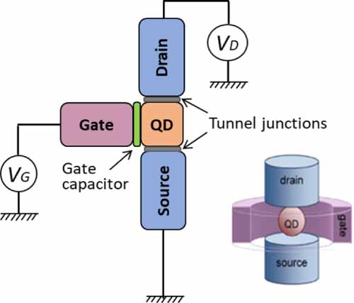
Figure 1 shows the basic scheme of a GAA NP SET. The QD, realized by the silicon ND, is separated by two symmetric tunnel junctions from the adjacent drain/source regions. The tunnelling current ID is a function of the drain-source voltage VD and the widths of the tunnelling barriers, while the 'on/off' state of the transistor is controlled by the potential VG of the outer circular gate electrode surrounding the ND region at the NP rim. The silicon ND size and tunnelling distances must be sufficiently small to drive a controllable and stable electron current at low voltages VD and VG.
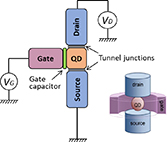
Figure 1. Schema of QD-based SET. The lower right inset illustrates a vertical, GAA SET configuration where the single Si QD is located in the centre of a SiO2 disc sandwiched between drain/source regions in the pillar. VG, VD denotes the gate-source and drain-source voltages, respectively.
Download figure:
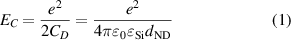
Standard image High-resolution imageTo enable RT operation of the SET, the Coulomb blockade [14] condition must be fulfilled, which means that the silicon ND electrostatic energy EC considerably exceeds the thermal energy kT to suppress the influence of thermal fluctuations. The electrostatic energy of the dot is calculated as
where CD
and dND denote the self-capacitance and diameter of the spherical Si ND, respectively;  0 is the permittivity, Si = 11.8 (Si dielectric number); e, k are the elementary charge and Boltzmann constant, respectively. According to equation (1), a ND diameter of dND ⩽ 3.5 nm is required to realize a barrier exceeding the common precondition Ec
> 10 kT ≈ 0.3 eV for RT operation of a quantum device.
0 is the permittivity, Si = 11.8 (Si dielectric number); e, k are the elementary charge and Boltzmann constant, respectively. According to equation (1), a ND diameter of dND ⩽ 3.5 nm is required to realize a barrier exceeding the common precondition Ec
> 10 kT ≈ 0.3 eV for RT operation of a quantum device.
Based on the nextnano++ program package [31], a simulation framework was developed to calculate the current–voltage (I–V) characteristics of such a stacked NP SET (as shown in figure 2) and to derive the main geometrical constraints as targeted values for NP/ND fabrication [32].
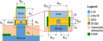
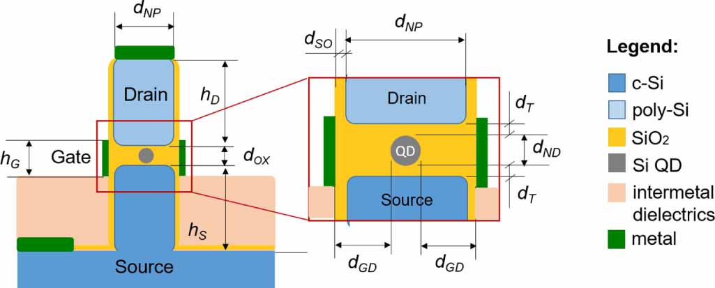
Figure 2. NP/ND as key functional components of the SET with their main geometrical parameters. Legend: hD,S,G: height of drain, source or gate; dOX: oxide thickness; dNP: NP diameter; dND: diameter of the ND, dT: thickness of tunnelling barrier(s); dGD: gate-dot distance, dSO: thickness of the oxide separating the gate to drain and source, respectively.
Download figure:
Standard image High-resolution imageTwo results of these simulations are illustrated in figures 3(a) and (b) which show the dependencies of the drain-source current ID on the tunnel oxide thickness dT and the NP diameter dNP, respectively. The current oscillations are a direct consequence of the Coulomb blockade for an increasing number of charges in the Si ND.

Figure 3. (a) Drain-source current ID = f(VG) of the SET operating at RT as a function of the thickness of the tunnelling oxides, and (b) the pillar diameter for a circular Si ND of 3.2 nm size. Other parameters are indexed in the graphs.
Download figure:
Standard image High-resolution imageFrom these simulations it became clear that
- Tunnelling thicknesses close to 1 nm (dT ⩽ 1.2 nm) on both sides are necessary to achieve a tunnelling current ID of at least a few pA.
- The diameter of the NP should be dNP ⩽ 12 nm to enable a tunnelling current ID of about 1 pA at a reasonable gate-source voltage VG.
Under these conditions, a thickness of dox ⩽ 5.5 nm was targeted for the oxide sandwiched between the Si source and drain electrodes. The outer oxide isolates the pillar from the gate electrode, its thickness should be 3 nm ⩽ dSO ⩽ 5 nm to avoid gate-drain and gate-source short circuits for gate voltages VG up to 3 V.
The Si ND represents a QD that is characterized by energy-level-splitting in the conductance band. The discretization of the energy levels is determined by
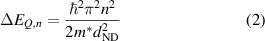
where n ⩾ 1 is the ordering number of the discrete level, m* the Si effective carrier mass, T the temperature;  the reduced Planck constant. To maintain the equidistant Coulomb oscillations as shown in figure 3, the energy difference between the ground state and the first level should exceed the value of the Coulomb blockade, that is

For Si NDs of approximately 3 nm in diameter (and even more for smaller ones), this condition is fulfilled as the bandgap widening for such QDs exceeds 0.5 eV [33].
In order to address the SET limitations, mainly the low current level (see figure 3(a)), its co-integration with a FET is favourable. The I–V characteristics of a hybrid SET/FET circuit (see figure 4(a)) proposed by [27] was simulated for a ND-SET/vNW-based FET configuration using BSIM-CMG models [34].

Figure 4. (a) Schematic of the hybrid SET-FET circuit; (b) IDS currents of the SET and the vNP-based hybrid SET-FET circuit. The inset illustrates the sub-threshold operation of the FET and the amplification of the Coulomb oscillations. For details, see [35]. Adapted from [35] CC BY 4.0 and [36] © IEEE. All rights reserved.
Download figure:
Standard image High-resolution imageAs shown in figure 4(b), the SET current is significantly amplified by six orders of magnitude by the FET operating at sub-threshold level.
The simulation tools and models also allow to study the influence of variations of CDs, such as tunnelling distances, the ND size or its lateral position, on the device characteristics. Results of such simulations were published in [35, 36]; some aspects with respect to experimentally observed deviations to targeted values are separately discussed in section 5.5 of this paper.
3. Simulation of Si ND formation in a confined oxide volume
The formation of Si NDs in Si rich oxides by thermally stimulated phase separation and Ostwald ripening has been demonstrated in numerous studies, for example [37–40] and references therein, a recent review paper [41] or also summarized in chapters 9–13 of the textbook 'Silicon Nanocrystals' [42] edited by Pavesi and Turan. The new aspect addressed in this work is to realize a single, self-assembled Si ND or only very few ones in the oxide of a vertically stacked Si/SiO2/Si pillar for SET applications. The basic approach to achieve this goal is to limit the volume of phase separation to a few hundreds of cubic nanometres, which corresponds well with the targeted volume of the oxide disc within the NP, as derived in the previous section.
Several techniques, including reactive magnetron sputtering, chemical vapour deposition and SiO evaporation, can be used to fabricate thin Si-rich oxide layers as matrices for subsequent phase separation. Here, we apply the method of ion-beam mixing at Si/SiO2 interfaces [43, 44] to enrich the initial stoichiometric SiO2 with Si. The excess Si content and its profile could be easily controlled by varying the irradiation fluence. Mixing of the Si/SiO2/Si stack is carried out by using chemically neutral Si ions at sufficiently high energy so that the ion penetration depth significantly exceeds the stack thickness.
For the synthesis of Si NDs within the oxide of a NP, two basic scenarios were considered. One option is to perform ion-beam mixing and subsequent annealing in pre-structured NPs. However, recent experiments revealed that RT ion irradiation at the required fluence deteriorates the stacked NPs by amorphization, leading to substantial NP shape changes during ion irradiation due to viscous flow of silicon [45]. This effect can be suppressed by performing ion irradiation at elevated temperatures (>400 °C), which preserves the crystalline morphology of the Si regions in the stacked NP. We discarded this option because most implantation tools in standard wafer process lines do not allow ion irradiation at temperatures above 400 °C. Alternatively, we decided to apply ion-beam mixing to a planar layer stack prior to electron-beam patterning and pillar etching. In this case, the volume of the mixed oxide disc is determined by the NP dimension after etching. Phase separation and ND formation are accomplished during subsequent annealing at temperatures up to 1100 °C which is viable owing to the high thermal and mechanical stability of the NPs.
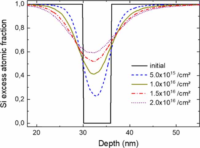
The modelling of this process sequence is accomplished in two steps, with dynamic collisional computer simulations of ion-induced atomic mixing using TRIDYN [46, 47] and subsequent kinetic Monte Carlo (kMC) simulations of the phase separation and ND formation. The accumulation of Si in the oxide interlayer during ion-beam mixing is illustrated in figure 5 which shows the depth profiles of excess Si in the oxide that develops under 50 keV Si+ irradiation. The Si excess atomic fraction is defined as [48]
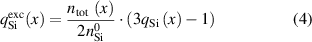
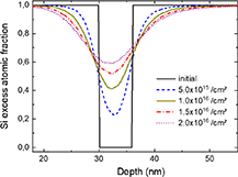
Figure 5. Si excess depth profiles in a planar 30 nm Si/6 nm SiO2/Si stack irradiated with 50 keV Si+ ions at different fluences, as obtained from TRIDYN computer simulation. The depth scale is individually corrected for the sputter loss of the outer Si layer, which is around 1 nm/1016 ions cm−2. For the definition of the Si excess atomic fraction, see equation (4).
Download figure:
Standard image High-resolution imagewhere ntot(x), nSi, qSi(x) denote the total (Si + O) atomic density, atomic density of crystalline Si (= 5 × 10²² at/cm3), and Si atomic fraction, respectively. For SiO2, SiO and pure Si,  amount to 0, 0.43 and 1, respectively. The profiles demonstrate significant ion-induced atomic mixing in the regions of both interfaces. The almost symmetric excess Si profiles in the oxide indicate a similar mixing efficiency at both interfaces, which is assured by the choice of the ion energy. In addition, there is a minor shift in the profile towards the surface which increases with increasing fluence. This is attributed to the deposition of implanted Si ions behind the oxide interlayer. (Note that the depth scales of figure 5 have already been corrected for surface erosion due to sputtering.)
The excess Si in the oxide continuously increases with the irradiation fluence, converting the initial SiO2 into an SiOx layer with a depth-dependent x value. As concluded from the subsequent kMC simulations, a stoichiometry of x ≈ 1 at the centre of the oxide layer optimizes the formation of well-separated Si NDs. This is achieved for a fluence of ∼1 × 1016 cm−2 which is a reasonable value with respect to the sputter loss of the upper Si layer (∼1 nm/1016 ions × cm−2) as well as the irradiation time (a few minutes). The maximum excess Si close to the oxide centre is beneficial for phase separation and Si ND formation. However, a recent study by Prüfer et al [49] showed that TRIDYN overestimates the interface broadening of the mixed Si profile, in particular for higher implantation fluences. This deviation is attributed to the neglect of chemical driving forces in connection with thermal-spike-induced diffusion during ion irradiation, which tends to reconstitute the Si/SiO2 interfaces. Accordingly, it is proposed to increase the fluence of the TRIDYN simulation by a scaling factor of ∼1.5 in the fluence range of interest [49]. Thus, an irradiation fluence of ∼1.5 × 1016 cm−2 appears to be appropriate for our purposes.
The excess Si depth profiles in the oxide (figure 5) were used as inputs for 3D kinetic Monte-Carlo simulations of phase separation and Si ND formation [50, 51]. Figure 6 shows a set of kMC simulations of Si ND formation after thermally driven SiOx → Si + SiO2 phase separation for stacked NPs of different diameters. It is evident that the number of precipitated Si NDs successively decreases towards lower pillar diameters. A single Si ND is formed for a strongly confined SiOx volume of approximately 500 nm3. For an oxide layer of 6 nm thickness, this volume corresponds to a NP diameter of about 10 nm.
Figure 6. Set of kMC simulations of SiOx phase separation and Si ND formation in cylindrical Si/SiOx /Si NPs of different diameters. The Si NDs projected in the front plane represent their number in the full oxide disc. The colour of the Si atoms represents its energy (blue: complete bonding in a diamond lattice, green:partly coordinated, red: dissolved as monomer in SiO2). The oxide is displayed transparent. The outer dashed lines are only introduced to mark the NP rim.
Download figure:
Standard image High-resolution imageThe vertical ND self-alignment almost at the oxide centre results from the symmetrical mixing effect at the upper and lower Si/SiO2 interfaces. The final Si NDs form with a size of 2–3 nm which agrees well with the preconditions for quantum confinement and RT operation of the SET, as set out in section 2. The very low diffusion coefficient of Si or SiO in the oxide enables small tunnelling distances and a sufficiently large thermal budget process window for the stable existence of Si NDs (see sections 5.1 and 5.5). The kMC simulations also reveal the recovery of smooth Si/SiO2 interfaces and a remarkable rounding of Si/SiO2 rims. The latter effect improves the electrostatic control of the ND and increases the drain-gate or source-gate breakdown stability.
4. Experimental
4.1. Process flow of NP/ND fabrication
Industrial, silicon wafer-level processes were employed on a front-end 200 mm CMOS line to ensure a high throughput and reproducibility of NP fabrication. The basic process flow is illustrated in figure 7 and mainly consists of the preparation of the planar layer stack, ion-beam mixing for SiOx formation, EBL for sub-100 nm patterning, multistep RIE using a hard mask for pillar fabrication and thermal processing for SiOx phase separation and Si ND formation. The final plasma oxidation step was used for NP shrinkage and gate oxide growth.
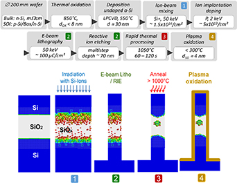
Figure 7. Processing scheme to fabricate stacked Si/SiO2/Si NPs with Si NDs embedded in the oxide. The key steps are sketched at the bottom.
Download figure:
Standard image High-resolution imageFor the experiments described here, mainly low-resistivity, n-type bulk-Si material was used. In parallel silicon-on-insulator (SOI) wafers with 200 nm top-Si and 400 nm buried oxide (BOX) necessary for the fabrication of integrated SET/FET devices were processed, too. The thickness of the thermal oxide was varied between 5 nm and 8 nm to optimize the Si ND size and tunnelling distances. As the top layer, undoped amorphous Si of 30 nm thickness was deposited by low-pressure chemical vapour deposition, and subsequently doped by low-energy phosphorous implantation. For ion-beam mixing, RT irradiations were performed using 50 keV Si+ ions at a fluence of 1.5 × 1016 cm−2 (i.e. with parameters as described in section 3) and at an angle of incidence of 7° with respect to the surface normal. For the subsequent dry RIE step the SOC/SiARC 5 layer stack acted as a hard mask. Isotropic resist trimming was additionally applied before etching to reduce the NP diameter. Details of this lithography/etching scheme were recently published by Pourteau et al [52]. The subsequent annealing step was performed using a rapid thermal processing (RTP) tool. A two-step sequence at 800 °C for 10 s followed by 1050 °C for 60 s or 120 s was applied. The intermediate annealing step at 800 °C was included to transform the amorphous top Si cap into poly-crystalline Si and to recrystallize the amorphous region in the bulk Si caused by ion-beam mixing. Generally, the heating rate was fixed at 25 K s−1, whereas the temperature profile during cooling followed an exponential decay as the wafers were not actively cooled. The necessity and details of the final plasma oxidation step are described in section 5.3.
To enable a systematic study of ND/NP fabrication and the reliability of lithography and etching steps, NPs of various size and with different distances were arranged in pillar arrays of 5 × 5 µm2 size each. Stand-alone NPs—so called isolated pillars—were processed in parallel. The nominal NP diameter (denoted as CD) was varied between 30 nm and 100 nm, whereas inter-pillar pitch distances between 60 nm and 1 µm (i.e. from 2× CD to 10× CD) were chosen. Several hundreds of such pillar arrays are regularly distributed across a wafer, enabling conclusions about the scalability of the technology and statistical variation of the CDs. More information regarding the lithography wafer layout is provided in the supplemental material S1 of this paper.
4.2. Structural characterization
Various state-of-the-art electron and ion microscopy techniques have been applied to the visualization and chemical analysis of nanostructures. In particular, structural characterization of the NPs and Si ND formation studies was carried out using an image-Cs-corrected Titan 80-300 transmission electron microscope equipped with a Gatan imaging filter Tridiem 863. While the NP dimensions can routinely be obtained using bright-field transmission electron microscopy (TEM), the detection of single Si NDs of 2–3 nm diameter inside an amorphous SiO2 matrix is challenging, because it requires likewise sufficient contrast (i.e. signal-to-noise ratio) and sub-nm resolution. Bright-field and annular dark-field TEM do not meet these two requirements, and high-resolution TEM can only map Si nanocrystals oriented in a low-index zone axis. Energy-filtered TEM (EFTEM), using the specific plasmon loss of Si or SiO2, was found to be the most appropriate method to enable a distinct contrast between Si and SiO2 and to image randomly oriented Si NDs in a SiO2 matrix [53]. EFTEM micrographs were recorded at energy loss windows of (17 ± 3) eV and (24 ± 2) eV corresponding to the Si and SiO2 plasmon losses, respectively. Most TEM images were obtained from cross-sectional specimens prepared by focused ion-beam thinning.
For imaging of an entire NP array (or parts of it), scanning electron microscopy (SEM) or helium ion microscopy (HIM) under tilted incidence conditions (typically 45°–60°) were applied. For SEM either a Helios NanoLab 1200HP or an NVision 40 were used, whereas HIM images were recorded with 25 keV helium ions in an ORION NanoFab instrument.
5. Results and discussion
5.1. Ion-beam mixing and SiOx phase separation
As derived in section 2, high-dose Si+ ion irradiation with a fluence of 1.5 × 1016 cm−2 is required to transform the initial SiO2 layer within the stack into SiOx (x ≈ 1). This fluence leads to the amorphization of the Si bulk below the oxide up to a depth of about 120 nm. Generally, this amorphization is uncritical as the substrate fully recrystallizes by epitaxial regrowth during subsequent RTP. When using SOI wafers, the top Si thickness must be larger than the amorphization depth to maintain a mono-crystalline seeding layer above the BOX for solid phase epitaxial regrowth.
An important issue for SET functionality is the quality of SiO2/Si interfaces which is influenced by the ion-beam mixing process. Figures 8(a)–(c) depicts a sequence of EFTEM micrographs showing the Si/oxide interfaces before and after irradiation and after annealing, respectively. As expected from the TRIDYN simulations (see figure 5), ion irradiation leads to blurring of the Si/oxide interfaces and an Si accumulation in the oxide from both sides. This is caused by the continuous mixing of Si into the oxide and oxygen into the adjacent Si regions. The subsequent annealing step (T > 1000 °C) provokes Si and SiO diffusion as well as phase separation, leading to Si ND formation and the recovery of Si/SiO2 interfaces [54, 55]. The relative Si depth profiles derived from line-scans of the Si-plasmon-loss-filtered TEM micrographs are shown in figure 8(d). They clearly reveal the mixing effect: the Si content in the oxide after mixing is significantly increased, and the still existing Si excess after annealing is caused by the presence of Si NDs which is indicated by the slight profile bump in the centre of the oxide. NDs are also seen as bright spots in figure 8(c). The strong recovery of the Si profile after annealing indicates that most of the excess Si condensates at Si/SiO2 interfaces during thermal treatment. The almost identical profile slopes of the as-deposited and annealed samples in figure 7(d) confirm the reconstitution of smooth interfaces after annealing.
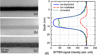
Figure 8. Sequence of Si-plasmon-loss-filtered TEM micrographs, showing the Si/SiO2 interface regions of an 30 nm a-Si/7 nm SiO2/bulk c-Si stack before (a) and after (b) ion irradiation as well as after annealing at 1050 °C for 60 s (c). Graph (d) displays normalized Si depth profiles as extracted from grey-scale values of EFTEM images (a)–(c) laterally averaged for regions of 15 nm width each. Note that this investigation has been carried out at a layer stack without NP patterning.
Download figure:
Standard image High-resolution imageThe parameters for the annealing step, required for phase separation and Si ND growth were investigated in detail by Xu et al [56] defining a thermal budget parameter TB
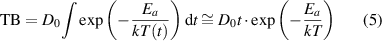
where D0 and Ea denote the diffusion coefficient and activation energy of the relevant SiO diffusion in SiO2, respectively (D0 = 4 × 104 cm2 s−1 and Ea = 6.2 eV) [54]. In the case of a negligible thermal budget during heating/cooling this equation has a simple exponential form, as shown on the right side of equation (5). Xu et al [56] determined a suitable process window of TB = (0.7–2.1) × 10−17 cm2 for the generation of Si NDs with a size of 2–3 nm. Although this study was performed for an unpatterned 2D layer stack, this TB value should also be a reasonable choice for the case of phase separation within the stacked NP considered here. The reason is the distinctly smaller distance of diffusing excess Si (or SiO) for condensation at both Si/SiO2 interfaces compared to the distance to the outer pillar rim. For the excess Si fraction close to the rim the situation might be different, but this finally only favours the formation of NDs in the NP centre which is a beneficial effect for single Si ND formation. Consequently, for the experiments described in this paper, RTP was usually carried out at 1050 °C and with times of 60 s or 120 s corresponding to TB = 0.6 × 10⁻¹⁷ cm2 or 1.1 × 10⁻¹⁷ cm2, respectively.
A critical issue is the proper choice of the annealing ambient. After annealing in pure nitrogen (grade 6.0) at 1050 °C, pitting at the pillar walls and pillar cap as well as at the bottom Si substrate bottom besides the NPs was observed (figure 9). These defects were not present directly after the NP etching before annealing. As a result of detailed investigations, excluding reasons such as thermally activated etching by halogen residuals from RIE, these defects are most probably caused by the formation of volatile SiO(g) from traces of humidity or oxygen in the annealing environment [57]. Options to circumvent this artefact are to use either an mixed N2/O2 atmosphere (oxygen content 1–2 vol.%) to favour sacrificial SiO2 layer formation or to protect the NP by a thin SiO2 film deposited prior to the RTP anneal, e.g. by low-temperature plasma-enhanced atomic-layer-deposition. In the latter case, post-annealing can be carried out in pure N2 atmosphere.
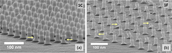
Figure 9. HIM micrographs of pillar arrays 1 C (a) and 1 F (b) after annealing at 1050 °C, 60 s in pure N2. NP dimension and pitch within the arrays are as follows: 1 C: 30 nm/90 nm: 1 F: 30 nm/210 nm. Critical features are marked by yellow arrows.
Download figure:
Standard image High-resolution imageBoth methods were successfully applied, yielding almost defect-free NP arrays, as shown in figure 10 for the case of annealing in N2/O2 mixed ambient. The oxide grown around the pillar with a thickness of (3 ± 1) nm (see figure 10(c)) is acceptable for further processing. The use of N2/1%O2 annealing is not detrimental to the formation of Si NDs in the centre of the oxide, as proven by EFTEM imaging (see figure 10(b)).
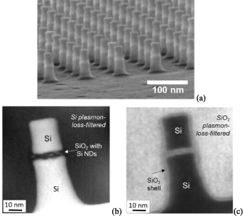
Figure 10. NPs after annealing in an N2/O2 = 99/1 vol.% atmosphere at 1050 °C for 60 s: (a) HIM image of an array with CD = 30 nm and a pitch of 90 nm × 90 nm, and (b), (c) EFTEM images of a single identical NP with Si-plasmon-loss (b) and SiO2-plasmon-loss (c) filtering. The formation of a few Si NDs in the oxide is confirmed in (b).
Download figure:
Standard image High-resolution imageA second advantage of using mixed N2/O2 atmosphere for RTP is the prevention of silicon-oxynitride formation at the outer Si NP rim which was confirmed by analytical TEM 6 after annealing at 1050 °C in pure N2. The Six Oy Nz films can only be removed by plasma or RIE dry etching with limited selectivity for other materials which is a critical issue for subsequent SET gate oxide formation and drain metallization.
5.2. NP morphology control
The device simulations in section 2 show that SET operation requires a final NP diameter of <12 nm. Therefore, NP arrays of various dimensions were investigated to determine the limits of the lithography/etching/annealing processes applied for the fabrication of defect-free NPs. Pillar arrays with CD = 30 nm and 60–300 nm pitch were of particular interest to elucidate pillar topology and the Si ND formation within the smallest NPs.
A first observation revealed that the NP diameter after RIE became a function of the NP pitch, as shown in figure 11(a). Note that resist trimming generally led to NP diameters smaller than the EBL designed CD values [52]. Starting from an NP diameter of about 28 nm, obtained for an array pitch of 60 nm, it shrinks with increasing pitch down to a diameter of 17 nm. Above 200 nm pitch, the shrinkage saturation represents the situation of stand-alone pillars. This shrinkage effect was caused by the simplified lithographic workflow at which electron-beam proximity correction was not applied before exposure of negative EBL resist. This results in overexposed patterns at small pitch values due to locally scattered electrons. As a second effect, a reduction in the oxide layer thickness for decreasing NP diameters was observed (figure 11(b)). The thickness reduction can be explained by the charging of the NP cap during the final phase of pillar etching, leaving the upper Si-cap electrically isolated. This charging leads to local breakdowns and SiO emanation at the rim of the oxide [58]. The easiest option to compensate for this oxide shrinkage is to increase the initial oxide thickness within the stack. Another technical option is the isolation of the entire wafer during RIE.
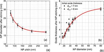
Figure 11. (a) NP diameter for pillars of array 1 (CD30) after RIE and subsequent RTA (1050 °C, 60 s, N2/O2 = 99/1 vol.%), (b) reduction of the intermediate oxide thickness after RIE for stacked Si/SiO2/Si pillars of various diameters and ∼80 nm total height.
Download figure:
Standard image High-resolution imageThe investigations described so far show that sub-30 nm NPs can be realized by direct EBL and RIE etching. However, the yield of defect-free pillars rapidly decreased to <50% for stand-alone NPs less than 20 nm in diameter. Main artefacts are the removal of the top Si cap, NP bending, or a strong trapezoidal shape of the stacked pillars.
5.3. NP shrinkage technology
As a consequence of the yield drop of sub-20 nm diameter NPs after RIE, an additional process step is necessary to shrink the NP size from ∼20 nm to the targeted diameter of <12 nm. A common technique for reducing the size of Si nanostructures is sacrificial oxidation [59, 60]. Usually by thermal oxidation, the surface of the Si nanostructure is oxidized with consumes a Si layer of dSi = 0.44⋅dox thickness by conversion into SiO2. This oxide layer can be selectively removed by hydrofluoric acid (HF), resulting in a reduction of the initial nanostructure dimension. Accordingly, the NP diameter reduction was tested using rapid thermal oxidation at temperatures between 850 °C and 1050 °C. However, a closer look at NPs with an initial diameter of <20 nm by EFTEM showed the dissolution of the existing Si NDs during this treatment, which is attributed to Si ND oxidation 7 . This can be avoided using the microwave-based plasma oxidation technique operating at temperatures <400 °C [61, 62]. Plasma oxidation provides oxides of up to ∼8 nm in thickness and high electrical quality [63, 64] at reasonable oxidation times of some minutes. In collaboration with the company HQ Dielectrics GmbH (HQ-D), experiments were carried out with the HQ-D HyperionLT tool [65] (suitable for processing up to ⊘ 300 mm wafers) to qualify the plasma process for the oxidation of NPs. The oxidation was performed in a microwave plasma (2.45 GHz) using O2/He gas ratio of 85/15 vol.%, a working pressure of about 35 Pa and a power density of 2 W cm−2.
Figure 12 shows the uniform oxidation of NPs and the preservation of the Si NDs after plasma oxidation. Remarkably, the thickness of the intermediate oxide layer in the Si/SiO2/Si sandwich did not change. Limiting the processing temperature to <350 °C and staying within the linear oxidation regime, an oxide layer up to 6 nm thickness around the NP can be realized. This corresponds to an NP diameter shrinkage of approximately 5 nm per oxidation cycle. As the procedure can be repeated after removing the oxide by HF, NPs with a final diameter of <12 nm can be obtained by single or multiple plasma oxidation, depending on the initial NP diameter. Plasma oxidation technology provides another advantage: it can also be used to grow the gate oxide required for a GAA SET (see figures 2 and 7). A breakdown field >10 MV cm−1 was measured at planar MOS structures for a gate oxide of 3 nm thickness produced by plasma oxidation.
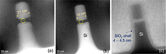
Figure 12. Si-plasmon-loss-filtered EFTEM images before (a) and after (b) a single plasma oxidation (He/O2 = 85/15 vol%, 35 Pa, 2 W cm−2) for 90 s (250 °C max.). The initial 20 nm NP diameter reduces to 16 nm. The EFTEM image after plasma processing (b) confirms the existence of a Si ND (marked by a yellow circle). (c) SiO2-plasmon-loss-filtered EFTEM image of the pillar shown in (b) confirming the uniform formation of an ∼4.2 nm oxide around the NP.
Download figure:
Standard image High-resolution image5.4. Towards a single Si ND
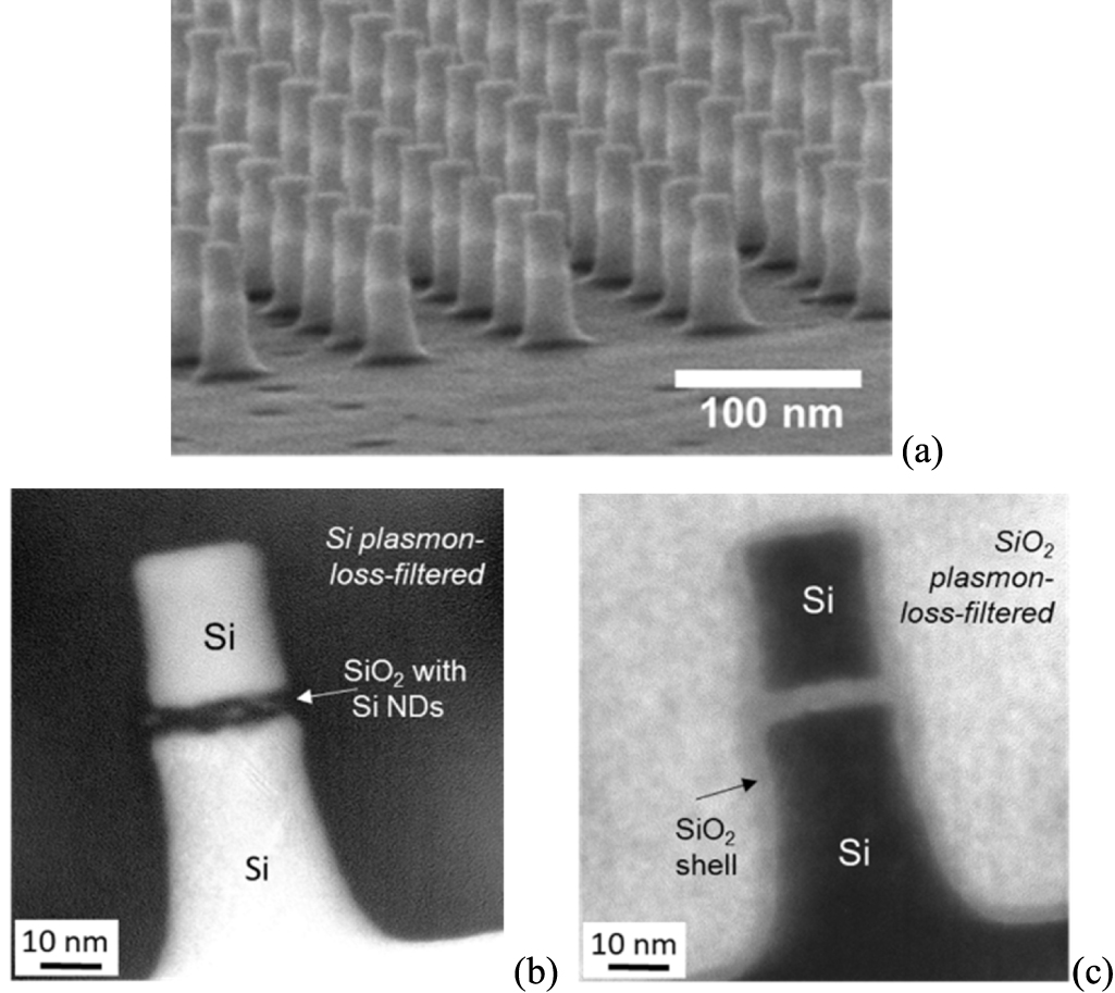
Figure 13 depicts a sequence of EFTEM images of isolated NPs with diameters varying between 35 nm and 18 nm, which were fabricated from the same layer stack of Si (30 nm)/SiO2 (6 nm)/Si under identical ion-beam mixing, pillar etching and annealing conditions. The corresponding NP/ND features are summarized in table 1.
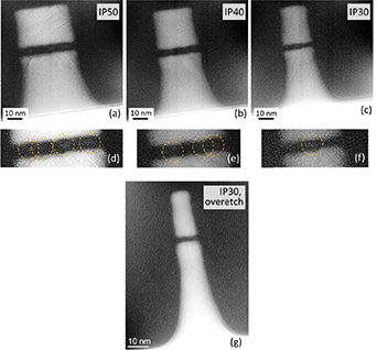
Figure 13. (a)–(c): Si-plasmon-loss-filtered EFTEM micrographs showing isolated NPs (IPs) of nominal 50 nm, 40 nm, and 30 nm diameter, fabricated from an identical stack of 30 nm Si/6 nm SiO2/Si by the process flow sketched in figure 7. The enlarged details (d)–(f) show the oxide region with Si inclusions marked by yellow rings. The image (g) shows an IP30 pillar fabricated by RIE over-etching which leads to a deeper pillar base below the oxide. This results to a smaller pillar diameter, but the oxide thickness is also reduced to 3 nm.
Download figure:
Standard image High-resolution imageTable 1. Values for the effective NP diameter dNP, the oxide thickness dox and number of NDs in the pillars of figure 13 including also the cases IP45 and IP35 not shown there.
| Parameter | Unit | IP50 | IP45 | IP40 | IP35 | IP30 | IP30,oe |
|---|---|---|---|---|---|---|---|
| dNP | nm | 37,0 | 33,0 | 27,5 | 21,7 | 18,6 | 10,5 |
| dox | nm | 5,6 | 5,4 | 4,8 | 4,2 | 3,8 | 3,0 |
| # NDs (min) | 3–4 | 3 | 3 | 2 | 1–2 | 0 | |
| Figure 11 | (a), (d) | (b), (e) | (d), (f) | (g) |
The number of Si NDs decreases with decreasing NP diameter, which is in close agreement with kMC simulations (see figure 6). In most pillars Si precipitates could be detected, except for an oxide thickness of ⩽3 nm. In this case the oxide is too thin to generate a Si ND of 2–3 nm as it immediately dissolves by de-wetting if touching the Si/SiO2 interface.
Considering all aspects described before, we successfully produced stacked Si/SiO2/Si NPs <12 nm in diameter with a single Si ND embedded in the oxide. This is illustrated in figure 14, which shows the EFTEM image of a NP of (11 ± 1) nm diameter with a single Si ND in the centre of the 3.7 nm thin SiO2 disc formed by the self-organization and self-alignment mechanisms discussed in section 3. The ND has a diameter of 2.5 nm, the tunnelling widths on both sides are ⩽1.2 nm which suggests the ability for SET operation at RT.
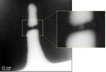
Figure 14. EFTEM (Si-plasmon-loss-filtered) image of a NP of about 11 nm in diameter with a single Si ND embedded in the centre of the thin 3.7 nm thin oxide. The enlarged detail on the right confirms a size of the almost spherical Si ND of 2.5 nm and tunnelling distances to neighboured Si regions of about 1 nm.
Download figure:
Standard image High-resolution imageThe widening of the oxide layer at the pillar rim is in agreement with the targeted layout and predictions by kMC simulations (see figure 6), which is advantageous for the reduction of the electrical field strength at the gate region. The results provide a proof of the manufacturability of vertically stacked NPs with embedded Si NDs and reveal that tunnelling distances close to 1 nm can be achieved.
5.5. Impact of NP/ND parameter variations
The NP/ND manufacturing process at sub-20 nm level described in previous sections and the statistical nature of SiOx phase separation and Si ND formation results in some variations of the number of Si NDs as well as their size and lateral position in the oxide. Because of the strong geometrical constraints in the NP, these variations are generally small. It is outside the scope of this paper to discuss this matter in detail here (see [35, 36]), but let us briefly consider four experimentally observed situations with their consequences for SET or SET/FET operation and possible options to balance such variations.
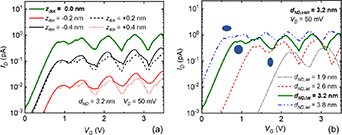
- i.The tunnelling transmission coefficient exponentially depends on the tunnelling distance. Thus, the most critical parameter is a very thin tunnel distance dT of about 1 nm to achieve SET currents in the pA range (see figure 3). A variation of 10% in the tunnelling thickness will change the SET current by one order of magnitude [35]. For the hybride SET/FET circuit such a variation modifies the FET drain-source current by 20% [35, 36]. Any asymmetry of the upper/lower tunnelling distances will also considerably lower the SET current, as shown in figure 15(a). It is an essential issue to reduce and to unify the tunnelling distances. The very low diffusion coefficient of Si or SiO in SiO2 (D ≈ 10−21 cm2 s−1 @ 1050 °C, see [54, 66]) implies a low diffusional screening length which is essential to enable tunnelling distances of about 1 nm or even slightly below (see figure 14). Thus, for a reduced oxide thickness one can expect a stronger localization of Si NDs with respect to both Si/SiO2 interfaces and the unification of tunnelling distances.
- ii.Simulations reveal that the ND shape (spherical, elliptical or elongated) has only a minor influence on the SET current as shown in figure 15(b). Flattened NDs, which is the most observed variation in the ND shape due the vertical confinement, requires lower VG voltages. The SET current is almost constant as long as the tunnelling distances remain small enough and as long the conditions of equations (1) and (3) are still fulfilled.
- iii.Furthermore, the lateral position of a single Si ND may deviate from the oxide centre. This increases the gate-dot capacitance CGD and slightly lowers VG which is beneficial for SET operation.
- iv.It is also observed that more than one (typically 2–3) NDs form, particularly for larger NPs of >15 nm diameter. Within a small ensemble of NDs the tunnelling distances will not exactly be identical which has a strong impact on the SET current. Consequently, a self-selection of a specific ND characterized by the lowest tunnel barrier will happen. Moreover, there is also a technological way to favour a single, centred Si ND. It has been experimentally shown (see supplemental material S3) that annealing in a strongly diluted N2/O2 ambient dissolves Si NDs close to the rim of the NP while preserving near-centred NDs. Optimization of the oxygen content in the annealing ambient and the thermal budget will favour the formation of single NDs in cases that the NP dimension exceeds the 10 nm diameter level.
Figure 15. Influence of a vertically asymmetric ND position (a) or a laterally shaped ND on the SET current (b). Fixed parameters are dOX = 5.6 nm, dNC= 10 nm; dND = 3.2 nm and VD = 50 mn.
Download figure:
Standard image High-resolution image
In addition to process developments mentioned before, there is also another option to balance NP/ND topological variations. Both, SET and FET devices present a vertical topology with high integration capability. This entails the possibility to implement SET arrays connected in parallel that can suppress the variability impact [67]. However, further efforts are necessary to reduce the variations in order to achieve a higher technology readiness level.
6. Summary and further work
This paper describes the CMOS-compatible fabrication of Si/SiO2/Si NPs with embedded Si NDs suitable as key functional elements for a quantum-dot-based, GAA SET. Remarkably, all process steps were carried out using industrial equipment on ⊘ 200 mm bulk Si or SOI wafers, which confirms the manufacturability of the NP/ND structures in a complex wafer flow at a large wafer level.
To realize the ND/NP structures, a novel process flow that combines bottom-up and top-down technologies has been developed. Geometrical constraints and technological process parameters have been derived partly from predictive physical processes and device simulations, partly by using our experimental experience related to the formation of near-interface Si NDs. Finally, the reliable formation of Si NDs < 3 nm in the oxide of a stacked Si/SiO2/Si NP ⩽ 12 nm in diameter with tunnelling distances of approximately 1 nm between the Si ND and the adjacent Si regions could be demonstrated. The impact of CD variations on the SET properties has been analysed by device simulations. Well defined, symmetric and ultra-thin tunnelling distances (∼1 nm) have the strongest influence on the SET current. Deviations in the shape of the NDs or their lateral position in the pillar are of less importance. Layout and technological options were discussed to suppress deviations for further improvements.
The work gained at physico-chemical understanding of the self-organization and patterning of nanostructures. This involves processes like ion-beam mixing, phase separation, reactive ion etching or plasma oxidation which might be helpful for future processing in nanoelectronics in general. In particular, the experimental verification of the predicted self-assembly of single Si NDs by phase separation within a confined SiOx volume of <500 nm3 and the ability to locate such self-assembled QDs within a direct tunnelling distance to a Si electrode is highly relevant for nanoelectronics.
This study limits on the fabrication and structural characterization of NPs/NDs as key functional elements for the SET. In the Ions4SET project [68] further work was carried out to fabricate and electrically characterize NPs with Si NDs and single SETs [69]. Moreover, the entire integration schema for a hybrid SET/FET device was elaborated and tested [30]. An important issue was to verify that the NPs/NDs could withstand the thermal, mechanical and chemical stresses of a complex SET/FET fabrication flow. These investigations reveal that the NPs/NDs maintained their stability during the entire process, if they are embedded in sacrificial Si3N4 dielectrics and if the thermal budget during FET processing is limited to 900 °C/3 h, which are acceptable preconditions for state-of-the-art transistor technology.
Acknowledgments
This work received funding from the European Union's Horizon 2020 Research and Innovation Program under Grant Agreement No. 688072 (Project acronym: Ions4SET), which is gratefully acknowledged. The authors thank the Ions4SET Industry Endorsement Board for their continuous support during the project. In particular, the valuable inputs of K-H Stegemann (XFAB Dresden GmbH) was very helpful in developing the process flow for ND/NP fabrication and in solving several critical issues related to the processing of nanostructures. The authors thank W Lerch and J Niess from HQ Dielectrics GmbH (HQ-D) for providing and performing plasma oxidation at the HQD HyperionLT tool and their efforts to qualify this technique for the shrinkage of NPs. Numerous test preparations and extensive analytical work were carried out at the Ion Beam Center (IBC) and the Nanofabrication Facilities Rossendorf (NanoFaRo) at HZDR which is gratefully acknowledged.
Data availability statement
The data that support the findings of this study are available upon reasonable request from the authors.
Conflicts of interest
The authors declare no conflicts of interest. We certify that the paper is an original work, approved by all co-authors, and not published elsewhere. The study is in agreement with the 'DFG rules for good scientific practice' which complies ethics in science.
Footnotes
- 5
SOC: Spin-On-Carbon; SiARC: Silicon-Anti-Reflective Coating
- 6
See supplemental material S2 for detailed information.
- 7
See supplemental material S3 for detailed information.
Supplementary data (0.8 MB PDF)