

Abstract
The radiation effect of swift heavy ions (16 MeV 181Ta) on the Au/Ni/β-Ga2O3 vertical Schottky barrier diodes (SBDs) were investigated at the fluence of 1 × 10⁸, 3 × 10⁸ and 3 × 109 cm−2. The SBDs were characterized by current density–voltage (J–V) and capacitance–voltage (C–V) measurements. It was found that Schottky barrier height φ decreased from 1.11 eV to 0.94 eV, the ideality factor n increased from 1.01 to 1.29, turn-on voltage Von increased from 0.52 V to 0.80 V after radiation of 3 × 109 cm−2. The reverse breakdown voltage was decreased from −405 V to −375 V, −350 V and −255 V after radiation of 1 × 10⁸, 3 × 10⁸ and 3 × 109 cm−2, respectively. In addition, the carrier concentration calculated from the capacitance–voltage curves was decreased significantly. Based on the G/ω–ω measurement results, the trap density at the Ni/β-Ga2O3 interface was extracted to be 2.89 × 10¹⁵–2.49 × 1016 cm−2 eV−1 and 2.18 × 10¹⁵–4.98 × 1016 cm−2 eV−1 with the energy level of 0.85–0.87 eV below the conduction band edge.
Export citation and abstract BibTeX RIS
1. Introduction
Ga2O3 crystals exhibit polymorphism with five confirmed polytypes (α, β, γ, δ,  ). β-Ga2O3 is believed to be the most stable and, hence, the most extensively used phase [1, 2]. β-Gallium oxide has emerged as a promising material for power electronics, owing to superior material properties such as an ultrawide bandgap of 4.9 eV and a high breakdown electric field of up to 8 MV cm−1 [3], which enable β-Ga2O3 based devices to operate at high temperature and high voltage bias [4]. Another important advantage of β-Ga2O3 is that large, high-quality bulk single crystals can be grown by melt growth methods [5–8]. Furthermore, various types of devices, including Schottky barrier diodes (SBDs), metal-oxide-semiconductor field effect transistors and solar-blind photodetectors have been fabricated and the device characteristics carefully investigated. Since the expected application of β-Ga2O3 devices in artificial satellites, launch vehicles, and spacecraft, there are much interests in their ability to withstand high radiation fluences consisting of high-energy protons, electrons, neutrons, gamma rays, and heavy ions (HIs) [9, 10].
These particles produce various effects on semiconductor devices, including the accumulation of ionizing dose deposition over a long period, known as the total ionizing dose effect and the accumulation of non-ionizing dose deposition due to lattice defects generated by protons or high energy electrons, leading to displacement damage (DD) effects [11, 12]. Although some effects of proton, electron, gamma ray and neutron irradiation on β-Ga2O3 material and device properties have been reported recently, there is few investigations of the influence of HIs irradiation on β-Ga2O3 SBDs [13]. In 2020, Chen et al reported for the first time the influence of x-ray irradiation under bias voltage on the field effect transistors prepared by mechanically stripped β-Ga2O3 nano strips [14]. In 2022, N. Manikanthababu et al reported the situ electrical characteristics and defect dynamics induced by swift HI irradiation of 120 MeV Au9+ in a fluence range of 1 × 10¹⁰–2 × 10¹² ions cm−2 in Pt/PtOx /β-Ga2O3 vertical SBDs [15].
In this paper, we reported the effects of swift HIs (16 MeV 181Ta) radiation on vertical β-Ga2O3 Schottky diodes under the fluence of 1 × 10⁸, 3 × 10⁸ and 3 × 109 cm−2. The trap densities introduced at the Au/Ni/β-Ga2O3 interface were extracted to be 2.89 × 10¹⁵–2.49 × 1016 cm−2 eV−1and 2.18 × 10¹⁵–4.98 × 1016 cm−2 eV−1 for 1 × 10⁸ and 3 × 108 cm−2, respectively, with the trap energy of 0.85–0.87 eV below the conduction band edge.
2. Device fabrication
Figure 1 presents the schematic cross section of β-Ga2O3 SBD. The β-Ga2O3 drift layer with a n− doping concentration of 1 × 1017 cm−3 and thickness of 8 μm was grown on the β-Ga2O3 substrate with n+ doping concentration of 1 × 1018 cm−3 by hydride vapor phase epitaxy, which was purchased from Novel Crystal Technology, Inc. After ultrasonic cleaning in acetone, ethanol and deionized water for 10 min, respectively, the metal stack of Ti (60 nm)/Au (120 nm) was deposited on the backside of β-Ga2O3 drift layer by e-beam deposition, then thermal annealed at 500 °C for 60 s to reduce ohmic contact resistance. Schottky Ni (50 nm)/Au (80 nm) circular contacts with the diameter of 100 μm were deposited using e-beam evaporation.
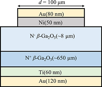
Figure 1. The schematic cross section of β-Ga2O3 SBD.
Download figure:
Standard image High-resolution imageThe HIs irradiation was performed using the Heavy Ion Research Facility in Lanzhou at the Institute of Modern Physics, Chinese Academy of Sciences. Samples were irradiated by 16 MeV u−1 181Ta ions beam with fluences of 1 × 108 cm−2, 3 × 108 cm−2 and 3 × 109 cm−2 (labeled as sample A, sample B and sample C) at room temperature, and the beam spot size was 4 cm × 4 cm.
The forward current density–voltage (JF –V), reverse current density–voltage (JR –V), and high-frequency capacitance–voltage (C–V) characteristics were measured by Keithley 4200A-SCS and Agilent B1500A semiconductor parameter analyzers. The frequency-dependent conductance measurement (G–ω) was performed to evaluate the interface states density introduced by irradiation. In addition, the Ta ions transportation process was simulated by the stopping and range of ions in matter (SRIM) software and the device characteristics were also simulated by Sentaurus with the average vacancies density calculated from SRIM and the trap level extracted by G–ω used in the model.
3. Result and discussion
Figure 2(a) shows the SRIM simulation result of 16 MeV Ta ions irradiation in β-Ga2O3 SBD. Ta ions transferred energy to Ga atoms and O atoms in β-Ga2O3 along their incident path, and deposited their own energy in the target material with the slowdown process after ions incidence. Generally, there are two energy loss mechanisms before the incident ions' energy are completely lost. One is named electron energy loss (Se), which means that high-energy incident ions transfer energy to electrons to excite or ionize electrons. The other is named nuclear energy loss (Sn), which means the elastic collision of ions with atoms during ions incidence, resulting in vacancies, interstitial atoms and Frenkel defects, etc. In this simulation, the depth of 16 MeV Ta ions in the device was about 2.51 µm, and thus, ions would not stop at the interface between the metal stack (Au/Ni) and the semiconductor (β-Ga2O3) but reach the drift layer instead. As the incident ions entered the drift layer, Se decreased while Sn increased with the increase of the incident depth and Se (7.08 KeV nm−1) was 10 times that of Sn (0.67 KeV nm−1). The dominant energy loss mechanism was Se in the whole range of radiation damage, which excited or ionized electrons and induced deep defect levels. These defects served as the trap centers, deteriorating the electrical performance of the β-Ga2O3 SBD,

Figure 2. The distribution diagram of (a) Se and Sn (b) vacancies generated by 16 MeV Ta ions irradiation in β-Ga2O3 SBD from the SRIM simulation.
Download figure:
Standard image High-resolution imageThe vacancy densities produced in β-Ga2O3 SBD irradiated by a single Ta ion of 16 MeV is shown in figure 2(b). The average value is 1.57/Å-ion. According to equation (1), the average vacancy densities, determined by SRIM simulation were 1.57 × 10¹⁶, 4.71 × 10¹⁶ and 4.71 × 1017 cm−3 for three samples after radiation, which were included in the Sentaurus model to analyze the influence on the electrical characteristics of SBD with the trap energy of ∼0.85 eV below the conduction band edge (described in the following).
Figure 3 shows the measurement and simulation results of forward J–V curves for three samples before and after 1 × 108 cm−2, 3 × 108 cm−2 and 3 × 109 cm−2 16 MeV u−1 181Ta irradiation. The simulation results were in good agreement with the experiment. With the increase of the irradiation dose, the current density decreased monotonously as the bias larger than turn-on voltage of 0.52 V (defined as the voltage @J= 10−3 A cm−2). At the forward bias of 5 V, the current density remains almost constant for sample A and decreased from 1216.3 A cm−2 to 1027.1 A cm−2 for sample B. However, for sample C, the forward current density was seriously decreased to 0.19 A cm−2 and the device performance was deteriorated significantly.

Figure 3. The forward J–V curves from (a) experiments and (b) simulations of β-Ga2O3 before and after Ta ions radiation for three samples.
Download figure:
Standard image High-resolution imageAssuming standard thermionic emission (TE) theory, the forward current density can be expressed in the following form [16]
where J is the current density, T the absolute temperature, q = 1.6 × 10⁻¹⁹ C is electron charge, k0 the Boltzmann constant, and n the ideality factor representing the difference between the experimental Schottky diode and the ideal Schottky diode, Js the reverse saturation current density, φ the Schottky barrier height, A* is the Richardson constant of 41 A cm−2 K−2 [17].
Figure 4(a) presents the lnJ–V curves before and after radiation for three samples, respectively. The linear part of the lnJ–V curves was taken for fitting to extract n and φ, as shown in figures 4(d) and (c). For the radiation doses of 1 × 108 cm−2 and 3 × 108 cm−2, the n and φ remain almost constant, about 1.01–1.03 and 1.08–1.11 eV. When the radiation dose increasing to 3 × 109 cm−2, φ decreased from 1.11 eV to 0.94 eV and n increased from 1.01 to 1.29, illustrating that the TE was the dominant transport mechanism but the trap-assisted tunneling and the field emission were also involved, which may be related to the introduction of trap centers at (Au/Ni)/β-Ga2O3 interface and the defects formation in the epilayer during Ta ions radiation [18]. When a large number of Ta ions reached the (Au/Ni)/β-Ga2O3 interface, much more atoms would be ionized and act as trap centers to increase the electric field at the interface, leading to the decrease of Schottky barrier height [18]. In addition, the defects also could be formed along the incident path in the β-Ga2O3 epilayer and introduce energy levels in the bandgap, enhancing the electron tunneling and the higher n. On the other hand, after radiation, the turn-on voltage (Von) increased from 0.52 V to 0.54 V, 0.56 V and 0.80 V for three samples, respectively.

Figure 4. (a) The lnJ–V curves. (b) Von (c) φ and (d) n as a function of radiation fluence before and after irradiation for three samples.
Download figure:
Standard image High-resolution imageFigure 5 shows the variation of the differential resistance with the forward bias for three samples before and after radiation. For sample A and B, the on-resistance (Ron) were 3.14 Ω cm2 and 3.51 Ω cm2 after radiation, which only has slight increment compared to the value of 2.73 Ω cm2 before radiation. With the radiation dose of 3 × 109 cm−2, Ron significantly increased from 2.73 Ω cm2 to 5.0 × 10⁴ Ω cm2, which may be attributed to the DDs generated in β-Ga2O3 film after irradiation and the substantial decrease in carrier concentration and mobility [19].
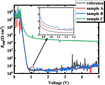
Figure 5. The differential on-resistance before and after irradiation for three samples.
Download figure:
Standard image High-resolution imageFigure 6(a) depicts the reverse J–V curves of β-Ga2O3 SBD before and after 1 × 108 cm−2, 3 × 108 cm−2 and 3 × 109 cm−2 16 MeV u−1 181Ta irradiation. The reverse current (IR) of β-Ga2O3 SBD increased with the irradiation dose until the device broke down. The breakdown voltage was decreased from −405 V to −375 V, −350 V and −255 V for three samples, respectively. The simulation results were also presented in figure 6(b), In addition to the Shockley–Read–Hall, Auger recombination and field-dependent mobility model [20], the tunnel mode was also included in the simulation process with the deep acceptor energy level of EC-0.85 eV (extracted by G–ω curves in the following) and the concentration of 1.57 × 10¹⁶, 4.71 × 10¹⁶ and 4.71 × 1017 cm−3 (the average vacancy densities determined by SRIM simulation in the above). The simulation results were in coincidence with the experiment data. As shown in figure 6(b), at −250 V, IR increased to 5.8 × 10⁻² A cm−2 for sample C after radiation with a dose of 3 × 109 cm−2, about three orders of magnitude higher than that before irradiation. This phenomena can be explained as the following, with φ decreasing from 1.11 eV to 0.94 eV for sample C, the reverse saturation current density is 5.8 × 10⁻² A cm−2, much higher than 3.0 × 10⁻⁵ A cm−2 before radiation and resulting in the reverse leakage current increase. In addition, much electrons tunneling from anode to cathode through the interface states at (Au/Ni)/β-Ga2O3 interface leading to the increase of reverse leakage current.

Figure 6. The reverse J–V curves from (a) experiments and (b) simulations of β-Ga2O3 SBD for fluences of 1 × 108 cm−2 (sample A), 3 × 108 cm−2 (sample B), and 3 × 109 cm−2 (sample C) before and after irradiation.
Download figure:
Standard image High-resolution imageFigure 7 presents the high frequency (1 MHz) C–V curves and 1/C2 –V curves at the AC frequency of 1 MHz of three samples before and after Ta ion radiation. The C–V relationship for a Schottky barrier is [21]
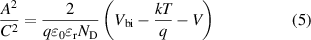
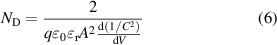

Figure 7. The C–V curves and 1/C2 –V curves (1 MHz) for three samples before and after Ta ion radiation. (c) Extracted carrier concentration of three representative samples.
Download figure:
Standard image High-resolution imagewhere, 0 = 8.85 × 10⁻¹² F m−1 is the vacuum dielectric constant, r = 10 is the relative permittivity of β-Ga2O3, ND is the electron concentration of the drift layer, Vbi is the built-in potential, and A (πr2, r= 50 μm) is the area of SBD. The electron concentration Nd of β-Ga2O3 drift layer could be determined by the slope of the 1/C2
–V curve, 4.92 × 1017 cm−3 before radiation and 3.41 × 1017 cm−3 for sample A, 2.91 × 017 cm−3 for sample B, respectively. The electron concentration decreased by 30% (sample A) and 40% (sample B) after radiation. Moreover, we have obtained a doping profile (concentration versus depth) as shown in figure 7(c). Thus, we assumed that during Ta ion irradiation, the defects introduced in the β-Ga2O3 drift layer could act as deep acceptor traps to capture electrons and the carrier concentration was decreased, space charge region widened and the capacitance was also reduced. However, as the radiation dose further increasing to 3 × 109 cm−2, a large number of defects were introduced that the electrical conductivity of the β-Ga2O3 epitaxial layer dramatically fell down. The variation of capacitance with bias could not be obtained, as shown in figure 7(b). Furthermore, the carrier removal rate (RC) was calculated to be 1.5 × 109 cm−1 and 6.7 × 108 cm−1 for sample A and sample B, respectively. RC increased rapidly after low-dose irradiation (sample A), when the irradiation dose was further increased (sample B), RC decreased for the most of the carriers in the drift layer had been removed by low-dose irradiation and the number of carriers that could be removed was limited and RC no longer increased.
As shown in figure 8, the frequency dependent C–V curves were obtained for sample A and sample B after radiation. The capacitance changed slowly at low voltage, then increased rapidly to reach the peak capacitance at bias voltage of 0.7 V. During radiation, the high energy ions broke the atomic bonds at the metal–semiconductor interface easily and a large number of interface states were generated, capturing and releasing carriers with the bias and additional interface state capacitance was introduced [22]. At low frequencies, most of the interface states could follow the AC voltage and a high capacitance was achieved. As the frequency further increasing, the interface states could not follow the change of the AC voltage, and the capacitance gradually decreased.

Figure 8. The frequency dependent C–V curves for (a)sample A (b) sample B after Ta ion radiation.
Download figure:
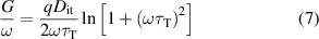
Standard image High-resolution imageMoreover, the frequency dependent conductance measurements were employed to characterize the interface state at the metal-semiconductor contact interface, as shown in figure 9. If we assumed that the energy of the trap was continuously distributed in the whole β-Ga2O3 forbidden band, the equivalent parallel interface trap conductance G/ω and the trap energy below the conduction band ET could be expressed as [23]


Figure 9. The G/ω–ω curves under different bias voltages for (a) sample A (b) sample B.
Download figure:
Standard image High-resolution image
where Dit, τT and ω are the trap density, time constant and the radio frequency. σT = 1 × 10⁻¹⁵ cm2 is the trapping cross section of the trap state [24], NC = 5.2 × 1018 cm−3 is the density of states in the conduction band [25], νt = (3 kT m−1 *)1/2 is the average thermal velocity of carriers, m* = 0.28m0 is the effective mass of electrons [26]. According to equations (7) and (8), Dit, τT and ET were determined for sample A and B after radiation. The interface trap density was about 2.89 × 10¹⁵–2.49 × 1016 cm−2 eV−1 and 2.18 × 10¹⁵–4.98 × 1016 cm−2 eV−1 with the energy level of 0.85–0.87 eV below the conduction band edge for sample A and B, respectively.
4. Conclusion
In this work, Au/Ni/β-Ga2O3 vertical SBDs were fabricated and irradiated with swift HIs (16 MeV 181Ta) at the ion fluence of 1 × 10⁸, 3 × 10⁸ and 3 × 10⁹ ions cm−2. With the radiation dose of 3 × 109 cm−2, φ decreased from 1.11 eV to 1.05 eV and n increased from 1 to 1.35. The breakdown voltage was decreased from −405 V to −375 V, −350 V and −255 V, respectively. The C–V measurement results indicated that irradiation introduced acceptor defects at interface and in the drift layer, trapping carriers and reducing the carrier concentration of the epitaxial layer. The trap density at the Ni/β-Ga2O3 interface were extracted to be 2.89 × 10¹⁵–2.49 × 1016 cm−2 eV−1 and 2.18 × 10¹⁵–4.98 × 1016 cm−2 eV−1 with the energy level of 0.85–0.87 eV below the conduction band edge for sample A and B, respectively.
Our results indicate that Au/Ni/β-Ga2O3 vertical SBDs has an intrinsically low susceptibility to radiation-induced material degradation. However, it will still have a negative effect on the characteristics of the Schottky junction and, hence, the performance and reliability of β-Ga2O3-based high power rectifiers, metal-semiconductor field effect transistor (MESFETs) and high electron mobility transistor (HFETs) operating in high-energy radiation environments.
Acknowledgments
This work was supported by the National Natural Science Foundation of China (NSFC) under Grant Nos. U21A20503, 61974112 and 61974115.
Data availability statement
The data that support the findings of this study are available from the corresponding author upon reasonable request.
The data that support the findings of this study are available upon reasonable request from the authors.