
Abstract
We report on the fabrication and electro-optical performance of ridge waveguide (RW) lasers emitting near 905 nm based on a vertical layer structure consisting of three single quantum wells (SQWs) as active regions separated by two tunnel junctions (TJs). The single waveguide core is designed in such a way that the third vertical mode is lasing. The width of the ridge is varied between 3 µm and 200 µm. Deep- and shallow-etched ridges were fabricated. The shallow etching stopped slightly above the topmost SQW, whereas the deep etch went through all TJs and stopped slightly above the lowest SQW. For comparison, we also fabricated conventional shallow-etched RW lasers based on a similar vertical structure having only one SQW and no TJs. The TJ RW lasers with deep-etched ridges provide the highest output power, lowest threshold current and best slope efficiency of 2.4 W A−1 for a ridge width of 6 µm. The performance of shallow-etched TJ RW lasers is lowest for small ridge widths but surpasses the performance of the conventional RW lasers when the ridge width is increased. The lateral far field angle of deep-etched TJ RW lasers is about 2° larger compared to the shallow etched ones.
Export citation and abstract BibTeX RIS

Original content from this work may be used under the terms of the Creative Commons Attribution 4.0 license. Any further distribution of this work must maintain attribution to the author(s) and the title of the work, journal citation and DOI.
1. Introduction
For the generation of short optical pulses in the ns range laser diodes are well suited. Special applications are free-space communication, light detection and ranging (LIDAR) systems but also spectroscopy, metrology and material processing. The high currents, necessary to achieve high peak powers, require sophisticated driver electronics. A way to reduce the currents is to grow a stack of several (N) laser diodes which are separated by tunnel junctions (TJs), reducing the required current by a factor 1/N to achieve almost the same power, on the expense of a factor of N higher voltage [1–5]. As described in [6] a further progress was achieved by epitaxially stacking several active regions alternating with TJs in a single waveguide core. The new layer stack enables a higher order vertical mode to lase, whose nodes and antinodes are placed at the positions of the TJs and of the active regions, respectively. So, the large absorption in the highly doped TJs can be reduced.
This concept enables the stabilization of the emission wavelength by a Bragg grating [7] or an improvement of the lateral beam quality by incorporating a ridge waveguide (RW) which up to now was not possible with the common approach by stacking independently working laser diodes. However, in contrast to broad area lasers, the width of the ridge in RW lasers is of the order of the thickness of the vertical layer stack or even smaller. Thus, it is expected that in shallow-etched RW lasers with ridge widths of several µm the large lateral conductivity of the highly doped TJs can cause pronounced current spreading, leading to a rise of the threshold current and a reduction of the slope efficiency.
This paper presents investigations on shallow- and deep-etched RW lasers having a vertical layer structure with three single quantum wells (SQWs) as active regions and two TJs placed into a single waveguide core. Furthermore, both types of RW lasers are compared to shallow-etched RW lasers based on a conventional vertical layer structure utilizing one SQW and no TJs.
2. Design and simulation
The vertical structure described in [6, 7] consists of three InGaAs active QWs which are connected in series via thin highly doped GaAs TJs and share the same waveguide core. The structure is designed in such a way that the nodes and antinodes of the third vertical mode coincide with the positions of the tunnelling pn-junctions and active regions, respectively. The intended emission wavelength is 905 nm.
The lasing modes of the different waveguides under study were calculated by the commercial tool FIMMWAVE [8] neglecting carrier-density and self-heating related effects. Figures 1 and 2 show the obtained quasi-transverse-electric polarized mode distributions of shallow- and deep-etched RW lasers with TJs (subsequently referred to as 'shallow TJ' and 'deep TJ', respectively).
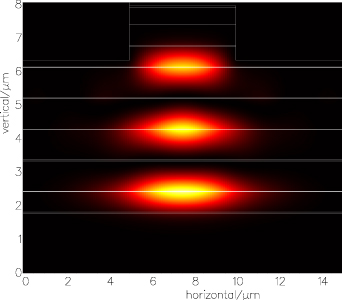
Figure 1. Simulated intensity distribution of the lasing mode in the transverse plane for shallow TJ device with a ridge width of 5 µm. High intensity is coloured bright, low intensity dark. The straight white lines denote boundaries between areas of different refractive indices.
Download figure:
Standard image High-resolution image
Figure 2. Same as figure 1, but for deep TJ device.
Download figure:
Standard image High-resolution imageThe mode distributions of deep and shallow TJ devices correspond to the third vertical mode and fundamental lateral mode having three intensity peaks along the vertical direction at the positions of the QWs and one intensity peak in the region of the ridge laterally. The mode distribution of the shallow TJ device becomes broader with increasing distance from the ridge due to decreasing lateral waveguiding. The mode distribution of the shallow-etched RW laser with a conventional vertical structure utilizing one SQW and no TJs (denoted as 'shallow reference') shown in figure 3 exhibits a single peak both vertically and laterally at the position of the QW below the ridge.
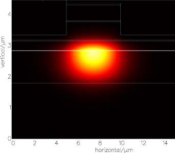
Figure 3. Same as figure 1, but for shallow reference device.
Download figure:
Standard image High-resolution image3. Device fabrication
Two wafers, originating from different metal–organic vapour phase epitaxy runs but having the same vertical structure, are used for the fabrication of the shallow and deep TJ lasers. A third wafer with the conventional vertical structure was grown to fabricate the reference lasers.
To fabricate the RW lasers, a 1.1 μm thick photoresist mask exposed with an I-line wafer stepper was used to pattern the ridges with widths between 3 μm and 100 μm in pairs of 20 μm wide trenches. A chlorine-containing reactive ion etching (RIE) plasma was used to etch the trenches to the calculated target etch depth, stopping before etching through the first or third QW layers, as shown in figure 3. The RIE etching itself was monitored by in-situ interferometry to achieve the optimum etch depth. After insulator deposition (SiNx ) and contact window opening via RIE, a p-metallization layer stack, consisting of Ti/Pt/Au is deposited. After wafer thinning and n-side metallization, consisting of Ni/Ge/Au/Ti/Pt/Au, was sputtered and laser bars are cleaved. Figures 4 and 5 show scanning electron microscope (SEM) pictures of fabricated shallow and deep TJs devices.

Figure 4. SEM picture of the transverse cross section of the shallow TJ structure.
Download figure:
Standard image High-resolution image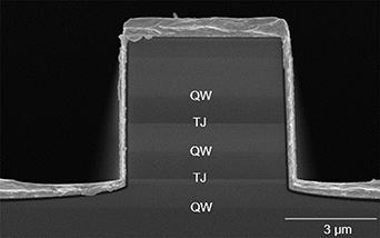
Figure 5. SEM picture of the transverse cross section of the deep TJ structure.
Download figure:
Standard image High-resolution image4. Experimental characterization
The experimental characterization was carried out using uncoated and unmounted laser bars attached to a temperature-controlled stage. Each bar comprises all investigated RW lasers with ridge widths from 3 µm to 100 µm and a cavity length of 3000 µm. The devices were measured in pulsed mode with 1 µs long pulses and a repetition frequency of 1 kHz at room temperature. The emission wavelengths of the lasers vary between 898 and 906 nm, depending on structure and ridge width.
The power–voltage–current characteristics for selected ridge widths W of 5, 15 and 100 µm are shown in figure 6 for illustration. The power characteristics above threshold are almost linear for all devices within the current range investigated. It is important to note that all shallow and deep TJ devices achieve a higher slope than the shallow reference devices. For W = 5 µm, the reference device has the lowest threshold current Ith = 35 mA, whereas for W = 100 µm the deep TJ device has the lowest Ith = 360 mA and both shallow-etched devices have similar threshold currents of Ith = ∼400 mA. The higher voltage of the TJ devices can be attributed to the additional active regions (offset two times the photon energy of 1.4 eV) and the additional series resistance due to the thicker epitaxial layer structure and the additional TJs (higher slope of the voltage–current characteristics).
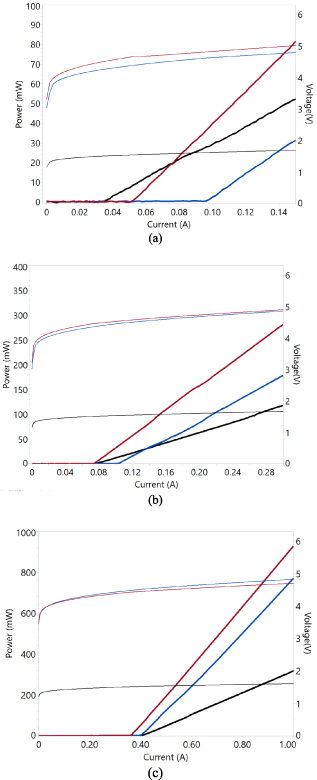
Figure 6. Output power per facet (left axis, thick lines) and applied bias (right axis, thin lines) versus injection current of shallow TJ (blue line), deep TJ (red) and shallow reference (black) lasers with ridge widths of (a) 5 µm, (b) 15 µm and (c) 100 µm.
Download figure:
Standard image High-resolution imageFigure 7 shows the threshold current Ith and external differential efficiency ηdiff in dependence on the ridge widths W. For larger ridge widths (figure 7(a)) the threshold currents exhibit an almost linear dependence on W, indicating a constant threshold current density. The threshold currents of the shallow-etched devices approach each other, whereas the deep TJ has the lowest Ith due to the lack of lateral current spreading (see below). Due to the three active regions, the efficiency of the TJ devices is much larger than that of the reference device. The efficiency of the shallow TJ device (ηdiff = 1.8) is smaller than the efficiency of the deep TJ device (ηdiff = 2.15) due to residual lateral current spreading as discussed below. The external differential efficiency of the deep TJ device is almost three times larger than that of the reference device (ηdiff = 0.75), as expected. The corresponding total slopes of the power–current characteristics are about 3 W A−1 and 1 W A−1, respectively. With decreasing ridge width, the efficiency of the TJ devices strongly declines.

Figure 7. Threshold current (red asterisks, left axis) and external differential efficiency (blue bullets, right axis) versus ridge width. The lines serve as guides to the eye and to distinguish the different structures. Dashed line: shallow reference, dotted: shallow TJ, solid: deep TJ. (a) All ridge widths between 3 and 200 µm. (b) Only small ridge widths.
Download figure:
Standard image High-resolution imageFor small ridge widths (figure 7(b)) the shallow TJ structure results in a deteriorated device performance with enhanced threshold currents and significantly reduced efficiency. The shallow TJ laser with W = 3 µm does not lase at all. We believe that the current spreading and carrier diffusion in the laterally extended TJs, confinement layers and QWs lead to a poor overlap of the lateral mode and carrier density profiles, so that part of the injected electron–hole pairs are not subject to stimulated recombination but do recombine non-radiatively or spontaneously instead. As the width of the ridge increases, this effect becomes vanishingly small so that the shallow TJ devices do lase as well, caused by the decreasing lateral current leakage. The slopes of the deep TJ lasers decline with decreasing ridge widths, too, and their threshold currents are higher than those of the shallow reference lasers. The root cause of this behaviour could be non-radiative recombination at the surfaces of the ridges etched through two active regions (which could deteriorate the lifetime of the lasers, too) as well as additional optical losses due to surface roughness. Nevertheless, the external differential efficiency of the deep TJ laser with a ridge width of W = 6 µm is as high as ηdiff = 1.7, corresponding to a total slope of the power–current characteristics of 2.4 W A−1.
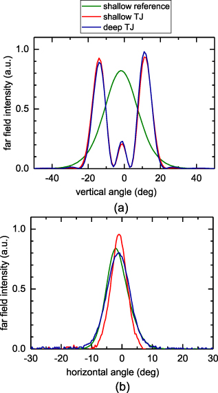
The vertical far field profiles shown in figure 8(a) reveal the lasing of the fundamental vertical mode of the shallow reference device and of the third modes of the TJ devices. The profiles of the deep and shallow TJ devices are almost identical. The lateral far-field profiles shown in figure 8(b) reveal the lasing of the fundamental lateral mode for all lasers. The shallow TJ device exhibits the narrowest lateral divergence due to the weaker lateral optical confinement. The lateral far field angles (full width a half maximum, (FWHM)) for lasers with different ridge width are compiled in table 1. As expected, the lateral far field of the shallow TJ is narrower as the deep TJ device due to the broader near field as revealed by the simulation results (compare figures 1 and 2). For the same reason the far field angle declines with increasing ridge width.
Figure 8. Profiles of vertical (a) and lateral (b) far-field intensity for shallow reference (green line), shallow TJ (red) and deep TJ (blue) lasers having a ridge width of 5 µm measured at an injection current of 150 mA.
Download figure:
Standard image High-resolution image
Table 1. Lateral FWHM angle for different ridge widths.
| Angle (°) | |||
|---|---|---|---|
| Width (µm) | Shallow reference | Shallow TJ | Deep TJ |
| 3 | 8.7 | 6.6 | 10.8 |
| 4 | 8.2 | 6.6 | 8.7 |
| 5 | 8.1 | 6.3 | 8.9 |
| 6 | 6.7 | 4.5 | 8.0 |
5. Conclusions
It was shown in this paper that a structure composed of vertically stacked quantum wells and TJs in a single waveguide core is also suitable for the fabrication of narrow-RW lasers, as long as the strong current spreading due to the TJs can be suppressed, e.g. by etching deep trenches. But even shallow etched RW lasers with three SQWs as active regions exceed single-active-region lasers regarding the slope efficiency. The combination of a vertical structure with multiple active regions and a narrow RW has advantages especially for applications, where low currents, high output power and reasonable beam quality are required, as for example in point-scanning time-of flight LIDAR systems.
Acknowledgments
We are indebted to A Renkewitz for the RIE etching and O Bauer for performing the device measurements.
Data availability statement
The data that support the findings of this study are available upon reasonable request from the authors.
Funding
This work was supported by the Research Fab Germany under Ref. 16FMDQ2 and the German Federal Ministry of Education and Research (BMBF) Grant 13N15566 as part of WiVoPro.
Conflict of interest
The authors have no conflicts to disclose.