
Abstract
We describe the fabrication process and properties of an InP based quantum dot (QD) laser structure grown on a 5° off-cut silicon substrate. Several layers of QD-based dislocation filters embedded in GaAs and InP were used to minimize the defect density in the QD active region which comprised eight emitting dot layers. The structure was analyzed using high resolution transmission electron microscopy, atomic force microscopy and photoluminescence. The epitaxial stack was used to fabricate optical amplifiers which exhibit electroluminescence spectra that are typical of conventional InAs QD amplifiers grown on InP substrates. The amplifiers avail up to 20 dB of optical gain, which is equivalent to a modal gain of 46 cm−1.
Export citation and abstract BibTeX RIS

Original content from this work may be used under the terms of the Creative Commons Attribution 4.0 license. Any further distribution of this work must maintain attribution to the author(s) and the title of the work, journal citation and DOI.
1. Introduction
The emergence of silicon photonics technologies holds the potential of becoming one of the most important revolutions in the field of photonics. The ability to employ highly developed CMOS fabrication for photonic components opens the way for an endless number of transformational applications. The largest hurdle toward this optimistic future is the need to include, within the silicon-based photonic circuits, III–V emitting devices. Several technologies are presently used for this III–V-silicon integration, the most common ones rely on various types of bonding. Heterogeneous epitaxy in which the III–V material is grown directly on silicon is naturally a much better solution but poses difficult problems. Advances have been made for GaAs based devices grown on silicon [1] and the InP based heteroepitaxy technology is progressing as well. InP based integrated photonics enables operation in the telecom wavelength range which is compatible with fiber optics systems and where silicon losses are small.
In order to understand the difficulties in heteroepitaxy, we note that GaAs (1 0 0) consists of two alternating monoatomic layers of Ga and As, and is thus a polar material, in contrast to the nonpolar nature of Si. The growth of GaAs on a Si (1 0 0) surface in a single step can thus lead to the formation of a specific type of defects, the so-called antiphase boundaries (APBs) domain [2, 3]. This problem can be overcome by growing on a double stepped surface. A common way to achieve this, is using a sufficiently tilted Si (1 0 0) surface [3, 4]. An additional problem of GaAs heteroepitaxy on Si is the relatively large lattice mismatch of 4%, which unavoidably leads to the formation of defects in the form of misfit dislocations. The misfit dislocations start bending at each end forming threading dislocations, which propagate relative to the crystal plane at an angle of 60° upwards in the growth direction [2, 5, 6]. These crystal defects lead to non-radiative recombination centers in the optically active layers, which has direct consequences on the device performance. Therefore, it is imperative to reduce the number of dislocations propagating from the Si–GaAs interface to the active layers [7].
Several heteroepitaxy methods have been proposed in the past. One is growing several μm thick relaxation layers which reduce the number of threading dislocations by the annihilation of two such opposing dislocations. However, GaAs layers with a thickness of more than 4 µm exhibit massive cracking, caused by the large mismatch in the thermal expansion coefficient of ca. 60% between GaAs and Si [7, 8]. Another technique to reduce threading dislocations is by introducing strain fields which can bend the dislocations in directions perpendicular to the growth direction [7]. However, a sufficiently large strain initiates additional dislocations. A rather successful technique to combat dislocations is the introduction of strained layer superlattices (SLS), consisting of several periods of thin layers of a strained material (e.g. Inx Ga1−x As and GaAs [9]). Strain fields can also be introduced using quantum dots (QDs) [10]. In either case, Peach–Koehler forces [11] are exerted from the highly strained layers upon the dislocations so that their propagation direction is bent. Hence, they are redirected laterally to the dislocation filter layers (DFLs) and do not reach the optically active regions, which are located close to the top of the structure [7].
The main efforts in realizing III–V QD lasers on Si were focused on 1.3 µm band and devices with excellent properties such as low threshold currents, high operation temperature, and long lifetime were demonstrated [1, 12–15]. However, this turns to be more challenging for devices operating in 1.55 µm band, due to a larger lattice mismatch of 8% between InP-based materials and Si.
Different types of InP-on-Si templates were implemented over the last few years. These include V-groove patterns as well as SLSs or QDs based filter structures. This led to demonstrations of optically pumped CW QD microdisk lasers operating at 4.5 K [16] and also electrically pumped QD microring lasers operating in pulsed mode and in room temperature [17, 18]. Further progress led to room temperature electrically pumped CW operation of quantum dash devices including a QDash microdisk laser on Si [19–21].
However, those structures still suffer from a high defects density, resulting in high operating currents needed to overcome the high internal losses and the low material gain of QDash active material [22].
During the past few years, there has been significant progress in improving the homogeneity of QD ensembles in the InP-based material system operating at 1.55 µm [23]. It resulted in the consequent reduction of the inhomogeneous PL linewidth and a very high spectral material gain. This enabled a record modal gain [24], temperature-stable high-speed lasers [25] as well as wide bandwidth semiconductor optical amplifiers [26] or widely tunable DFB lasers with strongly reduced intrinsic linewidth [27, 28].
This paper describes the fabrication and characterization of high-quality, InP-based QD laser material, monolithically grown on silicon and emitting at telecom wavelengths. InAs QDs are used as the emitting material as well as for the dislocation filtering layers. Due to the large lattice mismatch between InP and Si, a so-called multiple-step strain relaxation technique was implemented [29], which is based on a combination of GaAs and InP based relaxation structures. Namely, the mismatch was compensated gradually by growing GaAs layers between the InP and Si sections.
This results in a complex structure that exhibits a vastly reduced dislocation density at the optically active region. The thick epitaxial stack was investigated by site-specific high resolution transmission electron microscopy (HRTEM) which allowed to map the dislocations as they propagate upwards from the silicon substrate. Optical amplifiers were fabricated and used for the characterization of the optical device quality of the material. The misorientation of the substrate prevented efficient coupling in and out of the amplifier. Nevertheless, the 1 mm long amplifier exhibited an electroluminescence spectrum which resembles that of conventional amplifiers grown on InP substrates and an optical device gain of up to 20 dB, which equals a modal gain of 46 cm−1.
2. Experimental details
The structures were grown by a Varian Gen II solid-source MBE system on three-inch, n-type Silicon (100) wafers, oriented by 5° towards the <110> direction. The MBE system is equipped with valved cracker cells for arsenic and phosphorous. It is well known that this substrate misorientation angle leads to an almost complete double-stepped surface that avoids the formation of APBs [4–6]. Before loading into the growth chamber, the substrates were pre-treated ex-situ with 2.5% hydrofluoric acid (HF) in order to remove the native oxide layer, and subsequently rinsed in purified water. The successful removal is visible as a hydrophobic modification of the surface. The samples were then loaded fastly into the load-lock chamber to minimize surface contamination. The substrate temperature during growth was measured by a pyrometer. Before the growth, the wafer was heated to a minimum temperature of 870 °C for 20 min without As overpressure to remove any residual oxide layer. The As valve was opened while cooling down the substrate from 870 °C to 700 °C in order to reach an As flux of around 5 × 10⁻⁶ Torr beam equivalent pressure (BEP). The As desorption from the Si surface is reduced significantly below 700 °C. The sample was then cooled to 450 °C in order to stabilize the substrate temperature.
The material quality of the structure was characterized by various analytical techniques including x-ray diffraction (XRD), atomic force microscope (AFM), low-temperature photoluminescence (PL) and cross-sectional HRTEM imaging. The grown structures were also processed to SOAs.
The active layer comprised eight layers of InAs QDs, each with a nominal thickness of 4.7 monolayers (MLs). Its PL spectrum was compared with that of a reference laser structure grown on an InP substrate. The top contact and cladding layers were removed in order to enable the PL characterization. The laser structure grown on Si underwent an annealing process by which the sample was heated to 740 °C for 30 s followed by a sudden cooling to room temperature. The annealing process improved the shape of the active QDs making them more pyramidal or dome-like and improving the PL intensity while blue shifting the peak intensity. The material composition and the strain values between the different buffer layers were examined by XRD.
The HRTEM characterization made use of a monochromatic and double corrected S/TEM Titan Themis Thermo-Fisher, used in both TEM and STEM modes. A Bruker Dual-X EDS detector was used for acquiring elemental maps. Cross section samples for the HRTEM characterization were prepared by an FEI Helios Nano lab Dual Beam G3 UC Focused Ion Beam system. The thick epitaxial stack was divided into two parts in order to prepare high quality TEM samples.
Since the laser cannot be contacted from the substrate side, a special design and fabrication process where both contacts are placed on top of the structure was developed. A schematic description of the device is shown in figure 1(a) while figure 1(b) shows a scanning electron microscope cross-section of the device. Figure 1(b) shows neither the n contact nor the detailed epitaxial layer structure.
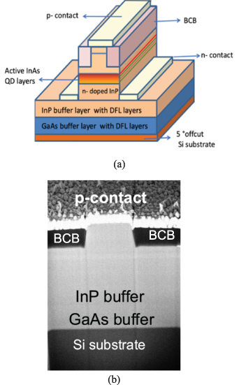
Figure 1. (a) Schematics of the device with two top contacts. (b) SEM cross-section of the device.
Download figure:
Standard image High-resolution imageThe ridge waveguides were structured by optical contact mask lithography and dry chemical etching with chlorine and argon-based plasma. A silicon dioxide hard mask, fabricated by lift-off was used since it offers a better etch selectivity than an optical resist. Two trenches were etched, using the same plasma etch recipe, on both sides of the ridge, down to the thick highly doped n type InP layer. The trenches were situated symmetrically with a separation of a few μm in order to enable efficient lateral current injection. The n contacts consist of a nickel–germanium–gold stack that was alloyed using rapid thermal annealing at 390 °C. The entire chip was planarized with benzocyclobutene (BCB). Since the ridges were covered after spin-coating of the polymer, it was necessary to etch back to the ridge surface by dry etching with CHF3 and O2. The p contact was formed by lift-off after deposition of titanium, platinum and gold. Since the n contacts were covered with BCB, windows had to be opened by dry etching in order to contact them prior to metallization. Finally, the laser chip was thinned to about 110 µm by polishing with an Al2O3 slurry to facilitate cleaving of the SOA facets. Due to the crystal misorientation, the facets were angled what complicated the fiber coupling.
3. Results and discussion
3.1. Direct epitaxial growth of InP based III-V QDs material on silicon
QDs based DFL in GaAs and InP were optimized separately and some of them were studied using HR-TEM in order to map the dislocation blocking efficiency. The optimum GaAs and InP based relaxation buffers were later combined so that the complete laser structure could be grown monolithically on a Si wafer.
3.1.1. Optimization of GaAs-based DFL.
For the initial GaAs buffer layer on Si, the so-called two-step growth method was used [30, 31], where a 36 nm thick GaAs grown at 350 °C, with a low nominal V/III ratio of 15 (based on the BEP values) and a growth rate of 200 nm h−1 served as a nucleation layer. Accurate control and optimization of the low-temperature GaAs nucleation layer results in a noticeable reduction of the defect density in the overall GaAs epilayer. InAs QDs were selected to serve as the dislocation filter for the defects originating at the Si/GaAs interface due to their much larger dislocation bending area ratio [7, 32] compared to other types of dots, e.g. InGaAs QDs. A few test samples incorporating InAs QD layers with a nominal thickness of 1.42–3.47 ML, grown at 490 °C on top of a 100 nm GaAs buffer layer which was deposited in turn after the GaAs nucleation layer on the Si wafer were fabricated. AFM measurements were used to assess their suitability as QD based DFL. The 3.47 ML thick sample yielded rather large dots with lateral dimensions of 80–130 nm at a QD density of 1.9 × 1010 cm−2. The QD height was 16–21 nm. Very large dots generate new dislocations [7, 33, 34] and are therefore unsuitable for QD based defect filters. The QDs nominal thickness of 1.89 ML results in a QD density of 1.6 × 1010 cm−2 with lateral sizes and heights in the range of 40–60 nm and 5–8 nm, respectively. These types of QDs were chosen as filter layers. A series of samples incorporating 2, 3, 5 and 10 QD filtering layers and with varying growth conditions of 100 nm thick GaAs spacer between the InAs filtering dot layers were grown on Si and characterized with low-temperature PL. Optically active buried In0.5Ga0.5As QDs, grown at 450 °C, were placed above the filter structures in order to test the reduction of threading dislocations using PL measurements [7, 31, 35–37].
Samples showing high PL intensities were investigated by HRTEM.
The number of filtering layers, the temperature cycling and interruptions of the deposition during the growth of the QD filter structures and the GaAs spacers were found to have a profound effect on the effectiveness of dislocation blocking. The best results were achieved for conditions where the QDs filter layers, as well as GaAs spacers, were deposited at a constant temperature of 490 °C without any interruptions. Our findings differ somewhat from some previous studies where the high-growth-temperature GaAs spacer layer was assumed to inhibit the formation of additional threading dislocations [7], thereby improving characteristics of 1.3 µm dot-in-a-well lasers grown on GaAs, though the mechanism by which the dislocation formation was suppressed remained unclear [38, 39]. In another work [31] authors claimed the improvement in PL intensity of active QDs due to in situ annealing of the InGaAs/GaAs SLS-based DFL during the high-temperature growth of GaAs spacer layers at 610 °C increasing the dislocation motion, which aided mutual dislocation elimination. The authors do not refer to the formation of new dislocations within the GaAs spacer during the temperature ramping from 420 °C to 610 °C. Nevertheless, both cases cannot be compared with the results presented here due to the differences in substrates, structure design and type of the DFLs used.
Figure 2 shows the impact of the GaAs-based DFL structures on Si that consists of one and two stacks of five filtering QD layers, on the PL spectra measured at 10 K and emitted by the active InGaAs QDs grown above them. For comparison, the PL spectra of the reference samples grown directly on GaAs as well as one gown on Si wafer but without any DFL structure are included. All four samples were grown in a manner that the total thickness of the GaAs-buffer grown before the active dots (with or without DFL) was fixed at1600 nm. The reference sample without any DFL (dashed line) showed a weak PL signal, whose integrated intensity was only 36% of the reference InGaAs QDs grown on GaAs (solid line). The PL intensity was improved significantly by the DFL reaching integrated intensities of 59% and 84% of the GaAs reference sample for the single and double stack filtering layers, respectively.
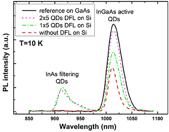
Figure 2. Low-temperature PL spectra of the reference samples with the active InGaAs QDs grown directly on GaAs (solid black line) and Si wafers (dashed red line) without any DFL compared to the samples implementing one (dash-dot green line) and two periods (dotted magenta line) of five InAs QDs filtering layer each. The PL peak around 920 nm originates from the DFL themselves. The spectra were recorded at 10 K with an excitation power density of 10 W cm−2.
Download figure:
Standard image High-resolution imageIn addition to the PL signal from the active InGaAs QDs, figure 2 also shows a PL signal near 920 nm originating from the filtering dots. The 920 nm peak position is much shorter compared to the InAs filtering QDs in [7], emitting around 1350 nm at room temperature. This testifies to the very large difference in filtering dot size, even taking into account the bandgap shrinkage at 300 K. The authors in [7] observed an enhanced PL intensity from the active dots in structures implementing large filtering QDs. However, those PL peak intensities were two times lower compared to the reference structure grown on a GaAs wafer. This is another important difference, confirming that smaller filtering dots developed here, are more suitable for defect filtering in GaAs/Si structures.
3.1.2. Growth of the full InP-based laser structure on Si.
The laser structure growth was split into three steps. Initially, the GaAs dislocation filter, shown in figure 3(a) was grown. The growth was continued with an InP on GaAs relaxation filter as seen in figure 3(b), and finally, the entire InP-based laser structure, including the emitting QD layer was grown as shown in figure 3(c).
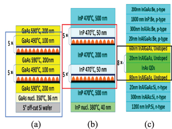
Figure 3. Schematics of the three parts forming the full laser structure monolithically grown on Si: (a) GaAs based dislocation filter; (b) InP based dislocation filter; (c) laser structure layer design. The series of nominally 1.89 ML and 5 ML thick InAs QDs layers serve as the dislocation filters in GaAs and InP buffer structures, respectively.
Download figure:
Standard image High-resolution imageThe GaAs-based DFL was formed by two periods of five highly strained InAs QDs layers separated by 100 nm of GaAs, both grown at 490 °С, as described in the previous section. The 200 nm thick GaAs layer between the two filter stacks as well as the layer above the filter structure were grown with a V/III ratio of 20 and a growth rate of 800 nm h−1 at 590 °C, to smoothen the growth front. The entire structure creates a kind of a virtual GaAs substrate for further growth of the InP dislocation buffer, presented in figure 3(b).
Similar to the GaAs buffer, the InP growth starts with a 40 nm thick nucleation layer grown at a low temperature of 380 °C and a relatively low rate of 250 nm h−1. The rest of the InP buffer was grown at 470 °C with an InP/InAs growth rate of 450 nm h−1. Although the lattice constant difference between InP and GaAs is moderate, the heterointerface is nevertheless another source of a large number of defects. Therefore, an additional filtering structure was used in the InP buffer above the nucleation layer. For this purpose, two stacks of nominally 5 ML thick InAs QDs deposited on a 2 nm InP-lattice-matched InAlGaAs layer and capped by 50 nm of InP were used. Each stack consists of five periods and is separated by a 200 nm InP layer. An additional 500 nm InP layer was grown following the second filter stack.
An InAlGaAs wetting layer was used in order to initiate the nucleation of high density, limited sized dots. Unlike in [36], we did not apply a strained wetting layer, and the growth without As overpressure was not interrupted after the filter dots were grown. Nevertheless, an RMS value of 3.7 nm was obtained evaluated from a 2.5 × 2.5 µm2 AFM scan made on the top of the 500 nm InP layer just before the laser structure growth.
The filter structures served as the basis for the growth of a laser structure as shown in figure 3(c). The laser structure comprised a stack of eight self-assembled InAs QDs active layers separated by 20 nm thick In0.528Al0.238Ga0.234As barriers. The active region was embedded in a 100 nm thick quaternary waveguide layer of the same composition as the barriers separating the QD layers. Each QD layer was formed by deposition of 4.5 MLs InAs at 490 °C in an As2 environment using an InAs growth rate of 450 nm h−1. The lower cladding layer (n side) consists of a 1200 nm thick InP buffer and a 300 nm In0.523Al0.477As layer. On the p side, the upper cladding was formed by 300 nm In0.523Al0.477As and 1800 nm InP followed by a 200 nm thick highly p doped In0.532Ga0.468As contact layer. The n and p side layers were doped by Si and Be, respectively. All materials, except the InAs QDs, are nominally lattice matched to InP. The bottom thick n-type InP layer is accessed from the top for the lateral current injection and enables a low resistance.
The laser top surface morphology was characterized by AFM. An image of a 10 × 10 μm2 AFM scan with a low surface roughness of 4.8 nm RMS, similar to the best reported value for InP integrated on Si [29], is shown in figure 4. Scanning a smaller area of 1 × 1 μm2, yielded an RMS roughness of only 1.9 nm. A few pinholes which might be caused by the penetrating defects are seen in the AFM image. The estimated defect density was below 107 cm−2. This density is sufficiently low for not having a large impact on the basic structure performance.

Figure 4. Surface morphology of the laser structure grown on Si characterized by AFM. For a 10 × 10 µm2 and 1 × 1 µm2 scan, the RMS roughness of 4.8 nm and 1.9 nm were found, respectively. The estimated density of the observed pinholes is below 107 cm−2.
Download figure:
Standard image High-resolution imageThe role of the dislocation filters was characterized using HRTEM by following the evolution of the dislocations as they propagate from the first interface with the silicon substrate towards the active region where the emitting QDs are placed. The dislocation distribution is described in figure 5 where each image corresponds to a region as indicated by squares in figure 3.
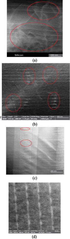
Figure 5. HRTEM images (a) Si–GaAs interface corresponding to the blue square in figure 3(a). (b) InP dislocation filter corresponding to the red square in figure 3(b). (c) Emitting QDs corresponding to the black square in figure 3(c). Figure (c) shows also thick lines placed below the emitting QDs which originate from the FIB sample preparation. (d) High magnification image of the active InAs QD layers. The scale bar length corresponds to 200 nm in images (a)–(c) and 10 nm in (d).
Download figure:
Standard image High-resolution imageThe largest defect density is naturally seen near the silicon interface, figure 5(a). The region where the image was taken is indicated by a blue square in figure 3(a). The dislocation density reduces significantly in the vicinity of the InP part. This corresponds to the red square in figure 3(b). The image is shown in figure 5(b). Finally, in the region of the eight layers emitting QDs, indicated by a black square in figure 3(c), the dislocations are all but diminished as shown in figures 5(c) and (d). The eight QD layers are depicted in figure 5(c) while a higher resolution image where individual dots are clearly seen, is shown in figure 5(d). Figure 5(c) shows also thick lines placed below the QDs. These are artefacts originating from the Ga beam during the FIB preparation and are not to be mistaken for defects stemming from the epitaxial growth.
In order to further investigate the quality of the dislocation filters, we repeated the HRTEM examination of the emitting QDs, this time imaging several areas within the cross-section. This enables a more reliable conclusion as to the defect density where it is most crucial. Figure 6 shows four such images, all of which show only very few defects. A rough estimate of the defect density in the vicinity of the emitting QDs is 108 cm−2 which is low enough to allow high optical gain but may be too large for reliable operation over a long time.
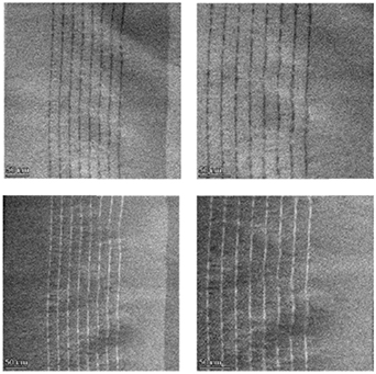
Figure 6. Four HRTEM images at different locations within the cross-section in the vicinity of the emitting QDs show only very few defects. A rough estimate of the defect density is 108 cm−2. The scale bar length corresponds to 50 nm in every image.
Download figure:
Standard image High-resolution imageFigure 7 compares low-temperature PL spectra of the full laser structure grown monolithically on Si with a reference laser structure of a similar design grown on an InP substrate. The laser structure grown on Si exhibits quite an intense PL emission with a Gaussian spectral shape. The peak intensity is reduced by 20% in comparison to the reference sample. However, the PL linewidth is 56 meV (FWHM) which is broader than the linewidth of the reference laser of 35 meV. Therefore, the integrated PL intensities are comparable confirming the high quality of the QDs grown on silicon. It is difficult to compare the obtained FWHM for the laser on Si with literature data since most reports present room temperature PL spectra, which are quite broad, have asymmetric shape and show three to four times lower PL peak intensity compared to the reference samples grown on InP [18, 19, 21]. In one work [16], the PL spectra of a microdisk laser, measured at 4.5 K showed a FWHM of about 100 meV, which is almost two times broader compared to our result.
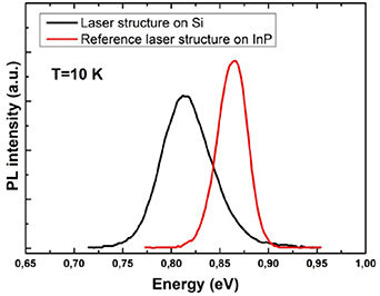
Figure 7. Comparison of low-temperature PL spectra for the laser structure monolithically grown on Si and a reference laser structure having a similar design but grown directly on an InP substrate. The PL peak position corresponds to 1520 nm and 1433 nm for Si- and InP-based structures, respectively. The spectra were recorded at 10 K with an excitation power density of 10 W cm−2.
Download figure:
Standard image High-resolution image3.2. Optical gain
The entire laser structure was used to fabricate 1 mm long optical amplifiers with a ridge width of 2 µm. Cleaving the structure grown on the misoriented substrate resulted in a 18°–20° output emission angle relative to the ridge axis as well as to the substrate. This prevented efficient coupling in and out of the amplifier. Nevertheless, it is possible to measure accurately the chip gain which is an important measure of the epitaxy quality.
Figure 8 presents bias dependent electroluminescence spectra whose bandwidth and character are essentially the same as that of spectra measured for nominally identical amplifiers grown on InP substrates.
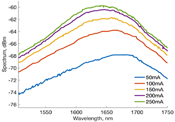
Figure 8. Bias dependent electroluminescence spectra of the QD SOA grown on silicon.
Download figure:
Standard image High-resolution imageFigure 9 shows measured bias and input power dependent chip gain. The large input coupling losses prevented gain saturation however, it is easy to extract the small signal chip gain which reached 20 dB. The corresponding gain coefficient is 46 cm−1 at a current density of 1.4 kA cm−2 which is consistent with the modal gain of high quality QD lasers grown on InP. The large gain values testify the high-quality gain region of the optimized structure. Moreover, this gain value is 53% larger than the recently reported value for the InAs QDash laser grown on a patterned (with V-shaped nano grooves) Si substrate utilizing InGaAs/InP SLS based DFL [22].

Figure 9. Bias and input power dependence of the chip gain.
Download figure:
Standard image High-resolution image
4. Conclusions
To conclude, we have described the fabrication process and the structural and optical properties of InAs QDs grown on an off-cut silicon substrate and emitting at telecom wavelengths. The epitaxial system includes several layers of QD based dislocation filters embedded in both GaAs and InP. These dislocation filters ensure that the large defect density near the silicon interface is all but diminished at the emitting QD region. Optical amplifiers made with this epitaxial material exhibit up to 20 dB gain corresponding to a modal gain of 46 cm−1 as well as a bias dependent electroluminescence spectrum which is comparable to that of similar QDs grown on an InP substrate.
Acknowledgments
This research was funded through European Union Horizon 2020 research and innovation programme under Grant Agreement No. 780537, project MOICANA (Monolithic cointegration of QD-based InP on SiN as a versatile platform for the demonstration of high performance and low cost PIC transmitters), www.moicana.eu.
Data availability statement
All data that support the findings of this study are included within the article (and any supplementary files).