
Abstract
Memristive and resistive switching devices are considered promising building blocks for the realization of artificial neural networks and neuromorphic systems. Besides conventional top-down memristive devices based on thin films, resistive switching devices based on nanowires (NWs) have attracted great attention, not only for the possibility of going beyond current scaling limitations of the top-down approach, but also as model systems for the localization and investigation of the physical mechanism of switching. This work reports on the fabrication of memristive devices based on ZnO NWs, from NW synthesis to single NW-based memristive cell fabrication and characterization. The bottom-up synthesis of ZnO NWs was performed by low-pressure chemical vapor deposition according to a self-seeding vapor-solid (VS) mechanism on a Pt substrate over large scale (∼cm2), without the requirement of previous seed deposition. The grown ZnO NWs are single crystalline with wurtzite crystal structure and are vertically aligned respect to the growth substrate. Single NWs were then contacted by means of asymmetric contacts, with an electrochemically active and an electrochemically inert electrode, to form NW-based electrochemical metallization memory cells that show reproducible resistive switching behaviour and neuromorphic functionalities including short-term synaptic plasticity and paired pulse facilitation. Besides representing building blocks for NW-based memristive and neuromorphic systems, these single crystalline devices can be exploited as model systems to study physicochemical processing underlaying memristive functionalities thanks to the high localization of switching events on the ZnO crystalline surface.
Export citation and abstract BibTeX RIS

Original content from this work may be used under the terms of the Creative Commons Attribution 4.0 license. Any further distribution of this work must maintain attribution to the author(s) and the title of the work, journal citation and DOI.
1. Introduction
The ever growing advances of information processing has pushed the development of metal-oxide-semiconductor field-effect transistors driven by Moore's law [1] and Dennard scaling [2]. However, cost-effective scaling of this technology is nowadays hampered by physical limitations encountered by further shrinking technology nodes. Also, the traditional von Neumann computing architecture is challenged by the development of an ever growing interest in data-centric computing and machine learning in the era of Big Data and internet of things. Indeed, performances of this architecture are limited by the so-called von Neumann bottleneck related to the continuous data transfer in between the central processing unit and the memory. In this framework, memristive devices are considered as promising building blocks in the semiconductor industry for the development of new computing approaches and architectures [3]. In these two-terminal devices, where ionics is coupled with electronics, functionalities rely on the so-called resistive switching mechanism responsible for the dependence of the internal state of resistance on the history of applied voltage and current [4]. For this reason, memristive devices have been proposed for a wide range of applications including next generation memories, in-memory computing, brain-inspired computing and neuromorphic systems for the emulation of biological synapses and neurons [5–7].
Conventional memristive devices are realized through a top-down approach where an active material (typically a metal oxide thin film) is sandwiched in between two metal electrodes in a metal–insulator–metal (MIM) structure [8]. Representing an ideal approach for reducing the device size beyond the limits of top-down lithography, memristive devices based on nanostructures realized with a bottom-up approach have been investigated [9]. In this framework, resistive switching planar devices based on nanowires (NWs) have been reported as good platforms and model systems for studying and analysing the intrinsic switching mechanism. Indeed, differently from conventional memristive cells based on thin films where switching phenomena are buried in the MIM sandwich structure, the switching mechanism in NWs can be highly localized allowing direct investigation of electrochemical reactions and ionic transport phenomena underlaying memristive behaviour [10–13]. In addition, thanks to the possibility of tuning the electrical transport at the nanoscale and by exploiting surface states, new resistive switching features can be achieved in NW-based memristive devices by light stimulation [14, 15] or by properly engineering surface electronic properties [16, 17].
Among nanostructures, ZnO NWs and nanorods have attracted great interest during last years because of their remarkable physical properties and potential applications in optoelectronics, biomedical sciences, bio and gas sensing, nanogenerators and photocatalysis, where isolated NWs or group of NWs are exploited as active elements [18–20]. In particular, ZnO NWs have been also widely exploited for the realization of NW-based resistive switching devices [9]. A wide range of resistive switching devices based on single ZnO NWs [10, 21–29] and NW arrays [30–33] have been reported, where NWs were synthetized by different growth techniques. Among growth techniques, ZnO nanostructures have been reported to be synthetized by chemical vapor deposition (CVD) with a wide range of setup configurations and process parameters, as well as different growth mechanism such as vapor-liquid-solid (VLS) and vapor-solid (VS) [34–44]. In case of VLS mechanism, small liquid metal clusters have to be formed on the growing substrate to act as catalysts for the incorporation of precursor atoms with consequent growth of nanostructures by precipitation. Instead, no catalyst is required in case of VS growth since in this case nanostructures are crystallized directly on the growing substrate. In this framework, the synthesis mechanism and process parameters have to be optimized depending on the desired material quality and final application.
In this work, the fabrication of memristive devices based on ZnO NWs is reported, from NW synthesis to single NW-based memristive cell fabrication and characterization. In particular, the bottom-up synthesis of ZnO NWs by self-seeding VS mechanism on a Pt substrate was reported, showing that this growth mechanism allows to grow vertically aligned, single crystalline and hexagonal-shaped ZnO NWs with wurtzite crystal structure over large scale (∼cm2), without requiring pre-deposition of a seeding layer. The growth mechanism is discussed by investigating the role of the growth substrate and by analysing the effect of growth parameters on resulting NW dimensions and density. Then, the fabrication process of memristive cells based on single crystalline ZnO NWs asymmetrically contacted by means of an electrochemically active and an electrochemically inert electrode is reported. The single NW-based device, acting as an electrochemical metallization memory (ECM) cell, exhibits reproducible resistive switching behaviour with a relatively high ON/OFF resistance ratio. Furthermore, it is able to emulate features of biological synapses such as paired pulse facilitation (PPF), with gradual increase of device conductance upon stimulation with temporally correlated voltage pulses. These NW-based memristive devices represent versatile building blocks for nanoelectronics towards the realization of NW-based neuromorphic systems.
2. Synthesis of ZnO NWs by CVD
2.1. Experimental CVD setup
The synthesis of ZnO NWs was performed by means of a low-pressure chemical vapor deposition (LPCVD) process in a horizontal tubular furnace, as schematized in figure 1(a). The LPCVD furnace is composed of a flanged quartz tube connected with two gas lines that allow the insertion of precursor and carrier gases. The total gas flux flowing into the process chamber and the ratio in between different gas species is regulated by means of flowmeters. Heating components surrounding the quartz tube allow to heat up the sample during the deposition process. The growth process was performed on a Pt target substrate that was realized by sputtering on a SiO2 commercial wafer substrate. An adhesion layer of Ta was inserted by sputtering prior to Pt deposition to increase the adhesion of the Pt film on the underlying substrate. The Pt growth substrate was placed in the process chamber on an alumina boat, surrounded by a Zn foil (99.99% of purity) that acts as the Zn source during the CVD. In order to obtain reproducible growth conditions, the quartz tube was cleaned from Zn and ZnO residues after each growth process with an HCl solution.

Figure 1. Synthesis of ZnO NWs by low pressure chemical vapor deposition (LPCVD). (a) Schematization of the experimental apparatus for the synthesis of ZnO nanostructures by LPCVD. (b) Low-pressure chemical vapor deposition process for the synthesis of ZnO NWs consisting in a heating step, a CVD step of NW growth and a cooling step. (c) Schematization of the ZnO NWs growth process by CVD, consisting in an initial nucleation of ZnO islands to form a ZnO base and consequent growth of NWs along the preferential c-axis direction. Each growth stage refers to a different step of the growth process of panel (b).
Download figure:
Standard image High-resolution image2.2. ZnO NWs synthesis process and mechanism
Before the LPCVD process, the process chamber was evacuated down to the ∼10−2 Torr to remove contaminations. Then, during the heating step, the Zn source and Pt substrate were heated up with a ramp rate of 8.6 °C min−1 while fluxing 60 sccm of Ar. The flux of Ar, exploited as carrier gas during the synthesis, was increased to the target value desired for the growth process (in the range of 250–400 sccm) when temperature reached 300 °C. When the target temperature of 650 °C was reached, the CVD step started and a flux of O2 exploited as gas precursor was inserted into the chamber in addition to the Ar flux. During this growth stage, the temperature was maintained fixed at 650 °C for 20 min. The growth pressure, that depends on the amount of gases fluxed into the chamber, was measured to be in the range of 1–1.6 Torr. At the end of the CVD step, the O2 flux was interrupted, and the chamber was cooled down to room temperature in a Ar environment. The whole procedure with different phases is reported in figure 1(b).
2.3. Growth mechanism and NW morphology
The ZnO NW growth process during the CVD step can be explained by means of a self-seeding vapor-solid (VS) mechanism, as schematized in figure 1(c). During the heating step, the Zn source melts (the melting point of Zn is about 420 °C in ambient conditions) and, when the vapor tensions of the liquid Zn is high enough, starts to evaporate. Helped by the carrier gas, the Zn is transported on the target Pt substrate. After diffusion of reactant species and absorption on the Pt surface, during the early stage of growth when O2 is inserted into the chamber, ZnO starts to nucleate on the Pt substrate with consequent growth of ZnO islands. Then, while growth of additional islands occurs near the existing ones coalescing into a polycrystalline continuous ZnO base layer, ZnO islands act as seeds for the synthesis of ZnO NWs that grow fed by the evaporated zinc sources and oxygen elements, as similarly reported by Jeong and Lee [45]. The nucleation of seeds is likely to be facilitated in correspondence of Pt grain boundaries and substrate defects [46]. Since the growth of ZnO NWs occurs epitaxially along the c-axis crystallographic direction of the seed, the NW alignment is determined by the crystallographic orientation of islands formed during first stages of the CVD step. An investigation of the NW morphology by SEM imaging after the growth process revealed that the LPCVD process resulted in vertically aligned NWs (figure 2(a)). The NW growth was observed to be uniform over relatively large area (∼2 × 2 cm). Cross-section images reported in figure 2(b) allows direct observation of the ZnO base layer, sandwiched in between NWs and the Pt substrate, formed during initial stages of the growth process. In addition, a high-resolution image (figure 2(c)) revealed the typical hexagonal shape of NWs related to the wurtzite crystal structure with P63mc symmetry resulting from the growth process that proceeds along the [0001] polar direction (c-axis). Detailed structural and chemical characterization of as grown ZnO NWs reported in our previous works [30, 47] revealed that each NW is a single crystal with high chemical purity and a clean surface without the presence of any amorphous layers.

Figure 2. Morphology of ZnO NWs synthetized by LPCVD. (a) Tilted SEM image showing vertically aligned NWs (scale bar, 1 µm). (b) Cross-sectional SEM image of ZnO NWs showing the presence of a ZnO base layer in between vertically aligned NWs and the Pt growth substrate (scale bar, 500 nm). (c) Detail of a NW tip showing the hexagonal shape and the absence of metal clusters on the NW top (scale bar, 30 nm).
Download figure:
Standard image High-resolution image2.4. The role of the substrate
The VS growth mechanism based on self-seeding overcomes issues related to the pre-deposition of a seed layer. In this context, nucleation is strongly related to the properties of the growth substrate and Pt was observed to be an optimal substrate for self-seeding and nucleation of ZnO nanostructures. In order to clarify this aspect, NWs grown on a bare Pt substrate were compared to NWs grown on a pre-seeded substrate. The seed layer was realized by preparing a solution of zinc acetate dihydrate (22 mg) and ethanol (10 ml) on a Pt substrate. This solution was then deposited on a Pt clean substrate by spin coating and subsequent dipping in ethanol. By following this procedure, five seed layers were realized and then baked at 350 °C for 20 min. This procedure was performed 2 times, for a total of ten seed layers. A pre-seeded and bare Pt substrate was then inserted together in the growth chamber and a CVD process was performed by flushing 150 sccm of O2 and 300 sccm of Ar. Results evidenced that NWs with similar morphologies were synthetized in case of pre-seeded and bare Pt substrates, as reported in figures 3(a) and (b), respectively, clearly showing that the seeding procedure can be safely avoided without influencing the resulting NW morphology. Similarly, other metals including Ti, Mo and W were reported as substrates for initiating the growth of ZnO NWs [36]. Interestingly, the here reported growth mechanism allows selective growth of ZnO NWs by pre-patterning the Pt substrate since nucleation is suppressed elsewhere. This can be clearly observed in figure 4 where it can be observed that NWs grows only where Pt was present, while other ZnO nanostructures, such as nanobelts and sponge-like structures, were observed on the bare Si substrate.

Figure 3. The role of the growth substrate. Comparison of ZnO NWs grown on a (a) pre-seeded and (b) bare Pt substrate (scale bars, 500 nm).
Download figure:
Standard image High-resolution image
Figure 4. Selectivity of the growth process. (a) ZnO NWs grows only on the Pt substrate (right side) while on the bare Si substrate other ZnO nanostructures can be identified (scale bar, 2 µm). Cross-sectional images of (b) nanostructures grown on the Si substrate (scale bar, 10 µm) and (c) vertically aligned NWs grown on the Pt substrate (scale bar, 500 nm).
Download figure:
Standard image High-resolution image2.5. NW dimensions and density
Controlling the dimensions during the synthesis represents a crucial aspect for the growth of NWs by means of bottom-up techniques. In order to investigate the effect of growth parameters on NW dimensions, we have evaluated changes in the NW dimensions by varying the precursor gas flux during the process. For this purpose, different LPCVD processes were performed by changing the O2 flux in the range 50–200 sccm by keeping all the other parameters fixed (T = 650 °C, t = 20 min, Ar flux of 300 sccm). The resulting distributions of NW lengths and diameters are reported in figures 5(a) and (b), respectively. Measurements were performed by evaluating SEM cross-sectional images in different areas of the sample, while sample-to-sample and process-to-process variability was taken into account by considering two samples for each set of parameters in two distinct LPCVD growth process. Note that in all cases the hexagonal shape of NWs was preserved. Results show that the NW morphology can be tuned by varying the O2 flux during the synthesis process. In particular, the NW length can be tuned from ∼980 nm in case of 150 sccm of O2 up to ∼1.7 µm in case of 200 sccm of O2. Interestingly, it can be observed that an increase of the precursor gas from 50 to 150 sccm resulted in shortening of NWs. Even if a detailed understanding of this trend still needs further investigation, it can be to strongly different thermodynamic conditions obtained by increasing the O2 flux while maintaining constant the Ar flux, resulting in an increase of the total gas flux. The NW diameter, instead, was observed to be nearly constant at about 80 nm independently from the O2 flux. As a consequence, the aspect ratio exhibited a similar trend respect to the NW length, as reported in figure 5(c), where it can be observed that NWs with aspect ratio from ∼12 up to ∼22 can be obtained. Importantly, it was observed that the ZnO base layer thickness follow the same trend of the NW length as reported in figure 5(d), suggesting that the base layer thickness increases in parallel with the growth of NWs.

Figure 5. ZnO NW dimensions as a function of the O2 flux during the growth process. All processes were performed by keeping constant all the other growth parameters (T = 650 °C, t = 20 min, Ar flux of 300 sccm). Box plots of (a) length, (b) diameter, (c) aspect ratio and (d) base layer thickness. Midlines are median values, squares the mean values, boxes the 25th and 75th percentiles and whiskers the 10th and 90th percentiles. Each distribution was obtained by evaluating two different samples for each growth condition, by evaluating the dimension of at least 200 NWs in different areas of the sample.
Download figure:
Standard image High-resolution image3. Single NW memristive cell fabrication and characterization
3.1. Single NW memristive cell fabrication
Single NW devices with asymmetric electrodes can be realized by means of combined photolithography and electron beam lithography (EBL). In the first step, a commercial insulating substrate of SiO2/Si was patterned by means of photolithography to realize a customized millimetric Au probe circuit. Then, a mounted hair was used to mechanically transfer NWs from the growth substrate to a selected area of the probe circuit (∼120 × 120 µm), helped by an optical microscope. Subsequently, by exploiting markers as references, isolated NWs were selected and then one side was contacted to the probe circuit through EBL patterning with following metal deposition and lift-off technique. Before metal deposition, a plasma treatment (40 W, 30 s) was exploited to enhance contact quality and reliability. Then, a second EBL process was performed to realize the contact electrode on the opposite side. The schematic process flow for the realization of single NW devices with associated SEM images for each step is reported in figure 6. During the whole fabrication process, the exposure of NWs to aqueous solutions was strictly avoided in order to preserve the ZnO NW surface from degradation, as investigated in our previous work [47]. For the realization of a single NW memristive cells, ZnO NWs have been asymmetrically contacted by means of an electrochemically inert and an electrochemically active electrode, as discussed in the following. Note that the channel length of the device (i.e. the distance in between electrodes) is determined during the lithographic processes, while the NW diameter is defined by the growth process. In this framework, it is worth noticing that a possible downscaling of the NW diameter below 10 nm can be achieved by exploiting catalyst-assisted growth techniques with nanoparticles catalyst templates, as for example reported by Yin et al [48]. In addition, note also that this fabrication process flow can be exploited for the realization of memristive devices based on a wide range of metal-oxide NWs and nanostructures.
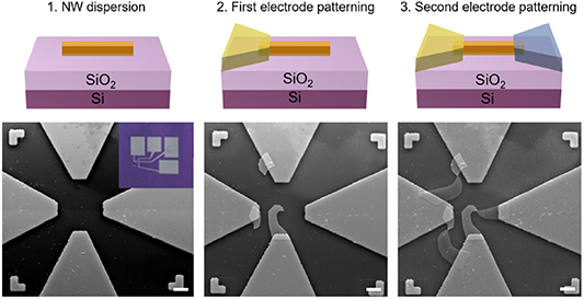
Figure 6. Fabrication of single NW devices. NWs are initially dispersed on a selected region of a pre-patterned probe circuit with millimetric pads realized with photolithography. Then, electron beam lithography (EBL) and subsequent metal deposition were exploited to pattern an electrode contacting one side of the NW with the pre-patterned probe circuit. Similarly, a second electrode with a different metal was realized with a second lithographic step. For each step of fabrication, a SEM image is reported (scale bar, 10 µm). The inset in the left SEM image reports the pre-patterned probe circuit, where pad lines allow to connect the central region (where NWs are dispersed) with millimetric pads for electrical connection of external probes. In all SEM images, markers were used for the alignment of electron beam lithography with isolated NWs.
Download figure:
Standard image High-resolution image3.2. Memristive and neuromorphic functionalities
By asymmetrically contacting single ZnO NWs, it is possible to realize an ECM cell, where, depending on the involved electrode materials, functionalities are determined by electrode reactions and ionic transport kinetics. ECM cells were realized by contacting single NWs with a Pt electrochemically inert electrode and an Ag electrochemically active electrode (figure 7(a)) [10], following the procedure previously described in section 3.1. Similarly, single NW-based ECM cells can be fabricated also by exploiting Cu as electrochemically active electrode instead of Ag [26]. A typical resistive switching characteristics of a single Ag/ZnO NW/Pt cell after electroforming is reported in figure 7(b). As can be observed, by applying a positive voltage sweep to the Ag electrode of the device, a sudden increase of current can be observed in correspondence of the SET voltage (<2 V). In this framework, a current compliance of 25 µA was externally applied to the device in order to avoid Joule overheating with consequent NW hard breakdown related to NW melting. After the SET event, the device switches from a high resistance state (HRS) to a low resistance state (LRS). This process is reversible. Indeed, by applying an opposite polarity to the device, a RESET process turns the device again to the initial HRS. The physical mechanism responsible for this resistive switching is related to the formation/rupture of an Ag conductive filament along the ZnO NW surface, as analysed in our previous works [10, 26]. Indeed, when a positive polarity is applied to the Ag electrode, dissolution of Ag atoms occurs according to the reaction:

Figure 7. Single ZnO NW memristive cell. (a) SEM image of a single ZnO NW asymmetrically contacted by means of an electrochemically inert electrode (Pt) and an electrochemically active electrode (Ag) (scale bar, 250 nm). (b) Resistive switching characteristics of a single ZnO NW under voltage sweep stimulation. A schematization of the device with electrical connections, where a positive voltage is applied to the Ag electrode, is reported as inset. (c) Endurance characteristic of the ZnO NW memristive cell, where the resistance state was read at 0.4 V. (d) SEM image of a single NW-based device morphology after resistive switching, showing the presence of a multitude of Ag nanoclusters on the ZnO crystalline surface (scale bar, 250 nm). (e) Short-term synaptic plasticity in a single NW device, where the output current increases during stimulation with a voltage pulse (2.25 V, 20 ms pulse) followed by spontaneous relaxation to the ground state after stimulation. During spontaneous relaxation, the internal state of conductance was probed by means of a low-voltage pulse train composed by a series of low-voltage read pulses (0.4 V, 1 ms pulses, waiting time in between pulses of 1 ms). (f) Emulation of PPF in a single NW-based device, where it is possible to observe an increase of the output current upon stimulation of the device with multiple input voltage pulses applied to the Ag electrode (2.5 V, width of 2 ms, waiting time in between pulses of 1 ms). Resistances of 330 kΩ and 1 MΩ were connected in series to the device during pulse measurements reported in panels (e) and (f), respectively, in order to limit the maximum current flowing in the device thus preventing the memristive cell breakdown.
Download figure:
Standard image High-resolution image
 and the formed Ag+ cations start to migrate towards the Pt counter electrode under the action of the applied electric field, along the crystalline ZnO NW surface. This results, after recrystallization, in the formation of an Ag conductive filament bridging the two metal electrodes, turning the device from an initial HRS to a LRS. Then, the device can be switched again to the HRS by applying an opposite voltage polarity that results in an electrochemical dissolution of the metallic filament. Thus, the resulting bipolar non-volatile resistive switching mechanism is related to the electrically driven formation/rupture of an Ag conductive pathway along the ZnO NW crystalline surface. For the sake of completeness, it is important to clarify that the electrochemistry of the memristive cell is influenced also by adsorbed moisture that can influence both electronic and ionic transport mechanisms as well as participate in the counter electrode reaction [27, 49, 50]. Figure 7(c) reports the endurance characteristics of the ZnO NW-based devices. As can be observed, after few cycles of stabilization, the device exhibited relatively high stability of both LRS and HRS for >50 full-sweep cycles with an HRS/LRS ratio >100.
A direct evidence of the Ag phase after resistive switching can be obtained by SEM imaging. Indeed, an analysis of the NW morphology after switching revealed the presence of a multitude of Ag nanoclusters along the NW as reported in figure 7(d). These evidences, together with no evidences of the presence of the Ag phase in the ZnO bulk as investigated in our previous work by transmission electron microscopy [10], revealed that the switching events are localized on the NW surface, where higher mobility of Ag ions is expected. Similarly, Cu nanoclusters were observed after switching events in single ZnO NWs contacted by a Cu electrochemically active electrode instead of Ag [26].
By exploiting the Ag+ ionic dynamics on the NW crystalline surface upon proper stimulation, these devices can be also exploited for the emulation of Ca2+ dynamics of biological synapses underlying short-term synaptic plasticity [10]. This allows the NW-based device to imitate short-term plasticity effects such as PPF, a form of short-term synaptic plasticity where an enhancement of the synaptic transmission is related to rapidly evoked excitations [51]. An example of short-term synaptic plasticity in single ZnO NW operating in voltage pulse mode is reported in figure 7(e). Here, the stimulated device shows an increase of the output current during voltage pulse stimulation (potentiation) related to the progressive formation of a conductive pathway bridging the two electrodes. After the end of stimulation, the internal device conductivity progressively spontaneously relaxes back to the ground state, resulting in a gradual decrease of the output current. A low-voltage pulse train composed by a series of low-voltage read pulses was exploited to probe the relaxation of the device after the end of stimulation.
By exploiting the competing mechanism of conductive pathway formation during stimulation and subsequent spontaneous dissolution, PPF can be emulated by exciting the single NW-based device with paired pulses applied within a short time interval (temporally correlated pulses). As reported in figure 7(f), where a NW-based device was stimulated with a train of 2.5 V pulses with width of 2 ms and waiting time in between pulses of 1 ms, a gradual increase of the output current can be observed due to the progressive increase of device conductance over pulses. This gradual increase of conductance was observed to be related to the interplay between the progressive electric field-driven reinforcement of the Ag conductive filament along the NW and its spontaneous physicochemical dissolution in the waiting time in between pulses [10]. In this framework, it is worth noticing that short-term plasticity represents a fundamental aspect for exploiting memristive devices for hardware implementation of brain-inspired unconventional computing paradigms such as reservoir computing, where nonlinear dynamics provided by resistive switching behaviour and fading memory capability related to short-term memory effects can be exploited for temporal processing of the input signal [52–55].
4. Conclusions
To summarize, we reported the bottom-up synthesis of ZnO NWs by means of CVD for the realization of NW-based neuromorphic devices. The LPCVD process resulted in single crystalline, hexagonal shaped and vertically aligned ZnO NWs with wurtzite crystal structure. The NW growth occurred directly on a Pt substrate, without the need of the pre-deposition of a seeding layer, according to the self-seeding VS mechanism. The influence of the substrate as well as of growth parameters on NW dimensions and density was analysed. Also, the fabrication process of a single ZnO NW-based resistive switching cell was reported, showing that a single ZnO NW asymmetrically contacted with an electrochemically active electrode and an electrochemically inert electrode acts as an ECM cell. Note that this fabrication process can be exploited for the realization of memristive cell based on other metal-oxide NWs. Single ZnO NW memristive devices, where functionalities are related to the formation/rupture of a metallic filament on the ZnO NW crystalline surface, exhibit reproducible resistive switching behaviour, characterized by relatively low switching voltages (<2 V) and high ON/OFF ratio (>100). Finally, it is shown that these devices can emulate features of biological synapses such as PPF with gradual increase of the device conductance by stimulation with paired voltage pulses applied within a short time interval. These neuromorphic devices based on single crystalline ZnO NWs, besides representing building blocks for NW-based nanoelectronics and neuromorphic computing, can be considered suitable platforms and model systems to investigate physicochemical effects underlaying resistive switching mechanism and neuromorphic functionalities, thanks to the high localization of the switching events on the crystalline ZnO surface.
Acknowledgments
Part of this work was supported by the European project MEMQuD, code 20FUN06. This project (EMPIR 20FUN06 MEMQuD) has received funding from the EMPIR programme co-financed by the Participating States and from the European Union's Horizon 2020 research and innovation programme. The support by Samuele Porro in the NW synthesis process and by Mauro Raimondo in helping with SEM measurements is gratefully acknowledged. Part of this work has been carried out at Nanofacility INRiM, a laboratory supported by the Compagnia di San Paolo Foundation.
Data availability statement
The data that support the findings of this study are available upon reasonable request from the authors.