

Abstract
A superjunction metal-oxide-semiconductor field-effect transistor (SJ-MOSFET) with a trench contact on partly relatively lightly doped p-pillar is proposed and investigated by TCAD simulations. At reverse conduction state, since electrons in the n-pillar can be easily collected by the trench contact, the hole injection efficiency of the body diode can be lowered to reduce the reverse recovery charge (Qrr). Besides, the partly relatively lightly doped p-pillar increases the resistance of the hole extraction path so as to increase softness. Simulation results show that the proposed SJ-MOSFET can obtain a 46% lower Qrr than the conventional SJ-MOSFET and significantly suppress reverse recovery oscillations.
Export citation and abstract BibTeX RIS
1. Introduction
The superjunction metal-oxide-semiconductor field-effect transistor (SJ-MOSFET) is an important switching device in power applications [1, 2]. By utilizing the multi-epi process [3] or trench filling process [4], charge balanced n/p-pillars can be formed in the SJ-MOSFET to obtain an excellent tradeoff between specific on-resistance (Ron,sp) and breakdown voltage (VB) [5]. However, the poor reverse recovery performances, especially reverse recovery oscillations caused by the rapid depletion of the n/p-pillars, greatly restrict SJ-MOSFET's applications in many fields [6–10]. In order to suppress reverse recovery oscillations, the current recovery rate from the peak reverse current (Irrm) to zero (dir/dt) should be reduced, which can be realized by reducing the reverse recovery charge (Qrr) and/or increasing the recovery time from the peak reverse current to zero (tr). Some ways to reduce Qrr of the SJ-MOSFET have been proposed. Carrier lifetime control technologies have been adopted, such as electron, proton, helium ion irradiation, and heavy metal doping [11, 12], but they also increase leakage current. Integrating the Schottky barrier diode (SBD) has been suggested to suppress the minority carrier injection of the body diode [13–16], but the integrated SBD also brings high leakage current. Introducing the MOS channel diode can reduce the hole injection by providing an electron reverse conduction path [17–20], but fabrication difficulties can be increased. Besides, some ways to increase tr have been proposed, e.g. using a deep p-pillar embedding in the n+ substrate [21], applying the 3 C-SiC p-pillar [22], forming a high-resistance p-pillar by the multi-epi process [23], etc, where two ideas can be concluded, i.e. increasing storage carriers during tr [21] and slowing down the extraction of holes in the p-pillar [22, 23].
For fabricating the SJ-MOSFET, the multi-epi process and trench filling process are two main technologies. Based on our previous work on the multi-epi SJ-MOSFET that is suitable for the multi-epi process [23], this paper proposes an SJ-MOSFET with a trench contact on partly relatively lightly doped p-pillar, which provides a new way to reduce Qrr and increase reverse recovery softness to suppress reverse recovery oscillations for the SJ-MOSFET that is suitable for the trench filling process.
2. Structure and mechanism
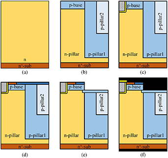
Figures 1(a) and (b) show schematic diagrams of the proposed SJ-MOSFET and the conventional SJ-MOSFET. In figure 1(a), the p-pillar is connected to source (S) via a trench contact on the p+ region. In figure 1(b), the p-pillar is connected to source (S) via a trench contact on the p-type field stop (p-fs) layer, where the p-fs layer has a higher doping than the p-pillar to avoid the punch-through breakdown of the p-pillar. The sidewall of the trench contact connects to the p+ region and p-base region. The ohmic contact on a p-type silicon can be achieved with a wide doping range of 1015 ∼ 1021 cm−3 [24]. As for the Schottky contact, the doping range is about 1015 ∼ 1017 cm−3 [25–27]. So, the contact on the p-base region and p-fs layer can be a Schottky contact or ohmic contact. In the proposed SJ-MOSFET, contact types of the trench contact only have a small influence on electrical characteristics, which will be discussed below. Furthermore, the proposed SJ-MOSFET has a partly relatively lightly doped p-pillar, where a relatively lightly doped p-pillar (p-pillar2) is embedded in the p-pillar1. Such a p-pillar structure can be formed by the double trench filling process with controlled epitaxial speeds of the bottom and the top of the trench [28].

Figure 1. Schematic diagrams of half-cell of (a) the conventional SJ-MOSFET and (b) the proposed SJ-MOSFET with a trench contact on partly relatively lightly doped p-pillar.
Download figure:
Standard image High-resolution imageAt reverse conduction state, since the p-fs layer is thin and has a relatively low doping dose compared to the p-base and p+ regions, electrons can easily inject from the n-pillar into the p-fs layer and be collected by the trench contact, which lowers the hole injection efficiency of the body diode to reduce Qrr. During the reverse recovery stage of current recovering from the peak recovery current (Irrm) to zero, majority carriers in the n/p-pillars are extracted out and the n/p-pillars deplete rapidly in both lateral and vertical directions [22]. As the reason that the p-pillar2 increases the resistance of the hole path, so the extraction of holes in the p-pillar (p-pillar1 and p-pillar2) can be slowed down, which increases the reverse recovery softness and suppresses reverse recovery oscillations.
3. Simulation results and discussion
In Sentaurus TCAD simulations, carrier lifetimes of 1 μs are set. Recombination models of SRH (DopingDependence) and Auger, mobility models of DopingDependent and HighFieldSaturation, impact ionization model of Avalanche (Lackner), bandgap narrowing model of Slotboom, tunneling models of eBarrierTunneling and hBarrierTunneling, and thermionic model are all considered. Table 1 lists key parameters of the conventional SJ-MOSFET and the proposed SJ-MOSFET, where symbols of parameters are given in figure 1. In order to avoid the punch-through of the p-fs layer, Dfs is set to be 1.7 × 1012 cm−2. The contact on the p-base region and p-fs layer is set as a Schottky contact with a barrier height of 0.5 eV.
Table 1. Key parameters of SJ-MOSFETs.
| Parameters | Conv. SJ | Prop. SJ |
|---|---|---|
| ND (cm−3) | 4 × 10¹⁵ | 4 × 10¹⁵ |
| NA (cm−3) | 4 × 10¹⁵ | — |
| Np-base (cm−3) | 2.5 × 10¹⁷ | 2.5 × 10¹⁷ |
| NA1, NA2 (cm−3) | — | 4.8 × 10¹⁵, 1.6 × 10¹⁵ |
| Wn, Wp (μm) | 2, 2 | 2, 2 |
| Tn, Tp (μm) | 37.5, 35.5 | 37.5, — |
| Tp1, Tp2 (μm) | — | 35.5, 17.5 |
| Wp2 (μm) | — | 1 |
| Wfs, Tfs (μm) | — | 2, 0.5 |
| Dfs (cm−2) | — | 1.7 × 10¹² |
| qφbp (eV) | — | 0.5 |
Figure 2 shows forward conducting IVs of the conventional SJ-MOSFET, and two proposed SJ-MOSFETs with a trench Schottky contact and a trench ohmic contact. It can be found that there is almost no difference in the forward conducting IVs of the two proposed SJ-MOSFETs with a trench Schottky contact and with a trench ohmic contact. VB of the proposed SJ-MOSFET (707 V) is a little lower than that of the conventional SJ-MOSFET (727 V). Furthermore, Ron,sp (at JDS = 100 A cm−2 and VGS = 10 V) of the proposed SJ-MOSFET and the conventional SJ-MOSFET are both 12.5 mΩ cm2.

Figure 2. Forward conducting IVs of SJ-MOSFETs.
Download figure:
Standard image High-resolution imageFigure 3(a) shows reverse conducting IVs and current flowlines distributions at JSD = 100 A cm−2 of the conventional SJ-MOSFET, and two proposed SJ-MOSFETs with a trench Schottky contact and a trench ohmic contact. Figure 3(b) shows hole distributions along x = 4 μm at 100 A cm−2 of SJ-MOSFETs. It can be learned from current flowlines distributions that electron current is almost equal to hole current in the conventional SJ-MOSFET, but the conduction current is mainly composed of electron current in the proposed SJ-MOSFET with a trench Schottky contact. This means the hole injection efficiency of the source side of the proposed SJ-MOSFET with a trench Schottky contact is lower than the conventional SJ-MOSFET. Therefore, it can be found in figure 3(b) that the carrier-storage in the p-pillars of the proposed SJ-MOSFET is much lower than the conventional SJ-MOSFET, especially at the top part. Besides, it can be found in figure 3 that the reverse conducting IVs and carrier distributions of the two proposed SJ-MOSFETs with a trench Schottky contact and with a trench ohmic contact are very close. Note that, when electrons inject from the n-pillar into the p-fs layer, electrons flow into the trench contact by diffusing and the electron current mainly depends on the electron concentration gradient in the p-fs layer. Whether the trench contact type is Schottky or ohmic, electron concentrations at the trench contact of these two cases are both negligible. So the effects of the trench contact type on the body diode's electrical characteristics are small, which indicates that the process control of the contact type of the trench contact is not important in the proposed SJ-MOSFET. The small effect is mainly originated from that the built-in potential of the Schottky contact depletes a width of p-fs layer to slightly reduce the effective doping dose of the p-fs layer, which leads to a slightly reduction in carrier-storage in the p-pillars. So, in the discussions below, the proposed SJ-MOSFET with a trench Schottky contact is used to compare with the conventional SJ-MOSFET.

Figure 3. (a) Reverse conducting IVs and current flowlines distributions at JSD = 100 A cm−2. (b) Hole distributions along x = 4 μm at JSD = 100 A cm−2.
Download figure:
Standard image High-resolution imageFigure 4 shows reverse recovery waveforms of body diodes of SJ-MOSFETs under di/dt = 175 A μs−1, where the proposed SJ-MOSFET with NA1/NA2= 1 is the case with uniform doped p-pillar. The devices under test have a same area of 0.2 cm2. The Qrr of the conventional SJ-MOSFET is 2.69 μC and reverse recovery oscillations are particularly significant. The Qrr of the proposed SJ-MOSFET is 1.46 μC, which is reduced by 46%. The tr (the time from t2 to t3) and dir/dt of the conventional SJ-MOSFET are 6 ns and 4887 A μs−1, respectively. The tr and dir/dt of the proposed SJ-MOSFET are 25 ns and 839 A μs−1, respectively. It can be seen that reverse recovery oscillations can be significantly suppressed by using partly relatively lightly doped p-pillar to replace the uniform doped p-pillar.
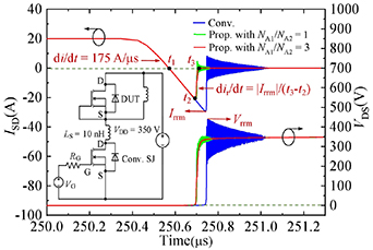
Figure 4. Reverse recovery waveforms of body diodes.
Download figure:
Standard image High-resolution imageIn order to understand the mechanism of suppressing reverse recovery oscillations for the proposed SJ-MOSFETs, figure 5 picks reverse recovery current waveforms of the proposed SJ-MOSFETs during t2− t3 from figure 4. Five points in time (ta1− ta5) for the case with NA1/NA2 = 1 and six points in time (tb1− tb6) for the case with NA1/NA2 = 3 are selected for comparison in figure 5.

Figure 5. Reverse recovery current waveforms of body diodes of the proposed SJ-MOSFETs from the peak recovery current (Irrm) to zero (during t2 − t3).
Download figure:
Standard image High-resolution imageFigures 6(a) and (b) show distributions of hole density and current flowlines for the cases with NA1/NA2 = 1 and NA1/NA2 = 3 during t2− t3, respectively. In figure 6(a), the n-pillar and p-pillar of the conventional SJ-MOSFET begin to laterally deplete at ta1, and then only very few holes store in the p-pillar at ta3, which leads to a rapid current recovery during ta3− ta5. In the conventional SJ-MOSFET, extraction of holes in the p-pillar is almost unobstructed in the hole path. However, the hole path of the proposed SJ-MOSFET can be obstructed during t2− t3. For the case with NA1/NA2 = 3, the process of the reverse recovery stage of current recovering from Irrm to zero can be divided into two stages. During the first stage (tb1 − tb3), part of holes stored in the p-pillar will be extracted quickly via both the p-pillar1 and p-pillar2. At tb3, the p-pillar2 has been depleted due to its relatively low doping concentration, whereas a part of the p-pillar1 has not been almost depleted, storing some holes in the p-pillar1. So, during the second stage (tb3 − tb6), these holes must pass through the almost depleted p-pillar2, which is high-resistance or obstructed for the holes extraction. Therefore, the second state is slower than the first stage and has a positive impact on decreasing dir/dt.
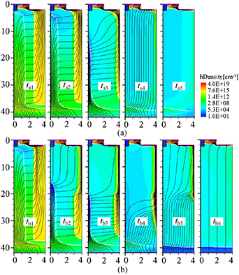
Figure 6. Distributions of hole density and current flow lines with NA1/NA2 = 1 and NA1/NA2 = 3 during t2 − t3.
Download figure:
Standard image High-resolution imageFigure 7 shows effects of Tp2/Tp1 on VB and dir/dt for the proposed SJ-MOSFET, where the total impurities in the whole p-pillar (p-pillar1 and p-pillar2) and Tp1 are unchanged when values of Tp2/Tp1 and NA1/NA2 vary. As shown in figure 7(a), a high NA1/NA2 will significantly reduce VB. When Tp2/Tp1 is about 0.75 (Tp2 = 26.5 μm), VB drops to a minimum valve. Because the electric field distribution is the most uneven in this case due to the non-uniformity of impurity distribution in the whole p-pillar, and the electric field at the bottom of p-pillar1 is higher than other cases. When NA1/NA2 = 3 and Tp2/Tp1 ≈ 0.5 (Tp2 = 17.5 μm), VB = 707 V is acceptable, which is a little lower than that of the conventional SJ-MOSFET (727 V). In figure 7(b), when Tp2/Tp1 increases from 0 to 0.6, dir/dt decreases due to the increase of the resistance of p-pillar2. However, when Tp2/Tp1 increases from 0.6 to 1, the number of remaining holes which stored in the bottom part of the p-pillar1 at the second stage (tb3− tb6 in figure 6) is also reduced. Therefore the extraction of these holes at the second stage will become faster, which causes dir/dt to increase. When Tp2/Tp1 is about 0.6 (Tp2 = 22 μm), the optimal trade-off between the resistance of p-pillar2 and the number of remaining holes can be obtained, which leads to the lowest dir/dt. Considering both VB and dir/dt, it can be found by figure 7 that the optimal design can be obtained when Tp2/Tp1 = 0.5 ∼ 0.6 and NA1/NA2 = 3.
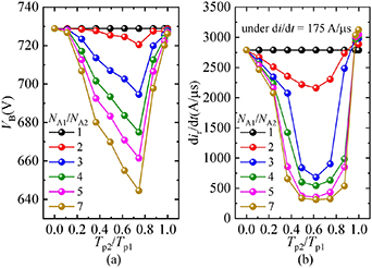
Figure 7. Effects of Tp2/Tp1 on (a) VB and (b) dir/dt.
Download figure:
Standard image High-resolution imageFigure 8 shows effects of di/dt on dir/dt and Vrrm. In figure 8(a), dir/dt and di/dt show a positive correlation trend. When Tp2/Tp1 increases from 0 to 0.5, dir/dt decreases by about 70% under di/dt = 175 A μs−1. In figure 8(b), Vrrm at Tp2/Tp1 = 0.5 is significantly lower than the other two. When Tp2/Tp1 increases from 0 to 0.5, Vrrm decreases by 64 V under di/dt = 350 A μs−1.
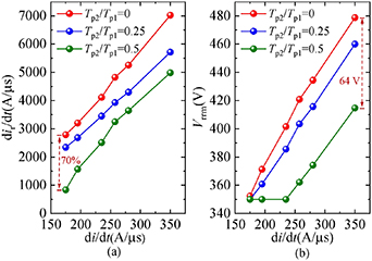
Figure 8. Effects of di/dt on (a) dir/dt and (b) Vrrm.
Download figure:
Standard image High-resolution imageFigure 9 shows effects of Dfs on VB and Jleak (leakage current density at 600 V), where peak doping concentrations of p-fs layer (Nfs) corresponding to values of Dfs have been given out. In order to avoid the punch-through of the p-fs layer, Dfs ⩾ εs E/q should be satisfied, where E is the maximum electric field at the p-fs/p-pillar interface under VB. Simulation results show that E is about 2.25 × 10⁵ V cm−1. Thus, Dfs should be ⩾1.5 × 1012 cm−2. With the decrease of Dfs, VB is not sensitive, but Jleak increases significantly. When Dfs > 1.5 × 1012 cm−2, the p-fs layer is not completely depleted under high blocking voltage. Holes generated in the depleted n-pillar and p-pillar can flow into the source via p-fs layer, p-base region and p+ region in turn. However, when Dfs ⩽ 1.5 × 1012 cm−2, the p-fs layer can be completely depleted, namely, the base region of the n-pillar/p-fs/Schottky contact transistor can be punched through, which results in the increase of Jleak.

Figure 9. Effects of Dfs on VB and Jleak, and distributions of electric field and current flow lines at VDS = 600 V.
Download figure:
Standard image High-resolution imageFigure 10 shows effects of Dfs and Wfs on Qrr and peak reverse recovery voltage (Vrrm) for the two proposed SJ-MOSFETs with a trench Schottky contact and a trench ohmic contact. It can be found that the type of the trench contact has only a small effect on Qrr and Vrrm, where the differences in Qrr and Vrrm between two types of the trench contact are less than 5%. In figure 10(a), when Dfs decreases from 5 × 1012 cm−2 to 1.7 × 1012 cm−2, Qrr is decreased by about 16% under di/dt = 175 and 280 A μs−1, and Vrrm is decreased by about 24 V under di/dt = 280 A μs−1. In figure 10(b), when Wfs is increased from 0.5–2.0 μm, the hole injection efficiency of the body diode can be reduced, which makes Qrr be decreased by about 21% under di/dt = 175 and 280 A μs−1, and makes Vrrm be decreased by about 35 V under di/dt = 280 A μs−1. As for a half cell of the proposed SJ-MOSFET, the widths of the p+ region and the n+ region are both 0.5 μm when Wfs = 2.5 μm, which are relatively extreme values in actual fabrication process for power semiconductor devices. Besides, as mentioned above, Dfs should be ⩾1.5 ×1012 cm−2 to avoid the punch-through of the p-fs layer. Therefore, the device can obtain the optimum performance when Dfs = 1.5 × 1012 cm−2 and Wfs = 2.5 μm.
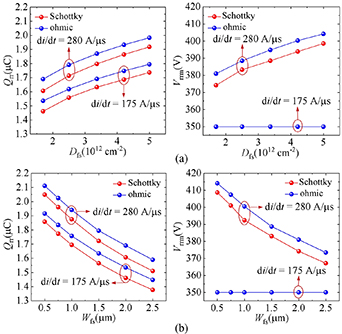
Figure 10. Effects of (a) Dfs and (b) Wfs on Qrr and Vrrm.
Download figure:
Standard image High-resolution imageTable 2 compares performances of the conventional SJ-MOSFET, the proposed SJ-MOSFET, and the SJ-MOSFETs in [16] and [23]. The figure of merit of VB 2/Ron.sp [29] of the proposed SJ-MOSFET is a little lower than the SJ-MOSFET with nine multi-epi layers in [23] but a little higher than that of the SJ-MOSFET with a p-type Schottky contact and a n-type Schottky contact in [16] and the SJ-MOSFET with six multi-epi layers in [23]. Besides, VRC (reverse conduction voltage at JSD = 100 A cm−2) of these SJ-MOSFETs is similar. The SJ-MOSFETs in [16, 23] have a lower Qrr than the proposed SJ-MOSFET. However, the MOS controlled diode in [23] needs extra fabrication steps, and the leakage current of the SJ-MOSFET in [16] is sensitive to temperature since its n-type Schottky contact is reverse biased in the blocking state. As for the proposed SJ-MOSFET, its structure is simpler than the SJ-MOSFET in [23], and its p-type Schottky contact is zero biased or slightly forward biased in the blocking state, which do not affect the leakage current.
Table 2. Comparisons of SJ-MOSFETs.
| Conv. | Prop. | [16] | [23] | [23] | Unit | |
|---|---|---|---|---|---|---|
| Layers | — | — | — | 6 | 9 | — |
| Ron,sp | 12.5 | 12.5 | 17.1 | 14.6 | 10.4 | mΩ·cm2 |
| VB | 727 | 707 | 732 | 697 | 685 | V |
| VB 2/Ron,sp | 42.3 | 40.0 | 31.3 | 33.3 | 45.1 | MW/cm2 |
| Qrr/Area | 13.5 | 7.3 | 5.3 | 5.9 | 5.9 | μC cm−2 |
| VRC | 0.82 | 0.82 | 0.86 | 0.83 | 0.83 | V |
Figure 11 shows feasible process flows of the proposed SJ-MOSFET with NA1/NA2 = 3 and Tp2 = 17.5 μm. The process simulation is as follows.
- (a)Grow a 44 μm n-epi layer with doping concentration of 4 × 1015 cm−3 on an n+-sub.
- (b)Form the p-base doping by boron implantation with dose of 4 × 1013 cm−2 and energy of 100 keV, and diffuse under 1150 °C for 50 min. Then, form the p-pillar1 by etching 38 μm silicon and filling p-type silicon with doping concentration of 4.8 × 1015 cm−3, form the p-pillar2 by etching 20 μm silicon and filling p-type silicon with doping concentration of 1.6 × 1015 cm−3.
- (c)Form the trench gate by etching trench, growing under 1000 °C for 75 min etching sacrifice oxide, growing 100 nm gate oxide (under 1000 °C for 125 min), filling polysilicon and etching polysilicon.
- (d)Form the n+ doping by arisen implantation, and form the p+ doping by boron implantation.
- (e)Form the p-fs layer by etching 2 μm silicon and vertical boron implantations with dose of 2 × 1012 cm−2 and energy of 20 keV.
- (f)Finish metallization.
Figure 11. Feasible process flows of the proposed SJ-MOSFET.
Download figure:
Standard image High-resolution image
4. Conclusion
An SJ-MOSFET with a trench contact on partly relatively lightly doped p-pillar is proposed and demonstrated by TCAD simulations. At reverse conduction state, the hole injection efficiency of the body diode can be lowered by employed trench contact, which helps to obtain an ultralow Qrr. Besides, the resistance of partly relatively lightly doped p-pillar is larger than a uniformly doped p-pillar, which contributes to suppressing reverse recovery oscillations of the body diode. Simulation results show that Qrr of the proposed SJ-MOSFET is 46% lower than the conventional SJ-MOSFET and reverse recovery oscillations can be significantly suppressed. In addition, there is a trade-off between VB and dir/dt and the optimal design can be obtained by adjusting values of Tp2 and NA1/NA2.
Acknowledgments
This work was supported in part by the National Natural Science Foundation of China under Grant 61804101, and in part by the Science and Technology Plan Project of Sichuan Province under Grant 2020YJ0005.
Data availability statement
The data that support the findings of this study are available upon reasonable request from the authors.