

Abstract
Nonlocal quasiparticle transport in normal-superconductor-normal (NSN) hybrid structures probes sub-gap states in the proximity region and is especially attractive in the context of Majorana research. Conductance measurement provides only partial information about nonlocal response composed from both electron-like and hole-like quasiparticle excitations. In this work, we show how a nonlocal shot noise measurement delivers a missing puzzle piece in NSN InAs nanowire-based devices. We demonstrate that in a trivial superconducting phase quasiparticle response is practically charge-neutral, dominated by the heat transport component with a thermal conductance being on the order of conductance quantum. This is qualitatively explained by numerous Andreev reflections of a diffusing quasiparticle, that makes its charge completely uncertain. Consistently, strong fluctuations and sign reversal are observed in the sub-gap nonlocal conductance, including occasional Andreev rectification signals. Our results prove conductance and noise as complementary measurements to characterize quasiparticle transport in superconducting proximity devices.
Export citation and abstract BibTeX RIS
This article was updated on 13 November 2021 to fix a technical error which omitted the supplementary data. The supplementary data for the paper is now available.
Nonlocal conductance measurements [1] in semiconductor-superconductor proximity structures gain renewed interest in the context of Majorana research [2–8]. The key underlying idea is that the nonlocal signals can probe global sub-gap states characteristic of a true topological phase transition [9–11]. This is in contrast to a standard two-terminal conductance [12–14] sensitive to the states near the point where the current inflows in the proximity region. Recent experiments in three-terminal NSN nanowire-based (NW-based) hybrid devices confirm conceptual power of the nonlocal conductance approach [15, 16].
Conductance measurement provides only partial information about quasiparticle non-equilibrium in proximity structures. A sub-gap quasiparticle entering the proximity region carries the electric charge,  for electron-like and
  for hole-like quasiparticles, and the excitation energy
  , where E is the kinetic energy relative to the chemical potential of the superconductor. On its way, apart from possible normal scattering, a quasiparticle experiences a few Andreev reflections (ARs) from the superconducting lead [17, 18], each time inverting the q but preserving the ε. Thereby, the AR mediates a coupling of the charge and heat (energy) transport components that is unique to proximity structures and does not occur in bulk superconductors [19, 20]. Thus, a full characterization of the non-equilibrium can be achieved by a measurement of both the electric and heat nonlocal conductances.
In this article, we investigate the nonlocal response in NSN InAs NW-based devices. We show that a quasiparticle non-equilibrium can be understood if the nonlocal conductance is accompanied by a shot noise measurement substituting the heat conductance measurement, that allows to separate the contributions of transmission processes involving even and odd number of the ARs. Experiments performed in a trivial superconducting phase demonstrate that quasiparticle transport is practically charge-neutral, so that the heat transport component dominates the nonlocal response in our devices. Our results prove shot noise as a valuable, complementary to conductance, tool to probe the sub-gap states in proximity structures.
We start the discussion from the energy diagram of the NSN NW-based hybrid structure in a nonlocal experiment sketched in figure 1(a). Consider the case of zero temperature T = 0 and negative bias voltage  applied to the left normal terminal
  . The superconductor and the right normal terminal
  are grounded, position of their chemical potential shown by the dashed line. Transmitted quasiparticles are distinguished by their energy relative to this chemical potential,
  for electrons and −ε for holes. Inside the NW quasiparticles experience ARs from the S-lead and elastic normal scattering from disorder and possibly from the S/NW interface, inelastic scattering is absent [21]. The charge current
  and the heat current
  in the right lead read [22, 23]:

where the positive direction for the electric current is from the lead into the scattering region and opposite for the heat current.  and
and  are the probabilities of transmission, respectively, preserving and changing a quasiparticle type, sometimes also called normal and crossed-Andreev transmission [6] and the sum over the eigenchannels is performed. Generally, the two transmission processes involve both the normal and Andreev scattering and are distinguished by the parity of the number of ARs involved. Processes with an even and odd number of ARs contribute, respectively, to
  and
and  . Equations (1) imply that a simultaneous measurement of the charge and heat response permits an independent characterization of
  and
and  . Measurement of the heat transport is not an easy task [24–27] and we choose a different path in the present experiment. We perform a shot noise measurement in a nonlocal configuration [21, 28, 29], based on the findings of [11] briefly mentioned below.
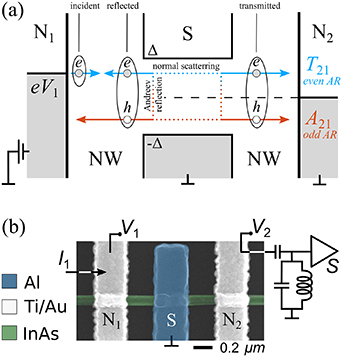
Figure 1. (a) Energy diagram of the NSN NW-based device. In this illustration, the left normal terminal N1 is biased with voltage  , while the central S-terminal and the right N2 terminal are grounded, their chemical potential shown by the dashed line. Depending on the number of Andreev reflections, the electron incident from N1 can be transmitted towards N2 as an electron (e) or hole (h) with probability
  or
or  correspondingly. (b) Scanning electron microscope image of the NSN-II device (false color) and the shot-noise measurement scheme used in actual experiment. Voltages V1 and V2 that build up in response to the current bias I1 are measured in a quasi-four-terminal configuration.
Download figure:
Standard image High-resolution imageThe average charge  (in units of e) transmitted in one eigenchannel in an individual scattering event equals
  . Its fluctuation is
  , where
  . Thus, in the spirit of [30], we obtain for the spectral density of the current noise in the right lead:
that contains  and can substitute
  in a nonlocal measurement. In the limit of suppressed AR
  equation (2) reduces to a familiar result in the normal case [31]. In this case, a nonlocal Fano factor defined as
  is bounded by unity
  . In the opposite limit of
  the shot noise and the heat current remain finite,
  , whereas
  . Here, the nonlocal quasiparticle response is charge-neutral and
  .
.
Equations (1) and (2) illustrate our main idea that nonlocal conductance  and shot noise S2 can serve as two complementary electrical measurements required to fully characterize quasiparticle transport. We apply this paradigm to explore the nonlocal response in InAs NW-based NSN devices. The outline of the experiment is depicted in figure 1(b). A semiconducting InAs nanowire is equipped with an S terminal, made of Al, in the middle and two N terminals, made of Ti/Au bilayer, on the sides. In essence, this device represents two back-to-back N-NW-S junctions sharing the same S terminal. We study two similar devices, NSN-I and NSN-II, which have the width of S terminal equal to
  and
and  , respectively. Note the absence of the plunger gates, typically used to define the quantum dots [32–34] or tunnel barriers [35] adjacent to the S-terminal. In addition, for all contacts in-situ Ar milling was applied before the evaporation in order to improve the semiconductor/metal interface quality. All of this enables better coupling of the sub-gap states to the normal conducting regions. As a result, the resistances of the individual N-NW-S junctions are mainly determined by disorder scattering rather than unintentional interface reflectivity. This is confirmed by smooth gate voltage characteristics and universal diffusive value of the shot noise Fano factor in the normal state, see the data of the related experiment in [36]. Throughout the experiments the S terminal is grounded, terminal
  is current biased. The terminal
  is DC floating throughout the experiment, which allows to access the differential resistances
  in a quasi-four-terminal configuration excluding the wiring contributions. The differential conductances are obtained by inverting the measured resistance matrix, see the Supplemental Material for the details (available online at stacks.iop.org/SST/36/09LT04/mmedia). In the present experiment, the non-diagonal elements are much smaller than the diagonal ones, so that approximate relations
  and
and  hold within a few percent accuracy. Experiments are performed at bath temperatures of T = 120–150 mK unless stated otherwise.
Back-gate voltage ( ) dependencies of the linear response diagonal conductances are shown in figure 2(a). Gii
fall in the range of a few conductance quanta and exhibit a usual sublinear increase with
) dependencies of the linear response diagonal conductances are shown in figure 2(a). Gii
fall in the range of a few conductance quanta and exhibit a usual sublinear increase with  accompanied by universal mesoscopic fluctuations. Standard procedure [37] gives a field-effect mobility of
  underestimated because of the field screening by contacts. Impact of a superconducting proximity effect on Gii
is similar for both devices and all
underestimated because of the field screening by contacts. Impact of a superconducting proximity effect on Gii
is similar for both devices and all  used, typical data shown in figure 2(b). In zero magnetic field B a moderate zero-bias minimum is seen surrounded by maxima at V = ±Δ/e, where Δ = 180 µeV is the Al superconducting gap, independently determined from the critical temperature, see Supplemental Material. In a uniform magnetic field of B = 50 mT obtained with a superconducting solenoid, oriented perpendicularly to the substrate and high enough to suppress the superconductivity the minimum weakens and the maxima disappear, whereas the above-gap conductance remains unchanged. Overall, this is a standard for coherent diffusive NS junctions re-entrant behaviour [38, 39], with a minor effect of the interface reflectivity and/or Coulomb effects [40].

Figure 2. (a) Zero-bias diagonal conductances versus  for both devices in zero magnetic field. (b) Diagonal differential conductance as a function of bias voltage in zero and high enough to suppress superconductivity magnetic fields. Dotted lines show position of the superconducting gap. (c) and (d) B = 0 nonlocal differential conductance as a function of
  for several
  values. The curves are vertically offset for clarity, with zero level shown by the dashed lines. Bars indicate the ordinate scale common for all
  .
.
Download figure:
Standard image High-resolution imageThe non-diagonal conductance probes quasiparticle transport via InAs-NW section underneath the S-terminal [4, 6, 7, 15, 16] and its bias dependence turns out much less universal. In figures 2(c) and (d) we plot  , having in mind that the negative sign corresponds to normal transmission. At sub-gap biases, very different behaviour of
  can be observed depending on
  , from almost symmetric with zero-bias maximum, see
  V data in device NSN-I, to strongly anti-symmetric with sign inversion, see
  V data in device NSN-II. By contrast, in the normal state
  is negative, featureless and consistent with a current transfer length of ∼ 100 nm determined by a residual interface reflectivity, see the Supplemental Material. Figures 2(c) and (d) show that at sub-gap biases in the superconducting state
  strongly increases compared to its above-gap values, which is expected since quasiparticles are forbidden to enter the superconductor. The
  is much smaller than e2/h and occasionally changes sign, implying that
  and fluctuates around zero as a function of energy and chemical potential. Below we present the nonlocal shot noise experiment that uncovers charge-neutral origin of the quasiparticle transport.
The layout of the shot noise measurement in a nonlocal configuration is sketched in figure 1(b). The current fluctuations are picked up at the floating terminal  in response to the current between the biased terminal
  and the grounded S-terminal. Plotted as a function of V1 all the data in both devices feature the same qualitative behaviour shown in figures 3(a) and (b). The shot noise spectral density S2 starts from the Johnson-Nyquist equilibrium value
  at zero bias [23] and increases almost symmetrically and linear with V1 showing a pronounced downward kink at the gap edges
  marked by vertical dashed lines. Above the gap the slope drops down consistent with the fact that transmission probability diminishes as soon as the quasiparticles can sink in the superconductor. Nonlocal noise is more informative than the usual two-terminal noise in NS structures [33, 41–43], which exhibits only a minor reduction in the presence of sub-gap density of states [44]. According to the equation (2), neglecting the contributions of
  the slope
  is determined by
  and allows to evaluate the linear response thermal conductance
  . We have
  , where
  is the thermal conductance quantum and
  is the Lorenz number. This estimate of
  is legitimate provided
  , i.e. if ballistic transmission is suppressed by disorder scattering [18, 45], as in our devices, or by structure geometry [46]. Note that our results manifest a drastic violation of the Wiedemann-Franz law [47] since a zero resistance of the NW region covered by the superconductor coexists with a relatively small thermal conductance via the sub-gap states.

Figure 3. (a) and (b) Measured current noise spectral density in the right lead as a function of bias voltage on the left one. Dotted lines show positions of the superconducting gap. (c) and (d) Measured current noise spectral density in the right lead as a function of the nonlocal current  . Symbols have the same colour as the lines in panels (a) and (b) for the respective
  . Guide lines with Fano-factor
  and
and  are plotted as dashed and dotted lines correspondingly.
Download figure:
Standard image High-resolution imageNext we analyse the same data in terms of the nonlocal Fano factor, where the nonlocal current is obtained via  . Here we use that the electric current caused by non-equilibrium quasiparticles is compensated by an extra current flowing in the opposite direction, so that the net current is zero in the floating configuration. This extra current flows near the Fermi level and is noiseless, since the junction N2-NW-S remains essentially unbiased throughout the experiment,
  , see the Supplemental Material. Figures 3(c) and (d) plot S2 vs
  for both devices. Two main features are evident. First, the symmetry inherent to S2 vs V1 data is in many cases lost here, since
  is not an anti-symmetric function of V1. Second, the noise slope corresponds to nonlocal Fano factor values in the range
  , as shown by the dotted guide lines. Such giant values of
  rule out a heretical interpretation that normal quasiparticle scattering from a poor quality Al/InAs interface is the main source of nonlocal signals, that would correspond to
  , see the dashed guide line.
It is convenient to define the average charge of transmitted quasiparticles as the ratio between the transmitted charge and total number of transmitted quasiparticles  . The value of
  corresponds to the case when quasiparticles conserve their charge during the transmission process, whereas in the case
  they invert the charge. As follows from the equations (1) and (2),
  , i.e. the observation of a giant Fano factor implies nearly charge-neutral nonlocal quasiparticle transport with
  . This can be easily understood in case of a metallic diffusive NW covered by a superconductor with a transparent interface. Traversing the proximity region a quasiparticle experiences a number of ARs given on the average by
  , where w is the width of the S-terminal and d ≈ 100 nm is the diameter of the NW. Given the randomness of diffusion the mean-square fluctuation is
  , so that the parity of
  and thus the sign of the transmitted charge are completely uncertain. More rigorously, for the device NSN-II we find
  , meaning that it takes at least a hundred quasiparticles to transmit a unit of elementary charge.
Our observations in a trivial superconducting phase have common features with the predicted nonlocal response at the topological phase transition in Majorana NWs. Here, even in presence of a moderate disorder, a finite transmission occurs in just one eigenchannel with  and results in a pure heat transport characterized by a universal peak of the thermal conductance
  [11]. While comparable in absolute value,
  in the present experiment demonstrates a monotonic dependence on
  . The nonlocal charge response at the topological transition restores at a finite bias,
  , owing to the energy-dependence of the transmission probabilities, known as the Andreev rectification [4]. Similar transport features are occasionally observable in figures 2(c) and (d), originating from mesoscopic fluctuations of G21 around zero. This suggests that, unlike the peak in
  , Andreev rectification is not a unique signature of the topological transition, see also [16].
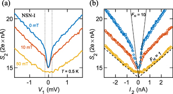
As a final step, we demonstrate a crossover from nearly charge-neutral to normal nonlocal quasiparticle transport in a magnetic field in the device NSN-I. Figure 4(a) shows the evolution of S2 vs V1, taken at a bath temperature of 0.5 K. The shot noise gradually diminishes at increasing B-field and the kink at the gap edge disappears concurrently with a transition of the Al to the normal state, see the B = 50 mT trace. Plotted as a function of  in figure 4(b) this data reveals a transition from the giant noise at sub-gap energies in the B = 0 superconducting state to the Poissonian noise in the normal state, see the dashed guide line. In B = 0 we find
  , considerably diminished compared to figure 3(c) as a result of thermal smearing. The Poissonian noise
  in the normal state corresponds to A21 = 0 and
  , as a result of residual interface scattering. Notably, in the superconducting state the slope corresponds to
  even beyond the kink, see also figures 3(c) and (d), since the probability of the AR remains finite above the gap [19].
Figure 4. (a) Evolution of the nonlocal noise spectral density  in magnetic field and
  . Dotted lines show positions of the superconducting gap. (b) Evolution of the nonlocal noise spectral density
  in magnetic field. Symbols have the same colour as the lines in panel (a) for the respective B. Guide lines with Fano-factor
  and
and  are plotted as dashed and dotted lines correspondingly.
Download figure:
Standard image High-resolution image
In summary, we performed nonlocal transport and noise experiments in InAs NW-based hybrid NSN devices. Such a combination of all-electrical measurements allows to estimate the thermal conductance and reveals a predominantly charge-neutral origin of the nonlocal response. We expect that our approach will be generally useful for the studies of non-equilibrium proximity superconductivity, including unequivocal identification of the topological phase transition in Majorana devices.
We are grateful to A P Higginbotham, T M Klapwijk, A S Melʼnikov and K E Nagaev for helpful discussions. This work was financially supported by the RSF project 19-12-00 326 (fabrication, experiments in NSN-I device) and RFBR project 19-02-00 898 (experiments in NSN-II device). Theoretical framework was developed under the state task of the ISSP RAS. Work at TUM was supported by the Deutsche Forschungsgemeinschaft (DFG) via project KO-4005/5-1 and Germany's Excellence Strategy-EXC-2111-390814868 (Munich Center for Quantum Science and Technology, MCQST).
Data availability statement
The data generated and/or analysed during the current study are not publicly available for legal/ethical reasons but are available from the corresponding author on reasonable request.