

Abstract
Laser patterning has been used for the micro-scale fabrication of semiconductor devices like solar cells, photodetectors, LEDs, and also for modification of surfaces for wettability, reflected colors, initial bacterial adhesion, etc, due to its several advantages of patterning flexibility, spatial resolution, and mask-free operation over complex conventional lithography. Currently, laser-induced ablation is a promising patterning method in silicon solar cell fabrication; however, laser-induced defects, and thermal stresses remain a significant concern. In this paper, we demonstrate a laser ablation-free method for patterning c-Si based on the observation that the anisotropic etching of c-Si by KOH is highly temperature-dependent as the etching rate is about 100 times faster at 80 °C compared to room temperature. The laser heating-induced chemical etching (LHICE) of crystalline silicon can help alleviate such laser-induced damage by providing the necessary low temperature on the localized area(s) on the silicon substrate. We investigated the micro-second pulsed laser-assisted chemical etching of c-Si substrate for microscale patterning and showed that laser-induced damage could be eliminated as indicated by the minority carrier lifetime preservation. We also present results of the effect of laser processing parameters such as laser power, scan speed, and duty cycle on etching depth and surface morphology. The optical, surface morphology, depth profile, and LCPSim simulation results are also presented to optimize and understand the LHICE process. This versatile methodology of temperature-selective chemical etching could be applied to various thin-film and bulk materials used in diverse device fabrication.
Export citation and abstract BibTeX RIS
1. Introduction
As of 2017, the crystalline silicon PV modules accounted for about 90% of the world PV solar cell market share [1]. Currently, the interdigitated back-contact hetero-junction (IBC-HJ) silicon solar cells and the passivated emitter rear contact (PERC) silicon solar cells are very popular for commercial applications due to their higher efficiency and lower manufacturing costs [2–4]. Recently, a record 26.1% efficiency for polycrystalline on oxide junction interdigitated back contact (POLO-IBC) solar cell and 26.3% efficiency for IBC-HJ c-Si solar cell have been reported [4, 5] utilizing a laser ablation patterning method. One of the major issues in using laser processing for Si solar cell fabrications lies in the occurrence of laser-induced defects and thermal stress in the lattices, which eventually lowers down the effective minority carrier lifetime (MCL) and hence, conversion efficiency. Hence, the widespread commercialization of high-efficiency IBC and PERC solar cells depends on the availability of a low-cost laser-patterning method, which ensures minimum laser-induced damage. The isotropic etching of c-Si can be achieved using a mixture of HF (49%) and HNO3 (69%) in the ratio of 1:19 by volume and is widely used in the semiconductor industry [6]. Potassium hydroxide (KOH) and tetramethylammonium hydroxide (TMAH) are widely used to create an anisotropic-etched micro-texture surface on c-Si [7–11].
Recent reports show that by using ultrafast femtosecond (fs), picosecond (ps) lasers, and nanosecond (ns) pulse width lasers combined with anisotropic chemical etching (using KOH and TMAH aqueous solutions), SF6 or HCl gases, or stain etchants (using HF–HNO3, NH4HF2–H2O, NH4HF2–NaMnO4), it has been possible to produce various kinds of micro-and nano-sized structures and microtextures like pores, pillars, porosified pillars, macro-pores, pin-holes and polygonal pits in c-Si using laser ablation process [12–16]. These micro-/nano-structures have been made for the fabrication of photoluminescent porous Si (Poro-Si) [13, 16]; better hydrophobicity and enhanced light-trapping mechanism in c-Si solar cells and self-cleaning c-Si microelectronic devices [14]; controlled reflectance, absorbance, and emissivity of Si-based optical devices [15, 17]. A few other applications of Poro-Si are Li-ion battery anodes [18] and other minority carrier devices like photodetectors, thin-film transistors, and LEDs, etc, where their performances degrade due to carrier traps and defect density [19–21]. But the advantages of such micro-and nano-structures are not just limited to the c-Si based solar cell and micro-electronics devices but also to various materials-based devices for novel purposes like surface super-hydrophobicity and wettability [22, 23], reflected colors [24], tribological behaviors [25], bacterial anti-biofouling [26], etc. According to Ji et al, when the accumulation and transfer of energy from the laser to c-Si reach the phase explosion conditions (>0.9 Tc, Tc = 7925 K, it is the thermodynamic critical temperature of silicon), it leads to an explosion splash of ionized surface material caused by explosive stress, leaving micropores on the silicon surface [14]. Obviously, there were significant defects formed to the surface and bulk of c-Si wafers/ substrates due to the extensive laser ablation process and high-temperature chemical etch in all these processes. As a matter of fact, the effects of the direct laser-crystalline silicon interactions seemed to be dominant over the laser-assisted chemical etch interaction effects. The laser-induced damages were not characterized adequately, and the preservation of MCL was not previously investigated. Additionally, there is a lack of understanding of the role that micro-second (µs) pulse width lasers play in low-temperature laser-assisted KOH etching of c-Si and how it influences the change in the MCL. Several works on laser-assisted photochemical wet etching methods have been reported where the exposure of a particular laser wavelength with an optimized intensity selectively enhances the photochemical etch rate at a localized place and does not depend on the laser heating. However, such a method is limited to only semiconductor materials like c-Si, GaAs since the etching rate depends on the formation of e−h+ pairs and requires toxic etchants like HF [27, 28].
From semiconductor processing, it is well known that the KOH etching rate increases exponentially above the room temperature as described by the Arrhenius equation, and the optimum temperature range lies within 80 °C to 100 °C. The 30 wt% concentrated KOH etch rate of c-Si (100) at 20 °C is ∼1.44 µm h−1 (=24 nm min−1) whereas at 80 °C, the etch rate becomes ∼79 µm h−1 (=1316 nm min−1) [9]. The mechanism of silicon etching by KOH is a two-step sequential oxidation and etching reaction. During the rate-limiting process of oxidation, H-terminated Si atoms at the surface get oxidized to OH-terminated Si atoms due to OH- ions from KOH aqueous solution. In the presence of H2O, polarization and weakening of the back bonds occur due to differences in electronegativity between Si and O. Consequently, etching (removal) of Si atoms occurs in the form of Si(OH)4 complexes [29]. The rate-limiting oxidation process can be accelerated by an optimal temperature range from 80 °C to 100 °C. Moreover, it is a non-toxic, economical, and commonly used alkali metal hydroxide silicon etchant, which requires a simple etch setup and provides high silicon etch rate, a high degree of anisotropy, moderate Si/SiO2 etch rate ratio, and low etched surface roughness.
Generally, the prime goal of creating textures and pyramidal shapes on a c-Si surface has been to enhance light trapping, using alkaline KOH, NaOH, and TMAH, ensuring surface reflectivity as low as 6% [30]. The KOH etching/ texturizing of c-Si does not cause any major damage to the surface quality, and the surface passivation on the etched/textured c-Si can be further improved by the deposition of SiO2/Al2O3 and SiNx/Al2O3 stack layers [31–33]. The surface passivation, as in IBC solar cell fabrication, can also be done by depositing the PECVD stack of a-Si /SiO2 /SiNx (aSON) layers on the textured c-Si to obtain effective surface recombination velocities (SRVs) below 1 cm s−1 [34]. Zielke et al reported that a very low saturation current density of (174 ± 11) fA cm−2 was measured on the PERC cells after KOH pyramidal texturization, followed by atomic-layer-deposited AlOx , indicating better contact passivation [35]. The report by Werner et al shows that it has been possible to achieve a low SRV below 2.9 cm s−1 with a 10 nm thick Al2O3 layer, deposited by spatial ALD process, on a KOH-etched n-type Czochralski-grown (Cz) silicon [36]. Hence, an optimum temperature range (80 °C to 100 °C) has to be achieved, which would suffice for KOH etching/texturization. Similar laser-assisted temperature-selective micro-etch/ texturization is quite feasible for controlled etching steel in etchant FeCl3 and aqueous solution mixture of FeCl3/ HCl/ HNO3 for super-hydrophobicity, wettability and surface-reflected colors [23, 24, 37, 38], Ni–Co alloys on steel in etchant 30% v/v HCl/ethyl alcohol for tribological properties [25, 39] and many more. Moreover, such methodology can also overtake the extensive electrochemical etching for Poro-Si texturization, which eventually lowers down the carrier lifetime [40].
In this paper, we describe a highly localized micron-resolution patterning using a micro-second (µs) pulsed laser based on the laser heating-induced chemical etching (LHICE) process, where the carrier lifetime is preserved. This methodology's fundamental approach lies in the increase in the temperature at localized areas irradiated by laser and enhancing the forward reaction rate of temperature-dependent chemical etching of c-Si. Hence, by proper selection of laser processing parameters, the patterning of c-Si was achieved, and no direct ablation by laser was required. Such a temperature regime was considered low and safe for silicon solar cell fabrication. Consequently, the direct laser-induced defects and thermal stresses in the c-Si lattice were minimized.
After using microsecond pulse-width laser-heated KOH etch patterning of c-Si, we investigated the effect on MCL. Analytical techniques like optical microscopy, scanning electron microscopy (SEM), Sinton QSSPCD MCL measurement, white-light Zygo optical profilometry, and LCPSim simulation were used for characterizations to understand the laser-assisted chemical etching process. This low-cost, low-temperature patterning method will find other applications in a variety of solar cell designs based on inorganic and organic materials, and the availability of such a method for the fabrication of high-efficiency solar cells will greatly help the solar industry. It will also be applicable to a variety of other materials like metals, ceramics, and semiconductors.
2. Experimental
The laser used in the experiment was IPG Photonics YLR-150/1500-QCW-AC-Y11 with a wavelength of 1070 ± 5 nm operating at quasi-continuous mode. The pulse energy was ∼1.5 J with a maximum peak power of 1500 W. The laser repetition rate was kept constant at 500 Hz. To study the effects of duty cycles on LHICE, the laser pulse widths were 100 µs, 150 µs, 200 µs, and 250 µs. Hence, the corresponding duty cycles were 5%, 7.5%, 10% and 12.5% respectively. In order to study the effects of the laser scan speeds on LHICE, the scan speeds of 10 mm s−1, 15 mm s−1, and 50 mm s−1 were used. To investigate the effect of laser power, the average laser powers of 14.1 W, 16.4 W, 18.6 W, and 21 W were used. The laser spot size was fixed at ∼430 µm at FWHM at the focal plane, and the total scan number was kept constant at 4.
The double-side polished n-doped FZ c-Si <100> type wafer with a thickness of 300 µm and 1–5 Ω cm resistivity was used for the experiments. The c-Si wafer was cut into a 1 × 1 inch size sample and then cleaned with methanol and HF solutions to get rid of surface contaminants. A total of nine straight parallel lines were patterned, quite similar to the pattern used by Sinha et al [41], each 13 mm long and separated by gaps of ∼500 µm in between while keeping it immersed in a 30 wt% concentration of KOH alkaline solution in a polystyrene petri dish. The petri dish was filled up to 1 mm in the height of the KOH solution above the wafer. The schematic diagram of the experimental setup is shown in figure 1. The MCL was measured before and after the laser processing using a chemical passivation technique of 0.08 mol l−1 concentration of I2-methanol solution [42]. The investigative analysis was further carried out using optical microscopy, SEM, white-light Zygo optical profilometry, and LCPSim simulation [43].

Figure 1. Schematic diagram of the experimental setup.
Download figure:
Standard image High-resolution imageThe optical images were taken using a Hirox 3D Digital Microscope. The QSSPCD MCL was measured using WCT-120 Silicon Wafer Lifetime Tester made by Sinton Instruments. The surface morphology was characterized using an FEI Quanta 650 Field Emission Scanning Electron Microscope, and the depth profiles were measured using the white-light optical profilometer Zygo NewView 7300.
3. Results and discussions
3.1. Influence of laser processing parameters, surfactant, and solution stirring
The understanding of the effects of various laser processing parameters like laser scan speed, duty cycle, and laser power on the surface morphology is essential for laser-patterning optimization. In addition to that, the effects of the usage of surfactant and solution stirring process were examined. The non-destructive white-light Zygo optical profilometry was used for the characterization of all the depth profiles of the laser-assisted etched groove lines under these different conditions.
3.1.1. The effect of laser scan speed variation.
The effect of laser scan speed on LHICE was investigated. From figures 2(a)–(c), it was observed that at a constant average power of 18.6 W and 5% duty cycle, the etch depth increased from ∼25 nm to 135 nm as the scan speed was reduced from 50 mm s−1 to 10 mm s−1. Lower scan speed corresponded to the higher number of laser pulses, and hence, more heating occurred, which resulted in deeper etchings. The depth-color maps show distinct groove features with increasing etch depth as the scan speed was reduced, as shown in figures 2(d)–(f). But as the scan speed was reduced below 10 mm s−1, excessive heating occurred, which resulted in direct evaporation of KOH and laser-induced ablations of the c-Si.

Figure 2. Zygo profilometry showing the surface profile of laser-induced KOH etched lines on the c-Si substrate at scan speed (a) 50 mm s−1, (b) 15 mm s−1, and (c) 10 mm s−1, respectively while keeping other parameters constant. The figures(d)–(f) show the depth-color mapping images of the lines corresponding to the scan speeds of 50, 15, and 10 mm s−1, respectively.
Download figure:
Standard image High-resolution imageThe color map also proves that there is negligible impact outside the desired etched region, and the process was highly spatially localized. Laser processing in a liquid etchant medium is different from laser processing in air/vacuum. From the literature, it is known that the lattice thermal conductivity of c-Si (∼5.1 W (m K)−1) is greater than the thermal conductivities of 30 wt% KOH (∼0.727 W (m K)−1) and air (∼0.02–0.03 W (m K)−1) [44–46]. Hence, much of the laser-induced heat is redistributed within the c-Si lattice and a small amount of the heat gets dissipated out to an immediate liquid etchant medium. This results in the heating of the liquid surrounding the laser-irradiated region on c-Si. Figure 3 shows the top-view SEM image of a laser-assisted KOH etched line on the c-Si substrate at a scan speed of 15 mm s−1. The average width of the etched groove line was found to be ∼280 ± 10 µm. The SEM results indicate that the localized laser-induced heat was responsible for the KOH-etched groove and not the direct laser ablation and stress. The laser power was low enough not to cause direct melting of the silicon surface. Minor turmoil and boiling of the etchant liquid near the Si surface caused the groove boundaries to be slightly irregular. Too high a laser power will cause melting of silicon, a significant amount of bubble formation and vaporization and would lead to uncontrolled etching.

Figure 3. Top-view SEM image of the laser-induced KOH etched lines obtained under the scan speed 15 mm s−1.
Download figure:
Standard image High-resolution image3.1.2. The effect of laser duty cycle.
Figures 4(a)–(c) show an increasing etch depth from ∼25 nm to 80 nm and groove line-width increase from ∼150 µm to 350 µm as the duty cycle was increased from 5% to 10%. For constant laser average power and scan speed, the shorter pulse-width caused higher peak energy per pulse, resulting in limited etching even though the laser-induced temperature was quite high. As the duty cycle increased, the pulse-width increased, which caused a longer heating duration. Consequently, more time was available for KOH chemical reaction to occur, resulting in deeper etch depth and wider groove lines. Thus, the duty cycle was found to be an important factor influencing the LHICE method. The LCPSim simulation model, discussed in the later section, also proved the importance of a longer duration of heating and a larger duty cycle.

Figure 4. Zygo profilometry showing the surface profile of the KOH-etched groove lines at various laser duty cycles (a) 5%, (b) 7.5%, and (c) 10% while keeping average power (18.6 W) and scan speed (50 mm s−1) constant.
Download figure:
Standard image High-resolution image3.1.3. The effect of laser power variation.
The results of the influence of varying average laser power while keeping 7.5% duty cycle and a scan speed of 50 mm s−1 are shown in figures 5(a)–(c). As the average laser power was increased from 14.1 W to 18.6 W, there was a small increase in the etch depth. Although the etch depth increase was not that significant, but the groove lines widened. Average power lower than 14.1 W did not create any etch grooves and average power higher than 18.6 W caused direct laser ablation of silicon, as shown in figure 6. So, it was concluded that the average power solely could not determine to etch depth in LHICE.
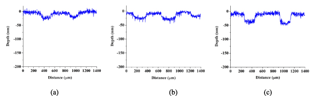
Figure 5. Zygo profilometry showing the surface profile of the KOH-etched groove lines at various average laser powers (a) 14.1 W, (b) 16.4 W, and (c) 18.6 W while keeping other parameters constant (duty cycle = 7.5% and scan speed = 50 mm s−1).
Download figure:
Standard image High-resolution image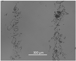
Figure 6. Optical image showing the laser-induced ablation at an average power of 21 W.
Download figure:
Standard image High-resolution image3.1.4. The effect of using surfactant and solution stirring.
The surfactant Triton X-100 is generally used for improving surface wetting during KOH etching of c-Si. A 100 ppm of Triton X-100 was added to 30% KOH solution. Figures 7(a) and (b) show the etch depth for KOH solution with and without surfactant. It was found that under constant average power of 18.6 W, 5% duty cycle, and a scan speed of 10 mm s−1, the sample etched with Triton containing KOH had shallower etch depth (∼75 nm) than the one etched with only KOH (∼130 nm). The etching rate was found to be slower in the case of Triton-added KOH etch, but the average roughness improved from 36 nm to 20 nm. Similar lower etch rates and smoothening effects of Triton addition to KOH etchant had been shown earlier by Rola et al [47].
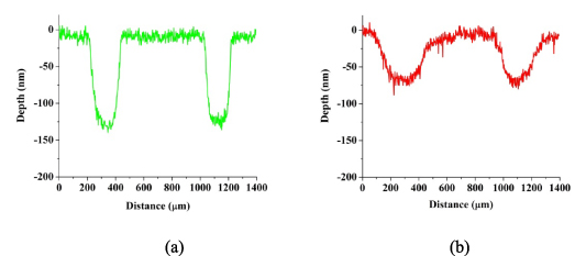
Figure 7. Zygo profilometry showing the surface profile of the KOH-etched groove lines (a) without Triton X-100 and (b) with Triton X-100 while keeping all laser parameters constant (duty cycle = 5% and scan speed = 10 mm s−1).
Download figure:
Standard image High-resolution imageIn order to remove bubbles formed during heating, solution stirring was attempted using a magnetic stirrer, rotating at 50–100 rpm. The liquid stirring caused an increase in unwanted turbulences on the liquid surface. This led to the irregularity in etch depth due to the higher scattering of the laser beam.
3.1.5. Reproducibility and scalability.
Reproducibility and scalability are the important factors that determine its reliability and industrial application. Three identical samples were etched using the same laser parameter conditions. From figure 8, it is observed that using average power of 18.6 W, 5% duty cycle and a scan speed of 15 mm s−1, similar etch depth (∼110 ± 10 nm) and width (∼300 ± 20 nm) were obtained. So, the LHICE process is reproducible and reliable.

Figure 8. Zygo profilometry showing the reproducibility of the etch depths in three different 1 × 1 inch c-Si samples using the same laser parameters: average power 18.6 W, 5% duty cycle, and scan speed of 15 mm s−1.
Download figure:
Standard image High-resolution image3.1.6. The effect of laser-assisted chemical etch time.
The silicon etching rate is dependent on KOH concentration and temperature. In our study, KOH concentration was fixed at 30 wt%. The etching rate initially increases with concentration and then decreases. So, it may be possible to choose higher KOH concentration which will allow increase in the boiling point of the solution and lower etching of the laser untreated area [48].
The applicability of the LHICE process should fulfill the short time criterion to achieve high throughput in the solar cell industry. Commercially, 6 × 6 inch silicon solar cells are quite dominant in the market, and hence, selective laser-assisted KOH etching of 6 × 6 inch c-Si wafers must be a time-efficient process.
The approximate time taken to pattern four scans of a single 13 mm straight line was 1.65 s to obtain ∼110 ± 10 nm groove depth. Hence, the total time taken to pattern nine such parallel patterns was 14.85 s. The time taken for a complete selective laser-assisted KOH etching of c-Si samples can be improved by an optimized combination of multiple-beam systems, spot size, KOH concentration, average laser power, pulse width, laser wavelength, and the number of laser scans. So, to draw a single 6 inches (i.e. 152.4 mm) line pattern on a 6 inch wafer with four scans and similar groove depth, it would take 18.9 s. To create each etched line of ∼20 nm etch depth, it would take approx. 4 s. The amount of etched depth can be chosen according to the industry needs. By using a multiple beam system, it is possible to shorten the large-area processing time further. Instead of using circular laser beams, one-dimension line beams can be used to generate faster uniform line patterns. By using higher power lasers, the focused laser beamline length can be made longer than used in our experiments, which will allow much faster throughput.
3.2. QSSPCD carrier lifetime characterization of semiconductor c-Si
QSSPCD characterization tool is useful to investigate the extent of damages and defects on the surface and bulk of the c-Si substrate after the laser processing. Figure 9 shows the QSSPCD MCL data vs. carrier density measured before and after the LHICE process. The lifetime was measured for three separate c-Si substrates, each of dimension 1 × 1 inch, which were used for etch-depth reproducibility earlier, as discussed in section 3.1.5. Each of the measurements was done at the minority carrier density of 1 × 1015 cm−3 over an average of three measurements. The effect of LHICE on c-Si substrates had been investigated based on the MCLs and implied open-circuit voltages (iVoc), which are tabulated in table 1. From the point-of-view of silicon solar cell fabrication, such decrease in MCL and iVoc do not affect the performance profoundly. Such insignificant decreases in the carrier lifetime (−17.1%) and iVoc (−1.25%) shows our successful attempt at localized laser-assisted KOH etching and minimizing the laser-induced stress and ablation damage on a c-Si substrate. The direct laser ablation would significantly reduce the carrier lifetime due to defects and damage in bulk. Wilkes has shown that laser processing in the air generally causes lifetime reduction and damage to the silicon, although the 1070 nm wavelength is not generally favored for surface micro-patterning on silicon [49].

Figure 9. QSSPCD carrier lifetime measurements before and after LHICE for three different 1 × 1 inch c-Si samples showing its reproducibility. The temporary passivation for lifetime measurement was made by the iodine–methanol passivation method.
Download figure:
Standard image High-resolution imageTable 1. QSSPCD measurements to show the reproducibility of LHICE process on c-Si samples.
| Before LHICE | After LHICE | |||||
|---|---|---|---|---|---|---|
| Sample | Laser parameters | MCL | iVoc | MCL | iVoc | Percentage change |
| Average of all three starting samples | — | 320 µs | 640 mV | — | — | — |
| Sample 1 | 18.6 W, 5% D.C. and 15 mm s−1. | — | — | 265 µs | 632 mV | ΔMCL = −17.1% |
| ΔiVoc = −1.25% | ||||||
| Sample 2 | -do- | — | — | 285 µs | 635 mV | ΔMCL = −10.9% |
| ΔiVoc = −0.78% | ||||||
| Sample3 | -do- | — | — | 301 µs | 639 mV | ΔMCL = −5.93% |
| ΔiVoc = −0.15% | ||||||
3.3. Modelling and simulation for wavelength and power optimizations
3.3.1. LCPSim simulation.
Using the Fraunhofer ISE simulation software LCPSim 1.3 designed by Fell et al, we had been able to generate simulation results to predict the relation between the laser power and the temperature on the c-Si surface [43]. Due to the limited scope in wavelength and medium selection in the simulation program, Near-Infrared 1064 nm wavelength laser was chosen as the laser wavelength and air as the medium for simulations, keeping all other physical and laser parameters constant. The process parameters for simulation were similar to the experimental conditions. The laser spot size was kept constant at ∼430 µm. The LCPSim simulations were done to show the effect of a single 1064 nm laser pulse on c-Si. Figure 10(a) shows the increase in the simulated peak temperature as the average laser power was increased from 14.1 W to 21 W. All other laser parameters like duty cycle (7.5%) and scan speed (50 mm s−1) were kept constant. The simulations show that the peak temperatures lie in the range from ∼140 °C to 1000 °C. As the average power increased, the FWHM of temperature curves increased. The wider FWHM of the curves implies longer heating duration time. At 800 µs, all the temperature curves saturated to above ∼50 °C.

Figure 10. LCPSim simulation results of a single 1064 nm laser pulse showing (a) the maximum temperature profile with respect to time at different average laser powers while other laser parameters constant and (b) the maximum temperature profile with respect to time at different duty cycles while other laser parameters constant.
Download figure:
Standard image High-resolution imageFigure 10(b) shows the effect of laser duty cycles on LHICE while all other laser parameters like average power and scan speed were kept constant at 18.6 W and 50 mm s−1, respectively. There are two major observations from the simulation: (a) lower laser duty cycle increased the peak temperature, and (b) higher duty cycle led to the increase in the FWHM. At lower duty cycles, KOH chemical reaction time was too short of producing significant etch depth. As a result, very shallow grooves were observed, as shown in figure 4(a). Also, the FWHM width was narrow over a short time span which also explains the shallow etch depth at lower duty cycles.
It can be safely assumed that the liquid (KOH/water) medium must have resulted in a lower peak temperature simulation result due to the higher thermal conductivity value of the KOH solution compared to air. Hence, the whole simulation result coincides with our experiments on localized laser-assisted KOH etching of c-Si. The localized temperature was raised enough for KOH etch mechanism but not for the direct melting/ ablation of the c-Si substrate.
3.3.2. The effect of laser wavelength.
Near-surface heating is generally favored for fabricating low defect-density devices. The near-surface heating in laser-assisted chemical etching would ensure to limit the laser energy absorption at the interface of the KOH solution and the c-Si surface where the actual chemical etching would take place. The bulk heating of the device could induce thermal stress-related defects within the bulk due to heat accumulation. The laser heating depth can be controlled by a proper selection of laser fluence, wavelength, spot size, and other related process parameters. According to Beer's law, the choice of laser wavelength determines the absorption depth of light propagating through a particular material. Shorter wavelengths like UV wavelengths can be opted for near-surface heating of c-Si due to its near-surface absorption depth. The absorption depth of UV 355 nm wavelength in c-Si is ∼10 nm, and for 1070 nm, the wavelength is ∼0.1 cm [50]. Figure 11 shows the LCPSim simulation of achieving a maximum temperature of ∼250 °C for a single laser pulse of wavelength 355 nm. The laser parameters used were spot size of 25 µm, pulse-width of 25 ns, a repetition rate of 50 kHz, and average power of 0.05 W. It took approx. 0.045 µs to reach the peak temperature and eventually plummeted down to 50 °C within 0.2 µs. It can be concluded that using nano-second pulse-width UV 355 nm would be beneficial for LHICE without any enormous heat diffusion in bulk. However, the short heating times would lead to lower chemical etching times and would produce much shallower etch depths. Higher etch rates could be achieved by using higher repetition rate lasers.

Figure 11. LCP Sim simulation results for a single laser pulse of spot size 25 µm with the wavelength 355 nm, pulse-width of 25 ns, the repetition rate of 50 kHz, and average power of 0.05 W.
Download figure:
Standard image High-resolution image
3.4. Direct applicability of LHICE process to diverse semiconductor device fabrication
The laser-assisted spatially localized temperature-selective method is applicable for diverse materials, which includes semiconductors, dielectrics, metals and alloys, glass, and polymers using different etchants. A few such examples are shown in table 2.
Table 2. Etching rates of different etchants on various materials at higher operating temperatures.
| Materials & description | Etchant | Etch rate at a lower temperature | Etch rate at a higher temperature | Reference | ||
|---|---|---|---|---|---|---|
| Au | Transene Au-etchant TFA | ∼30 Å s−1 | 20 °C | ∼150 Å s−1 | 60 °C | [51] |
| AlN | Photoresist developer AZ400K. | ∼50 nm min−1 | 40 °C | ∼600 nm min−1; | 75 °C | [52] |
| Boron-doped c-Si (100) | Ethylene diamine-pyrocatechol-water (EDP) | 167 nm min−1 | 66 °C | ∼500 nm min−1 | 110 °C | [53] |
| Monel-400 alloy | FeCl3, CuCl2 | 6 µm min−1 | 40 °C | 12.5 µm min−1 | 80 °C | [54] |
| Polyimide polymer | 2 M NaOH + 50% ethylene diamine | 0.1 µm min−1 | 30 °C | ∼0.9 µm min−1 | 80 °C | [55] |
| Si0.8Ge0.2 | 25% TMAH | 5 nm min−1 | ∼50 °C | 19 nm min−1 | ∼75 °C | [56] |
| SiNx (low refractive index) | 30–40 wt% KOH | Negligible | 25 °C | 0.67 nm min−1 | 80 °C | [57] |
| Si3N4 | BOE | 2 nm min−1 | 40 °C | 62 nm min−1; | 90 °C | [58] |
| Si3N4 | 94.5% H3PO4 | 0.6–3 nm min−1 | 140 °C | 11.5–20 nm min−1; | 180 °C–200 °C | [59–61] |
| SiO2 | BOE | 0.2 nm min−1 | 40 °C | 0.6 nm min−1; | 90 °C | [58] |
| SiO2 | 5 wt% TMAH | 100 Å h−1 | 60 °C | >400 Å h−1 | 76 °C | [62] |
| Soda-lime glass | BOE/HCl mixture | 1.5 µm min−1 | 5 °C | ∼5.5 µm min−1 | 55 °C | [63] |
| TiO2 | H2O2:NH4OH:H2O (1:1:5 by vol.) | 0.29 ± 0.09 nm min−1 | 25 °C | 15 ± 1.4 nm min−1 | 65 °C | [64] |
The LHICE process is implementable for etching holes and grooves required for diverse device fabrication. In PERC and Al-BSF solar cells, direct laser drilling of local openings in Al, AlOx , SiO2/SiNx , and AlOx /SiNx stack layers had been previously attempted with some laser-induced defects and passivation damages. Such local openings can be made by selective laser patterning of SiNx in H3PO4, AlOx and Al in KOH, and SiO2 in KOH [65–67]. Wu et al showed the KOH etching process for bulk micromachining of 100 mm diameter (100) silicon substrate, SiO2, and SiNx passivation layers for the fabrication of high-temperature pressure sensors based on polycrystalline and single-crystalline 3C-SiC piezo-resistors [68], which are also achievable by selectively chemical-etching by laser patterning in KOH and H3PO4 solutions. Such LHICE process is also useful even in the fabrication of microfluidic devices based on glass and silicon where the channel grooves/holes are created using photoresists or a-Si masks [69]. The LHICE process can replace the conventional etching method of soda-lime glass for the fabrication of high aspect ratio-microfluidic channels, which had been previously shown by Lin et al [70]. Lastly, in the fabrication of MEMS devices, removal of Parylene C layers on silicon and silicon oxide substrates is accomplished by piranha solution (7:3 mixture of H2SO4 and H2O2) and chloronaphthelene or benzyl benzoate, wet KOH etching [71], which can be fabricated using LHICE process. So, it is quite evident that such a method will find its applicability in many other thin-film and MEMS device fabrication fields, which are not discussed here, where flexible localized laser patterning will make it possible for achieving high throughput without creating any defects in the devices.
The fluorescent dyes (both water- and IPA-soluble) may be added into the etchant solution for better absorption of a particular laser wavelength. This approach will only heat the KOH solution and accelerate the etching reaction without any thermal effects on c-Si. The water-soluble dyes like BBT-mPEG, benzothiopyrylium pentamethine cyanines, and commercial fluorescent dyes like CFTM dyes and LUWSIR4 dyes having a wide range of diverse wavelength absorption-sensitivities can be used for the LHICE process [72–75].
4. Conclusion
A new method of laser patterning using localized laser-heating induced KOH etching of c-Si substrates with minimal impact on electronic properties has been demonstrated. The effect of various processing parameters such as laser scan speed, duty cycle, average power, and other factors like the addition of surfactant, solution stirring, etchant concentration, and etching time was investigated. LCPSim simulations were done to calculate the laser-generated temperature and provided an understanding of the laser-induced heating of KOH.
The etching depth was found to increase as the laser scan speed was reduced from 50 mm s−1 to 10 mm s−1. The scan speed, faster than 50 mm s−1, did not induce any observable etching, and slower than 10 mm s−1, introduced direct laser-induced damage to c-Si. The increase in laser pulse width from 100 µs to 200 µs led to an increase in etching depth. A longer pulse width provided more laser heating time and higher KOH chemical etching reaction time. At an average laser power of 14.1 W, no noticeable etching was observed, whereas greater than18.6 W induced damage to the c-Si. The etching depth was found to increase steadily as the laser power was increased. Both average laser power and pulse width can be optimized for the desired etch depth. The addition of surfactant Triton X-100 slowed down the KOH etch rate, resulting in shallower etch depths as compared to the condition without surfactant. The surface roughness was reduced with the presence of the surfactant. The solution stirring proved unreliable to drive away bubbles in the liquid etchant as it impacted the incident laser beam.
The reproducibility and scalability of LHICE were examined using three identical samples and measurement of etching depth and MCL. From the QSSPCD lifetime measurement, an insignificant drop in carrier lifetime (∼55 µs) and less than a few percent change in implied open-circuit voltage were observed. Such changes are insignificant for solar cell devices. The optical and SEM images showed the smooth etched grooves with no visible damage outside the etched region, which proved the high selectivity and localization. The laser-generated groove boundaries were slightly irregular due to minor turmoil and bubbles in the liquid KOH medium, which could be improved by further optimization of laser parameters. The width of the grooves was found to be approximately ∼300 ± 10 µm, and the highest depth was ∼130 ± 20 nm using a laser spot diameter of ∼430 µm. The throughput of chemical etching can be improved further by using an optimized combination of KOH etchant concentration, multiple laser beam system, 1D line beams, and laser processing parameters. Higher KOH concentration will increase the boiling temperature of the liquid and would have less effect on untreated laser areas on the substrate.
The LCPSim simulation software was used to simulate the maximum temperature reached at the center of the laser beam as a function of time for a single laser pulse of different pulse-width and average powers of 14.1–21 W and a wavelength of 1064 nm. The temperature gradient on the c-Si surface was also determined at different times. The simulated peak temperature and the temperature gradient showed the required temperature range of KOH-etch operation at localized regions without reaching the melting point of c-Si. Using smaller laser wavelength like 355 nm could be used for more surface-oriented etch.
The demonstrated temperature-dependent localized laser-assisted etching methodology could be equally applicable on various kinds of bulk and thin-film materials like semiconductors, metals, dielectrics, polymers, glasses, which can find applications in surface-enhanced super-hydrophobicity, wettability, tribology, bacterial anti-fouling, solar cells, photodetectors, light emitters, and diverse micro-device fabrication.
Acknowledgments
We thank the NASA Langley Professor program, NSF IUCRC program, and NSF Award Number 2005098 for their financial support.
Data availability statement
All data that support the findings of this study are included within the article (and any supplementary files).
Credit authorship contribution statement
Arpan Sinha: Methodology, Software, Formal analysis, Investigation, Writing—Original Draft, Writing—Review & Editing, Validation.
Mool C Gupta: Conceptualization, Supervision, Project administration, Funding acquisition, Technical discussion, Writing—Review & Editing.