

Abstract
The effect of underlying highly relaxed InyGa1-yN templates on InxGa1-xN multiple quantum wells (MQWs), where x> y, is investigated. Photoluminescence (PL) measurements and tested light emitting diodes (LEDs) show that relaxed InyGa1-yN templates with y ∼ 10% can cause a red shift in MQWs emission of  . This red shift is attributed to the reduced strain in the MQWs, resulting in a decrease in the MQWs band gap, along with an increase in indium incorporation in the QWs due to composition pulling effect. Theoretical modeling was applied to study the effect of the template's indium content and its degree of relaxation on the observed red shift in MQW emission. The proposed model uses the PL emission data from the MQW to predict the indium content in the MQWs grown on GaN and on InGaN templates. Using this model, we are able to predict the dependence of both the amount of the red shift and the indium incorporation enhancement in the QWs on the In-content in the underlying templates. We are not aware of any similar modeling activities that reported such predictions. LED devices were fabricated using the InyGa1-yN templates and compared to conventional LED structure grown on GaN, showing a red shift in electroluminescence that agrees with the PL results.
Export citation and abstract BibTeX RIS
1. Introduction
InGaN based light emitting diodes (LEDs) usually suffer from a reduced quantum efficiency as the indium content (x) in the multiple quantum wells (MQWs) is increased to achieve long wavelength emission. This drop in efficiency is partially because Inx Ga1-x N/GaN MQWs are typically grown on GaN, which results in a compressive strain in Inx Ga1-x N MQWs due to the lattice mismatch between GaN and InGaN compounds. This compressive strain results in increasing the band gap of Inx Ga1-x N and induces a large piezoelectric field in the active region that reduces the device efficiency. Also, the low growth temperature required for high indium content in the wells results in poor film quality and even reduced efficiency.
For improved long wavelength emission, one approach is to reduce the compressive strain in the QWs by growing the active region on a template that has a smaller lattice mismatch than that of GaN. It should also be mentioned that reducing the strain in the QWs increases indium incorporation, due to the compositional pulling effect, thus allowing higher temperature growth and better-quality materials. However, device-quality relaxed InGaN templates with high indium content are challenging to produce because they suffer from defects such as V-shaped pits, high dislocation density (DD), stacking faults, metal inclusions, and rough surfaces [1]. Several approaches were reported on reducing strain in QWs such as compositionally graded InGaN buffers [2–4], MQWs grown on ScAlMgO4 substrates [5–7], and MQWs grown on relaxed InGaN pseudo-substrates that are separated from GaN [8, 9]. These approaches, however, are still limited to low In-content or require an added complexity of re-growing on previously processed substrates.
Our approach is to grow InGaN templates using the semibulk (SB) approach. The SB technique relies on growing several (InGaN/GaN) periods grown on thick GaN. Each InGaN layer has a thickness of ∼20–25 nm that is capped with ∼1–3 nm GaN interlayer. The GaN interlayers reduce metal inclusions and smoothen the surface by filling the V-pits [10–13]. Using transmission electron microscopy (TEM), we have demonstrated that relaxation in these InGaN templates is taking place mainly by V-pits formation rather than the generation of misfit dislocations [10]. We have reported templates with DD and pit density in the mid 108 cm−2 range and surface roughness of 1–2 nm, that are comparable to that of GaN [14].
The reduction of strain in QWs grown on InGaN templates results in a red shift in the QWs band gap. The impact of the In-content in the underlying Iny Ga1-y N templates, y, on the emission redshift and indium incorporation in the QWs has not yet been reported. Such data will allow for the estimation of the required value of y in the template, to achieve any desirable red shift in the emission of a given QW.
MQWs grown on GaN and Iny
Ga1-y
N SB templates were measured via photoluminescence (PL) and electroluminescence (EL) techniques to measure the dependence of the red shift in emission,  , on the In-content, y, of the template. A theoretical model was developed to predict, for given values of In-content both in the MQWs and in the templates, the red shift and the enhancement of In-content in the MQWs. The proposed model serves as a guideline to achieve the optimum desired red shift.
2. Experimental
In the current study, several MQW structures were grown on GaN and then repeated with the same conditions on Iny Ga1-y N SB templates. The details of the growth of Iny Ga1-y N SB templates have been reported elsewhere [11]. A schematic of the test structures used for PL characterization on either GaN or InGaN templates are shown in figure 1. The In-content in the QWs grown on GaN is labeled 'x' while the In-content in the InGaN templates is labeled 'y' and the In-content in the QWs grown on InGaN templates is labeled 'z'. MQWs grown on SB (SBMQW) consist of a GaN buffer layer (∼5 µm) that is grown on sapphire followed by 20–30 periods of Iny Ga1-y N SB (∼500–700 nm) with indium content (y ∼ 6%–12%) followed by 3–5 periods of Inz Ga1-z N/GaN MQWs. PL measurements were performed using a 325 nm He–Cd laser. Growth rates and period thicknesses of SB templates and QWs were determined via x-ray diffraction (XRD) using the (0002) reflection.

Figure 1. Schematic of (a) the conventional MQW on GaN structure versus (b) the MQW on Iny Ga1-y N SB (SBMQW) structure.
Download figure:
Standard image High-resolution image3. Results and discussions
The Iny Ga1-y N SB templates were characterized using PL and atomic force microscopy (AFM) as shown in figure 2. The In-content and the degree of relaxation were gradually increased from SB1 to SB4 by lowering the growth temperature. The PL shows a gradual red shift in emission from 395 nm for SB1 to 425 nm for SB4 and a gradual increase in the FWHM from 10.4 nm for SB1 to 18.3 nm for SB4. For this work, we have used the PL emission of the InGaN SB templates along with secondary-ion mass spectrometry (SIMS) on a selected number of samples to estimate both the In-content and degree of relaxation as we previously reported in [10, 11]. The In-content in the templates, y, is 6%, 7.8%, 9%, and 10.2% for SB1 to SB4, respectively. The degree of relaxation is estimated to be 55%, 75%, 80%, and 85%, respectively, for the four templates. In figure 2(b) to figure 2(e), 5 × 5 μm2 AFM data show the gradual transformation in surface morphology as the In-content increases. For the lowest In-content of SB1, figure 2(b), the root mean square (RMS) surface roughness is 1.6 nm, showing step flow growth similar to GaN as most of the pits are back filled by the periodic GaN interlayers. Several ∼1 nm deep V-pits can be observed as labeled by the white arrow. As the In-content increases in the templates, V-pits begin to become wider and deeper as the InGaN layers relax, leading to a gradual increase in surface roughness as shown in figures 2(c) and (d). For SB4, with the highest In-content, V-pits start to coalesce, forming deep trenches and leading to an overall RMS roughness of 5.6 nm. Figure 2(f) shows the gradual change in the V-pit diameter from 0.17 μm for SB1 to 1 μm for SB4, and the gradual depth change from 1 nm for SB1 to 47 nm for SB4.
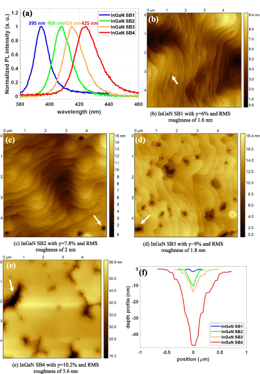
Figure 2. (a) PL of the InGaN SB templates, (b)–(e) 5 × 5 µm2 AFM data for InGaN SB1 to InGaN SB4, (f) depth profile of the V-pits labeled by the arrows in each of the four InGaN templates.
Download figure:
Standard image High-resolution imagePL results for MQW1 to MQW4 (grown on GaN) versus SBMQW1 to SBMQW4 (grown on Iny Ga1-y N SB templates) are shown in figure 3. A red shift in the QWs emission by 12, 31, 35, and 43 nm is observed when the underlying GaN is replaced with an InGaN SB template. The higher the In-content 'y' in the template, the larger the observed red shift. Data from this figure combined with modeling will be used to deduce the red shift and the enhancement of In-content in the QW due to their growth on the InGaN templates.
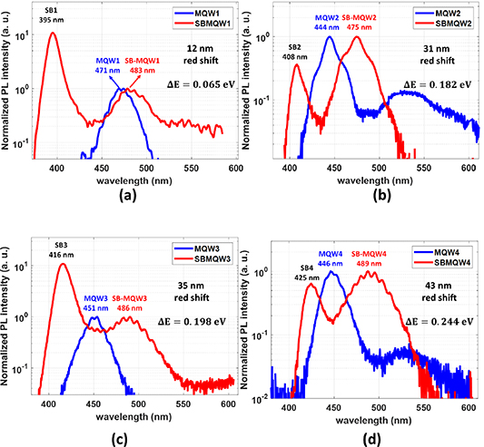
Figure 3. PL of MQWs grown on GaN (MQW1–MQW4) and on an SB template (SBMQW1–SBMQW4). The red shift increases with increasing In-content in the underlying SB template.
Download figure:
Standard image High-resolution imageTo understand the origin of this shift, several factors have to be taken into account that can affect the MQWs emission wavelength due to the presence of the underlying SB template. The reduction in strain in the MQWs as a result of the relaxed underlying template can affect three parameters: (a) band gap of InGaN QWs and GaN barriers, (b) induced piezoelectric field, and (c) increased indium incorporation in the QWs from x to z due to composition pulling.
A theoretical model was developed to investigate the effect of these parameters on the emission wavelength. The model first determines the strain in the wells and barriers from the mismatch between the QWs and the underlying template. This strain is then used to calculate the well/barrier band gaps and induced electric fields. The electric fields and band gaps are then used to construct Schrodinger's equation which is solved numerically to determine the energy states and wave functions in the wells.
The band gap of compressively strained Inx Ga1-x N, Eg InGaN(x), can be expressed as [15, 16]:
The effect of the polarization charges on emission is handled latter via the solution of the Schrodinger equation. The band gap of tensile strained GaN, Eg StrainedGaN, can be expressed as [17]:

where Eg
InN= 0.7 eV and Eg
GaN = 3.4 eV, the band gap bowing parameter is  [15], and
  is the strain in the basal plain. The electric field in the MQW structure is caused by the presence of spontaneous polarization (Psp) and strain induced piezoelectric polarization (PPZ). The total field in each of the QW and the barrier can be expressed as [18]:
where Pj/k
is the total polarization (sum of Psp and PPZ),  j/k
is the dielectric constant, and lk
is the thickness of each layer, k is an index that runs over the alternating InGaN wells and GaN barriers. The piezoelectric polarization can be calculated from [19, 20]:
j/k
is the dielectric constant, and lk
is the thickness of each layer, k is an index that runs over the alternating InGaN wells and GaN barriers. The piezoelectric polarization can be calculated from [19, 20]:

where  and
and  are the piezoelectric constants,
  is the strain in the basal plane,
  is the strain in the axial plane which can be calculated from
  using
using 
 , where Cij
are the material elastic constants [21].
, where Cij
are the material elastic constants [21].
The calculated band gaps and electric fields are then used to construct Schrodinger's equation for electrons and holes to determine the energy states and the electron/hole wave functions inside the QWs. A finite difference model was used to solve Schrodinger's equation using a similar scheme to Tan et al [22]. The parameters for GaN and InN used in the model and for the electric field calculations are from [20, 23]. Parameters for InGaN were calculated using Vegard's law with GaN and InN parameters. The band offset parameters for Inx Ga1-x N/GaN MQWs used in the model are the ones reported by Tsai and Bayram [24].
The model's additional inputs are the indium content, y, in the underlying SB template and its degree of relaxation, the well and barrier thicknesses, and the QWs emission wavelength from PL. The model then uses these inputs to predict the In-content, z, in the QWs grown on Iny Ga1-y N SB templates.
To validate the results of the model, high-resolution XRD (HRXRD) (0002) scans for MQW3 and MQW4 were used to estimate the In-content, x, in the QWs by using the PANalytical X'Pert epitaxy software as shown in figure 4. The HRXRD results were compared to the results obtained from the model. Table 1 lists the parameters of MQW structures, showing good agreement between the indium content, x, obtained from HRXRD and from the model for the two samples grown on GaN. For the SBMQW, it should be mentioned that HRXRD used to determine x in the QWs grown on GaN, was not successful to determine z for the QWs grown on the templates because of the satellite peaks due the periodicity in the InGaN SB templates.
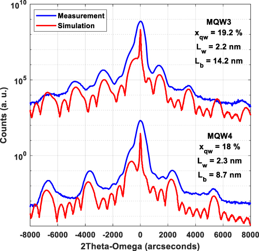
Figure 4. HRXRD (0002) scan of MQW3 and MQW4 versus simulation results showing the well and barrier thicknesses and the estimated In-content in the wells (xqw).
Download figure:
Standard image High-resolution imageTable 1. A summary of the In-content values obtained from the model versus HRXRD.
| MQW PL (nm) | No. of wells | Well width,  (nm) (nm) | Barrier width,  (nm) (nm) | In-content in QWs (x) from HRXRD | In-content in QWs (x) from model | |
|---|---|---|---|---|---|---|
| MQW3 | 451 | 3 | 2.2 | 14.2 | 19.2% | 19.36% |
| MQW4 | 446 | 5 | 2.3 | 8.7 | 18% | 18.7% |
The model was then applied on the PL data of MQW2 and SBMQW2. The indium content in MQW2 was estimated using the model to be x= 13.2%. For SBMQW2, the indium content in the SB was set to y= 7.8% and a degree of relaxation R= 75% as determined from TEM and EDS [10]. For the QWs in SBMQW2 structure, the indium content, z, is expected to be higher than 13.2% as a result of the composition pulling accompanied with the reduced strain. This has been previously reported for bulk InGaN films [1, 25–27] and we have previously reported it for InGaN SB [10, 11]. Recent reports on composition pulling in QWs due to strain reduction has also been reported [8, 28].
The exact In-content in the QWs of the SBMQW structure is proven to be challenging to determine experimentally. HRXRD is dominated by the periodicity of the InGaN template rather than the QWs and SIMS measurement performed on SBMQW2 showed an indium content of z ∼ 10% in the QWs which does not match the observed 475 nm emission from PL. InGaN SB templates increase the surface roughness which can degrade the depth resolution of SIMS leading to an underestimation of indium content [29].
Therefore, the model was used to estimate the increase in indium content that resulted in the observed 31 nm red shift in PL peak emission. The simulated band diagram for MQW2 is shown in figure 5(a) showing that an indium content of 13.2% results in the observed 444 nm PL peak emission. Figure 5(b) shows the simulated band diagram for the QW in the SBMQW2 structure, the In-content increases to z = 15.9% to result in the observed 475 nm emission. This represents a 20.45% enhancement in the In-content of the QWs due to the replacement of the GaN template with the InGaN SB template.
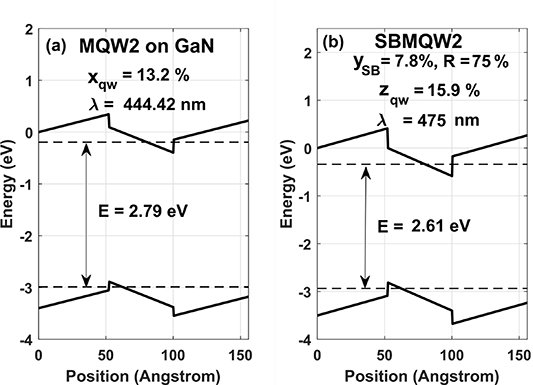
Figure 5. Simulated band diagram of MQW2 and SBMQW2 showing an increase in In-content from 13.2% for MQW2 to 15.9% for SBMQW2.
Download figure:
Standard image High-resolution imageIt should be mentioned from figure 5 that although the polarization charges of the well are expected to decrease because of the reduced strain, the enhancement in indium incorporation counters this effect along with the added polarization charge to the barrier that is now under tensile strain. Those two effects result in a comparable electric field in the well for both MQW1 and SBMQW1.
The model was then applied to the three other pairs in figure 3 to determine the dependence of the enhancement in indium incorporation on the indium content of the template.
A summary of the model results is presented in table 2. A relative increase in the QWs indium content by 6.28%, 20.45%, 25%, and 29.94% is estimated for SBMQW1, SBMQW2, SBMQW3, and SBMQW4, respectively.
Table 2. A summary of the four test pairs of MQWs grown on GaN and then repeated on an InGaN SB template.
| SB PL (nm) | MQW PL (nm) | Red shift (nm) | In-content in the template, y, and degree of relaxation, R | In-content in QWs from model | QW relative increase in In-content, 
| |
|---|---|---|---|---|---|---|
| MQW1 | — | 471 | — | y = 0% | x = 20.7% | — |
| SBMQW1 | 395 | 483 | 12 | y = 6%, R = 55% | z = 22% | 6.28% |
| MQW2 | — | 444 | — | y = 0% | x = 13.2% | — |
| SBMQW2 | 408 | 475 | 31 | y = 7.8%, R = 75% | z = 15.9% | 20.45% |
| MQW3 | — | 451 | — | y = 0% | x = 19.36% | — |
| SBMQW3 | 416 | 486 | 35 | y = 9%, R = 80% | z = 24.2% | 25% |
| MQW4 | — | 446 | — | y = 0% | x = 18.7% | — |
| SBMQW4 | 425 | 489 | 35 | y = 10.23%, R = 85% | z = 24.3% | 29.94% |
Figure 6 summarizes the change in the energy of the emitted photon as a result of replacing the underlying GaN layer with an InGaN template. Two points were added which were obtained from EL measurements rather than PL from fabricated LED devices, as indicated by a red x. The EL measurements were recorded at the minimum detectable injection current to minimize the effect of carrier screening on the emission wavelength. The results in figure 6 can be projected to show that an InGaN template with an indium content y ∼ 15% can be used to convert a blue LED grown on GaN to emit in the red spectrum. To account for the different degrees of relaxation in the templates, we define an effective In-content (yeff) which is the equivalent In-content if the film is fully relaxed. For example, the lattice constant of a template with y = 10% that is 85% relaxed is equivalent to a fully relaxed template with yeff = 8.5% using Vegard's law.
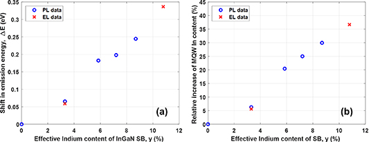
Figure 6. (a) Red shift in emission energy ( ) of MQWs versus the effective indium content in the SB templates, (b) relative increase in the indium content of MQWs versus the indium content in the SB templates.
Download figure:
Standard image High-resolution imageTwo pairs of LED devices were fabricated using similar structures of MQW (LEDGaN1 and LEDGaN2) and SB-MQW (LEDSB1 and LEDSB2), with the addition of a Mg-doped p-GaN cap layer. The LEDs' performance are used to investigate the impact of the templates on the device quality. The EL results are shown in figures 7(a) and (b). For LEDSB1, the InGaN templates is emitting at ∼395 nm, identical to SB1, while SB4 is emitting at 435 nm corresponding to an In-content of yeff= 10.8%. For the lowest injection current, figure 7(a) shows a 12 nm red shift between LEDGaN1 and LEDSB1 while figure 7(b) shows a 62 nm red shift. A shoulder peak is also observed at ∼550 nm for LEDSB2 which is suspected to be attributed to yellow luminescence deep level in GaN, as it has also been observed in the conventional MQW device [30]. The low In-content of the InGaN template in LEDSB1 does not deteriorate the optical output power of the device as shown in figure 7(c). This agrees with the expected surface morphology of the template as shown in the AFM data in figure 2(b). However, the (IV) measurements in figure 7(d) shows higher leakage current for LEDSB1 as compared to LEDGaN1 which can be attributed to the mismatch between the p-GaN cap and the InGaN template. For LEDSB2, the higher In-content of yeff = 10.8% results in a weaker output power and a higher leakage current. This deterioration in performance can be attributed to the increased surface roughness of the templates as SB4 has a surface roughness of ∼5 nm, shown in figure 2(e), also the lattice mismatch between the p-GaN layer and the relaxed InGaN template can lead to formation of new defects. The replacement of p-GaN layer with a lattice matched p-InGaN is currently being investigated to alleviate this issue. LEDSB2 was used to investigate the effect of an InGaN SB template with y ∼ 10% on the emission wavelength. Further investigation is still required to achieve InGaN templates with y > 10% with atomically smooth surfaces for optimized optical and electrical performance.

Figure 7. Comparison of EL of (a) conventional MQW on GaN device (LEDGaN1) versus SBMQW device (LEDSB1) grown on SB1. (b) Conventional MQW on GaN device (LEDGaN2) versus SBMQW device (LEDSB2). (c) Optical output power of LEDGaN1 versus LEDSB1. (d) IV measurements for LEDGaN1 versus LEDSB1.
Download figure:
Standard image High-resolution image
4. Conclusions
In conclusion, an investigation of the effect of Iny
Ga1-y
N SB templates on MQW emission, compared to those grown on GaN, has been presented. Theoretical modeling along with PL measurements show that a highly relaxed SB template with indium content ∼10% can cause a red shift up to ΔE ∼ 0.33 eV ( ) in emission. This red shift is due to the decreased strain in the QWs that results in a smaller band gap and an increase in indium incorporation due to the composition pulling effect. The presented model can be used to estimate the In-content and the enhancement in In-incorporation in the QWs for a given InGaN template from the red shift in wavelength measured by PL. These data can be used as a guideline to crystal growers in predicting the In-content in both the QWs and the templates to achieve the maximum red shift in a given LED structure. We are not aware of any similar modeling activities that take into consideration the changes in both indium content in the SB and QW due to the changes in the degree of relaxation. LED devices were fabricated using the proposed test structures showing a red shift in emission that agrees with what has been observed in PL and with comparable performance.
Acknowledgments
We would like to acknowledge the technical discussions with Dr N A El-Masry, Dr P Colter, and Nate Brown. This work is supported by National Science Foundation Grant Nos. ECCS-1407772, ECCS-1665211 and ECCS-1833323. This work was performed in part of the Analytical Instrumentation Facility (AIF) at North Carolina State University, which is supported by the State of North Carolina and the National Science Foundation (Award No. ECCS-2025064). The AIF is a member of the North Carolina Research Triangle Nanotechnology Network (RTNN), a site in the National Nanotechnology Coordinated Infrastructure (NNCI).