
Abstract
We propose a novel model approach for temperature evaluation in the channel region of a InAlN/AlN/gallium nitride high electron mobility transistor (HEMT) due to self-heating effects. The heat transfer in a HEMT device has been investigated experimentally by the nearby temperature sensor and compared by theoretical models solved by both numerical and analytical methods. The average temperature of the channel area of almost 160 °C for dissipated power of 2 W was determined using the drain-source current variation analysis. The electrical and thermal behavioral numerical model under quasi-static conditions have been used to describe the HEMT device. In contrast, the one-dimensional thermal model for analytical evaluation has been proposed as an alternative approach. Surprisingly, the experimental results verified not only the validity of precise numerical simulation but also the simplified analytical model that makes it a reliable tool even for complex electronic devices.
Export citation and abstract BibTeX RIS

Original content from this work may be used under the terms of the Creative Commons Attribution 4.0 license. Any further distribution of this work must maintain attribution to the author(s) and the title of the work, journal citation and DOI.
1. Introduction
The Internet of Things represents the coming technical revolution that will hit all areas of human society. The rising era of sensors, smart cities, and e-health results in an incredible load of wireless networks. Furthermore, the recent development of augmented reality, autonomous cars, and high-resolution video streaming creates a need for high-speed transmission, large bandwidth, or high capacity of the network. These requirements are beyond the capabilities of the present mobile network; hence, as a response, the fifth-generation (5G) mobile network has been envisioned as the next big thing that will change the world of data transmission. It should be mentioned here that the 5G network represents a broad interdisciplinary challenge that also requires advanced electronic devices and systems. The performance of a radio-frequency power amplifier dominates the overall transmitter performance. Imperfect amplifiers define the power and heat dissipation for the entire system. Even though silicon (Si) dominates in the area of consumer electronics, the III–V semiconductors are often proposed because of their superior frequency responses, high-temperature tolerance, or breakdown robustness. Among them, gallium nitride (GaN) is recognized as the most promising candidate for high-power and high-frequency devices since we are capable to fabricate a heterostructure that exhibits a presence of two-dimensional electron gas (2DEG). This outstanding nature gives us the potential to create high electron mobility transistors (HEMTs), which have emerged as excellent devices for applications in the power conversion field. However, the high mobility combined with a high density of the electrons in 2DEG leads to the possibility of the device self-heating due to Joule losses. The rise of temperature influences the device's electrical properties as well as entire system performance and reliability [1–3]. Suppressing the negative impact of the elevated temperature substrates with high thermal conductance has been proposed. Hence, advanced power devices are grown on advanced substrates, e.g. silicon carbide (SiC) and Si exhibit better power dissipation in comparison to the conventional sapphire substrates [4]. However, even though high-cost substrates are applied, self-heating remains a crucial issue for these devices. Since the HEMT devices are microscopic in size, temperature study by conventional methods is not possible. Therefore, the temperature distribution in HEMT devices represents now the gap in the knowledge, and enormous effort has been put into the development of novel experimental techniques that can provide an insight into the heat dissipation. Optical methods such as Raman spectroscopy or interferometric mapping are widely applied since they offer a low-cost and contactless tool for accurate measurements [5–7]. However, the temperature evaluation often requires support from device simulation because it represents indirect measurement methods. The analytical approach that can compete with numerical methods remains a great challenge for such a complex system.
This work demonstrates the application of selected theoretical models for heat dissipation for temperature evaluation in the channel region of a InAlN/AlN/GaN HEMT device. The analytical approach is compared with the numerical simulation and experimental observation of the temperature distribution. An electrical and thermal behavioral model under quasi-static conditions is used to describe the HEMT device [8]. The average temperature of the active device area is evaluated and compared with the experimentally determined one.
2. Experimental
2.1. Structure design and experimental setup
The investigated In0.185Al0.815N/AlN/GaN HEMT structure including 6.3 nm In0.185Al0.815N/1.5 nm AlN/1830 nm GaN heterostructure was grown by MOVPE on 350 μm thick 4 H-SiC substrate. The backside Au contact is soldered to 1 mm thick CuMo leadframe by 60 μm thick AuSn solder. Top ohmic drain/source and gate contacts were created by standard Au-based metallization.
Gated transmission line model (GTLM) HEMT of width w ≈ 100 μm with a gate of length dG ≈ 0.15 μm situated in the middle of the source to drain gap of length dSD ≈ 2.5 μm was investigated. As a temperature sensor, a parallel TLM structure of length dTLM ≈ 2.5 μm and width w ≈ 100 μm located in the distance of dGT ≈ 120 μm from GTLM HEMT was utilized as shown in figure 1. The device is set in the open package placed on the Al thermal chuck preserved at a constant temperature.
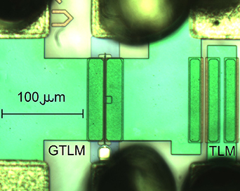
Figure 1. Horizontal view and position of GTLM HEMT and TLM structure.
Download figure:
Standard image High-resolution imageSemiconductor parameter analyzer Agilent 4155C and controlled thermal chuck were utilized to acquire output characteristics at zero gate-source voltage VGS and drain-source voltage VDS varied from 0 V up to 20 V together with average TLM temperature TS obtained as the current temperature dependence at constant voltage ∼0.5 V in the low-power operating regime. The chuck temperature was set in the range 25 °C–85 °C to demonstrate and to compare methods based on ambient temperature and dissipated power variation. The device was recovered by white LED illumination for 1 min between measurements. The three-dimensional (3D) thermal FEM simulations of the device were performed by Synopsys TCAD Sentaurus [8, 9]. The 3D model was created according to device geometry, layout and thickness of individual layers. Material thermal conductivity values were obtained from the previous work and calibrated utilizing the measurements [10]. The boundary condition of the constant ambient temperature is set to the structure backside based on ideal heat transfer to the heatsink. The structure self-heating is simulated by three thermal contacts placed along 2DEG between drain and source. The individual heat sources represent heat contribution from drain to source the access region, the region under the gate electrode and the pinch-off region located at the drain side gate edge [11].
2.2. Average channel temperature determination
The drain–source current IDS dependence on the drain–source voltage VDS for gate–source voltage VGS = 0 V at varying ambient temperature T0 in the range of 25 °C–85 °C and sensor temperature TS dependence on total dissipated power P were acquired as shown in figures 2 and 3, respectively. Low temperature-dependent threshold voltage VTH ≈ −3.8 V acquired from semi-logarithmic transfer characteristics of the transistor, VGS = 0 V and drain to gate voltage drop VDG ≈ 1.5 V allows us to estimate saturation voltage  corresponding to the measured value VDS,SAT ≈ 6 V.
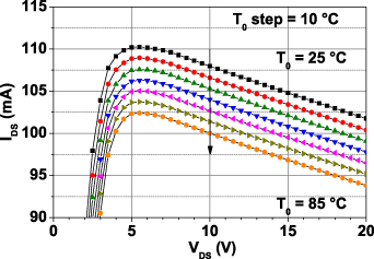
Figure 2. Output characteristics for gate-source voltage VGS = 0 V at various ambient temperatures T0.
Download figure:
Standard image High-resolution image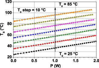
Figure 3. Sensor temperature TS dependence on dissipated power P at various ambient temperatures T0.
Download figure:
Standard image High-resolution imageThe electro-thermal model offers an approximate pinch-off area length increase under the gate dPO/VPO ≈ 0.4 nm V−1 and gate to drain area dPD/VPO ≈ 2.2 nm V−1 utilizing pinch-off voltage VPO in the saturation regime. 3D thermal FEM simulations are keeping up with HEMT dimensions such as dPO and dPD. Assuming  the channel length modulation caused by dPO results in the constant ratio
  [8]. Small dG brings notable gD in comparison with measured output conductance dIDS/dVDS including self-heating. Various methods are advisable to compare and obtain proper gD value having a significant impact on average channel temperature TA determination for short gated HEMT.
Differential thermal resistance RA(T0) vs. P and RA(T0) vs. T0 at different T0 calculated by equation (11) (see appendix) is shown in figures 4 and 5, respectively. The increase of RA with P at defined T0 is partially caused by spatially distributed electrical parameters of the active device area such as gD variation which is caused mainly by non-linear pinch-off length dependence on VDS insufficiently described in the electro-thermal model. Therefore, RA approximate value at defined T0 is depicted in figure 5.
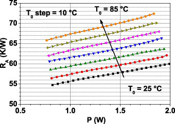
Figure 4. Thermal resistance RA dependence on dissipated power P at various ambient temperatures T0 utilizing equation (11) in the appendix.
Download figure:
Standard image High-resolution image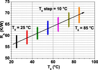
Figure 5. Thermal resistance RA dependence on average temperature TA equal to the ambient temperature T0.
Download figure:
Standard image High-resolution imageDirectly acquired  from sensor temperature TS dependence on power dissipation P and RS00 calculated by equations (11) and (22) (see appendix) are similar due to the negligible influence of dissipated power spatial distribution in linear and saturation regime on the far location of the sensing element despite TLM width. To include the device topology the distance s/l ratio is defined where s is the distance of the sensor device (TLM), and l is the channel distance (GTLM) from the surrounding area with the ambient temperature. In other words, s/l close to one represents sensor device nearby the channel region, whereas s/l ratio approaching zero stands for sensor device far away from the channel region. Utilizing equations (14) and (22) and assuming aM ≈ 1 dissipated power variation method allows us to plot s/l(TS) vs. P, RA(TS) vs. P and RA(TS) vs. TS dependence at different T0 as shown in figures 6–8, respectively. The dissipated power variation method based on TS acquisition across the whole TA range requires much higher VDS as well as gD range than the ambient temperature variation method. Therefore, RA and s/l deviation are more significant especially for RA being slightly dependent on TA. Measured data approximation eliminates missing overlap of RA(TS) vs. TS for different T0 caused by gD
variation and spatially distributed electrical parameters as shown in figure 8.
from sensor temperature TS dependence on power dissipation P and RS00 calculated by equations (11) and (22) (see appendix) are similar due to the negligible influence of dissipated power spatial distribution in linear and saturation regime on the far location of the sensing element despite TLM width. To include the device topology the distance s/l ratio is defined where s is the distance of the sensor device (TLM), and l is the channel distance (GTLM) from the surrounding area with the ambient temperature. In other words, s/l close to one represents sensor device nearby the channel region, whereas s/l ratio approaching zero stands for sensor device far away from the channel region. Utilizing equations (14) and (22) and assuming aM ≈ 1 dissipated power variation method allows us to plot s/l(TS) vs. P, RA(TS) vs. P and RA(TS) vs. TS dependence at different T0 as shown in figures 6–8, respectively. The dissipated power variation method based on TS acquisition across the whole TA range requires much higher VDS as well as gD range than the ambient temperature variation method. Therefore, RA and s/l deviation are more significant especially for RA being slightly dependent on TA. Measured data approximation eliminates missing overlap of RA(TS) vs. TS for different T0 caused by gD
variation and spatially distributed electrical parameters as shown in figure 8.
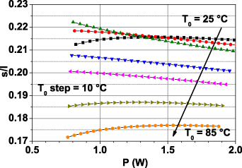
Figure 6. The s/l ratio dependence on dissipated power P at various T0 utilizing equation (14) in the appendix.
Download figure:
Standard image High-resolution image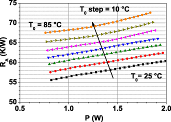
Figure 7. Thermal resistance RA dependence on dissipated power P at various ambient temperature T0 utilizing equation (15) in the appendix.
Download figure:
Standard image High-resolution image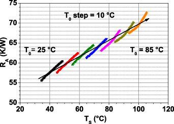
Figure 8. Thermal resistance RA dependence on average temperature TA equal to the sensor temperature TS.
Download figure:
Standard image High-resolution imageApproximate thermal resistance RA dependence on ambient temperature T0 and sensor temperature TS, respectively, depicted in figures 5 and 8 with consecutive linear fit gives us the opportunity to plot average temperature TA dependence on dissipated power P depicted in figure 9 utilizing equations (13) and (16) (see appendix). For constant VGS applied to the InAlN/AlN/GaN HEMT self-heating results in IDS decrease caused mainly by thermally induced serial source area resistance increase [8]. Therefore, the average temperature of the source to the gate area is related to TA. Simulated and calculated results are in good agreement as depicted in figure 9.

Figure 9. Average temperature TA vs. dissipated power P dependence acquired by ambient temperature T0 and sensor temperature TS variation.
Download figure:
Standard image High-resolution image3D thermal FEM simulations were utilized to acquire HEMT channel temperature TC vs. distance xs from the drain side of the gate edge perpendicular to the gate in the middle of the HEMT width as shown in figure 10. Due to different dissipated power spatial distribution in the pinch-off area and source to drain region, the condition  needed for low VDS is gradually turned into
  for high VOUT; these conditions are required for regular s/l determination.
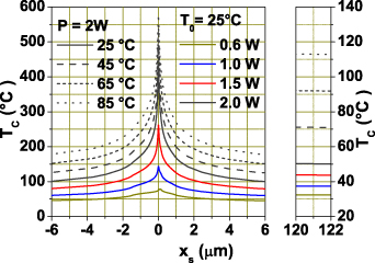
Figure 10. Spatial distribution of channel temperature TC for various dissipated power P.
Download figure:
Standard image High-resolution imageThese conditions also allow acquisition of xs and TC vs. s/l ratio dependencies for different dissipated power P at T0 = 25 °C utilizing equations (23) and (24) (see appendix) and the quadratic fit of simulated average temperature TA vs. P dependence, as shown in figure 11. Fulfilled condition  results in xs vs. s/l ratio plot independent of dissipated power.

Figure 11. Channel temperature TC and s/l ratio profile for various dissipated power P at ambient temperature T0 = 25 °C.
Download figure:
Standard image High-resolution imageThe procedure mentioned above applied for P = 2 W at different T0 makes it possible to obtain xs and TC vs. s/l ratio dependencies as depicted in figure 12. Condition  fulfilled for P = 2 W is assumed as well as for lower dissipated power resulting in aM ≈ 1 across the operating range.
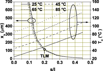
Figure 12. Channel temperature TC and s/l ratio profile for P = 2 W at various ambient temperatures T0.
Download figure:
Standard image High-resolution image3. Conclusions
The temperature sensor placed nearby the active device area was employed in order to minimize ambient temperature variation across the whole operating temperature range. The experimental part deals with an average InAlN/AlN/GaN HEMT channel temperature determination utilizing electrical parameters acquired by quasi-static measurements. Subsequently, the electrical and thermal models were analyzed to determine the average temperature of the active device area using ambient temperature and dissipated power variation methods under quasi-static conditions.
Average channel temperature TA ≈ 160 °C indicating the major change of thermal resistance RS calculated for dissipated power P = 2 W in GTLM InAlN/AlN/GaN HEMT structure shows a good agreement with simulated results. Robust 3D thermal numerical simulations were a stimulus to develop a simplified analytical model.
Proper isothermal output conductance acquisition makes this method applicable for a field-effect transistor (FET), TLM structure or Schottky diode. Average channel temperature TA is related to the most thermally sensitive element of the device, TA evaluated by the proposed one-dimensional analytical model is close to the average temperature of the source to drain area of investigated HEMT determined by numerical simulations. The different influence of dissipated power and ambient temperature variation on heat flux distribution across the temperature sensor is negligible if the sensor is located far from the active area in comparison with a source to drain distance. The suggested analytical model represents a reliable and straightforward alternative for numerical simulations of complex HEMT devices.
Acknowledgments
The research leading to these results has received funding from the ECSEL Joint Undertaking (JU) under Grant Agreement No. 783274. The JU receives support from the European Union's Horizon 2020 research and innovation programme and France, Germany, Slovakia, Netherlands, Sweden, Italy, Luxembourg, Ireland. This publication reflects only the author's view and the JU is not responsible for any use that may be made of the information it contains. The work was also supported by Grant VEGA 1/0733/20 through the Ministry of Education, Science, Research and Sport of Slovakia.
Appendix.: Theory
Appendix. Thermal model
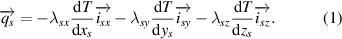
In general under the quasi-static operating condition and dissipated power free space heat transfer equation describes heat flux vector  dependent on temperature gradient T and thermal conductivity
  in 3D orthogonal space using cartesian vectors
  ,
,  ,
,  and coordinates
  [12]:
[12]:
Heat flux from device active area to defined ambient temperature T0 boundary forms equithermal surface consisting of elementary surfaces  utilizing perpendicular
  vector. Equithermal elementary surfaces shifted by
  exhibit dT in
  direction and equation (1) result in
  which is possible to be integrated across the equithermal surface utilizing spatially dependent
  and λl
:
and λl
:
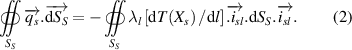
The left side of equation (2) represents total dissipated power P of the active area for all power sources situated inside the space bounded by equithermal surface. The right side of equation (2) results in scalar form and makes transformation of 3D heat propagation into 1D possible by application ![$\mathop{\unicode{x222F}}\limits_{{S_S}} {{\lambda _l}\left[ {{\text{d}}T\left( {{X_s}} \right)/{\text{d}}l} \right].{\text{d}}{S_S}} = {\lambda _{\text{T}}}\left( T \right)S{\text{d}}T\left( x \right)/{\text{d}}x$](https://content.cld.iop.org/journals/0268-1242/36/2/025019/revision3/sstabd15aieqn21.gif) utilizing position x of equithermal surface in the space of constant area S, constant heat flux
utilizing position x of equithermal surface in the space of constant area S, constant heat flux  and scalar thermal conductivity λT as shown in figure 13. This reduces equation (2) into 1D equation (9):

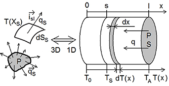
Figure 13. 3D to 1D thermal model transformation.
Download figure:
Standard image High-resolution imageConstant heat flux q evenly produced at  results in temperature profile T(x) assuming zero λT for
  and
and  set at zero x. Thermal resistance
  utilized in equation (3) for
  is temperature-dependent only.
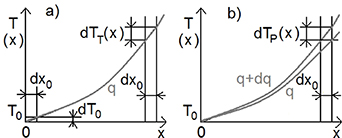
If a block of fixed length and heatflux is prolonged by dx0
then  using
using  and subsequently
  as shown in figure 14(a). Length shift dx0
here is possible to be caused by ambient temperature shift dT0
and the ratio between dTT(x) and dT(0) dTT(x) is determined:
as shown in figure 14(a). Length shift dx0
here is possible to be caused by ambient temperature shift dT0
and the ratio between dTT(x) and dT(0) dTT(x) is determined:

Figure 14. 1D thermal model for (a) dT0 and (b) dq.
Download figure:
Standard image High-resolution image
Two different heat flux intensities qA, qB
with corresponding length differences dxA
, dxB
result in similar temperature difference  for the same temperature. Subsequent integration with boundaries 0, xA
and 0, xB
supposing
for the same temperature. Subsequent integration with boundaries 0, xA
and 0, xB
supposing  yields:

Heat flux increase  results in temperature increase
  for x < l as depicted in figure 14(b). Substitution
  ,
,  ,
,  ,
,  in equation (5) resulting in
  makes it possible to determine dTP(x):

Differential thermal resistance  brings
  . In similar way
  is defined, therefore equation (4) yields:

It is possible for  to be invoked by dissipated power increase dP produced at l. On the other hand at constant P ambient temperature increase, dT0
*
results in dT*
(x) consisting of
to be invoked by dissipated power increase dP produced at l. On the other hand at constant P ambient temperature increase, dT0
*
results in dT*
(x) consisting of ![${\text{d}}{T_{\text{T}}}\left( x \right) = \left[ {R\left( x \right){\text{/}}{R_0}\left( x \right)} \right]{\text{d}}T_0^*$](https://content.cld.iop.org/journals/0268-1242/36/2/025019/revision3/sstabd15aieqn44.gif) at constant dissipated power and
at constant dissipated power and  caused by dissipated power difference dP*
at constant T0.
caused by dissipated power difference dP*
at constant T0.
Subsequently subtitution  in
in  yields:
As depicted in figure 1 average temperature TA assumed as a constant value across the device active area defines the boundary conditions T(0) = T0 at x = 0 and T(l) = TA at x = l and dT* (l) = dTA * , dTT(l) = dTA T, dTP(l) = dTA P, R(l) = RA, R0(l) = RA0, k(l) = kA. Thermal parameters TS, dTS * , dTS T, dTS P, RS, RS0, kS of spot temperature sensor placed at x = s utilizing transformation shown in figure 1 are assigned in the similar way.
Various spatial power density contribution for dP and dP* has negligible influence on heat flux distribution relatively far from the active area. On the other hand, due to various temperature dependence of thermal conductivity a heat flux change across the structure caused by dP, dT0 * , dP* is unequal resulting in equithermal surface deformation causing x shift in 1D thermal model. In general, the ratio between l and s varies with P and T0.
Appendix. Average temperature active area electrical model
Active device at operating point characterized by output, namely drain–source voltage and drain–source current (VDS, IDS), input, namely gate-source voltage VGS and zero input, namely gate current at average active area temperature TA is inspected under quasi-static operating conditions. Output current difference dIDS is defined by device transconductance  and output conductance
  at constant TA and thermal coefficient
  determined at constant VGS and VDS [13]:

Coefficients gM, gD, kTH are determined from electrical parameters at operating point (VGS, VDS, TA) and are required to be independent of th entire device thermal parameters [14].
At constant VGS and VDS small ambient temperature increase dT0
*
results in dTA
*
inside the active area and current change dIDS
*
is supposed and dTA
* is also influenced by dissipated power variation  .
.
Increasing VDS at constant VGS results in dTA, caused by dVDS and dIDS and in dissipated power change  . Whereas equation (9) results in
  and
and  , consecutive substitution yields:

Rising VDS at constant VGS brings an increase of dissipated power mainly in the pinch-off area for field-effect transistor (FET in saturation regime, though dissipated power contribution in the entire active device area is evident especially for low VDS. The different mode of dP and dP*
influence on heat flux distribution across the spot temperature sensor is negligible for  or sensor location far from the active area in comparison with a source to drain distance. In the case of TLM structure the dP and dP*
spatial distribution plays a lesser role. In the case of Schottky diode or multi-fingered device, an appropriate location of the spot temperature sensor is coming out from the principles mentioned above.
or sensor location far from the active area in comparison with a source to drain distance. In the case of TLM structure the dP and dP*
spatial distribution plays a lesser role. In the case of Schottky diode or multi-fingered device, an appropriate location of the spot temperature sensor is coming out from the principles mentioned above.
Proper device simulations such as pulse measurements allow gD acquisition taking leakage paths, trapping and other secondary effects into account [15]. Correct TA determination is influenced by dissipated power produced by temperature sensor as well.
Appendix. Ambient temperature variation
Although this method has been introduced [16], the theoretical background and requirements are mentioned here. Utilizing equation (8) in the active area yields:
Coming out from equations (10) and (11) zero gD results in:

Variation of T0 across the assumed operating temperature range allows us to obtain  resulting in
  for TA ≈ T0. Recurrent calculations of TA are processed in this way:

In equation (13) T00 represents the starting ambient temperature whereas  is calculated using equation (11) at increased T0. This method requires accurate T0 determination across the whole TA range independent on dissipated power. Otherwise RA0 variation with changing VDS at defined TA ≈ T0 points on improper gD assumption or phenomena caused by spatially distributed electro-thermal parameters, temperature gradient and different allocation of dissipated power change dP and dP*
along the active device area.
is calculated using equation (11) at increased T0. This method requires accurate T0 determination across the whole TA range independent on dissipated power. Otherwise RA0 variation with changing VDS at defined TA ≈ T0 points on improper gD assumption or phenomena caused by spatially distributed electro-thermal parameters, temperature gradient and different allocation of dissipated power change dP and dP*
along the active device area.
Appendix. Dissipated power variation
This method is advisable to acquire average temperature TA if a small-sized temperature sensor is placed relatively far from an active device area because of the negligible influence of different dissipated power spatial distribution on sensor temperature TS. For FET and temperature sensor placed nearby the active device supposing  the TA deviation is expected due to different dissipated power spatial distribution in the pinch-off area and source to drain area playing a lesser role with increasing VDS.
The ratio  coming out from constant rT(x) at T0 ambient temperature and comparison of equation (11) applied for RA0 and RS0 yields:
Similarly the same temperature-dependent rT(x) at TS utilizing  applied for RA and
  results in:

Consecutive RA utilization for TS ≈ TA brings:

Results from equations (14)–(16) are applicable in a straight way for the structure consisting of materials exhibiting a constant ratio of particular thermal conductivities within the operating temperature range. In this case, spatial heat flux distribution left intact for dT0 * and evenly increased for dP and dP* results in unchanged equithermal surface shape corresponding to particular spatial position.
However, various thermal conductivity dependence on temperature requires us to be aware of s position shift caused by unequal heat flux change invoked by dT0
*
or dP and dP*
. For temperature sensor the difference between measured temperature shift dTSM, dTSM
*
and temperature shift dTS, dTS
*
mentioned above exhibit difference of  where dsT is caused by dT0 and dP results in dsP and dP*
proportionally in
where dsT is caused by dT0 and dP results in dsP and dP*
proportionally in  :
:


Measured thermal resistance  exhibits:

Substitution  and
and  in
in  brings:

For  the conditions
  and
and  result in
  ,
,  giving an opportunity to s0/l acquisition.
The shift ratio  is required to substitute
  in equations (14) and (21) due to different spatial heat flux redistribution caused by dT0
*
or dP and dP*
. Supposing thin top layers in comparison with a relatively thick substrate and conventional temperature sensor location nearby the active device area on the top of the structure, then
in equations (14) and (21) due to different spatial heat flux redistribution caused by dT0
*
or dP and dP*
. Supposing thin top layers in comparison with a relatively thick substrate and conventional temperature sensor location nearby the active device area on the top of the structure, then  assumption resulting in
  brings sufficient accuracy. Otherwise, the thermal model based on partial heat flux distribution is requisite. Substitution
  coming out from s/l ratio dependence on P utilized in equations (15), (17) and (19) allows RA calculation:
The starting operating point is commonly set at  for small P resulting in RS00 and s0/l. In the FET case, the initial operating point is shifted to the saturation voltage VDS,SAT with active area average temperature TA,SAT whereas relatively low gD for VDS > VDS,SAT exhibits minor impact on TA determination especially for long gated FET [12]. Initial s/l ratio at
  is calculated utilizing equation (14).
Dissipated power variation method requires TS to be swept across the whole TA range being aware of dissipated power limitation. The solution in equation (11) is consistent with equation (22) for s/l ratio close to zero; therefore, both methods mentioned above are allowed to be combined if measurement setup is limited by T0 or P operating conditions.
Appendix. Thermal model transformation
This part deals with s/l ratio acquisition if thermal parameters of the active device area and temperature sensor P, T0, TA, TS are obtained from simulations or spatial calculations. The equithermal surface of temperature TS and s/l ratio meets the requirements mentioned above. In a simple way equation (3) is able to be rewritten as:

At defined T0, the dissipated power PA needed for reaching TS in the active device area at l position is applied. Subsequently the dissipated power PS at l position needed for reaching TS nearby temperature sensor at s position is set. Substitution  and
and  in equation (5) yields:

The procedure mentioned above allows us to acquire TS dependence on s/l ratio for various P and T0 and subsequently calculate  and
and  for defined s/l. Utilizing thermal resistance
  ,
,  at defined s/l and
  ,
,  at a spatial position corresponding to s/l ratio allows us to verify them coming out from equations (17)–(19):


The shift ratio calculated as  brings correction of s/l ratio calculations equation (14) from experimental data.