
Abstract
Recently a novel photonic integration technology, based on a thin InP-based membrane, is emerging. This technology offers monolithic integration of active and passive functions in a sub-micron thick membrane. The enhanced optical confinement in the membrane results in ultracompact active and passive devices. The membrane also enables approaches to converge with electronics. It has shown high potential in breaking the speed, energy and density bottlenecks in conventional photonic integration technologies. This paper explains the concept of the InP membrane, discusses the versatility of various technology approaches and reviews the recent advancement in this field.
Export citation and abstract BibTeX RIS

Original content from this work may be used under the terms of the Creative Commons Attribution 4.0 license. Any further distribution of this work must maintain attribution to the author(s) and the title of the work, journal citation and DOI.
Corrections were made to this article on 17 March 2023. The citation year was amended.
1. Introduction
Since the first introduction in 1969 [1], photonic integrated circuits (PICs) have experienced significant developments over the past decades, driven first by telecommunication, then by datacommunication and sensing. The InP based PICs have achieved the highest level of maturity due to the advancement of semiconductor lasers and other active devices, as well as the capability for full active-passive system-on-chip integration [2]. A generic foundry model for InP PICs has been established to further reduce the entry cost of prototyping by researchers and small and medium enterprises [3]. This path is later on followed by other PIC material platforms.
The level of integration in InP PICs has followed a similar path to that of the Moore's law in electronic integrated circuits (ICs) [4], with a highest report integration complexity of nearly 2000 functions per chip for a multi-channel coherent transmitter reported in 2014 [5]. Empowered by such integration complexity, record 4.9 Tbps data capacity in a single chip has been demonstrated [6]. However, such an increase in complexity and data capacity comes at the price of larger chip area and higher cost. In fact the integration density per unit chip area has not been improved much over the past 10 years [7]. Further increase of the integration density may find fundamental difficulties coming from the current waveguide structures with low optical confinement.
Silicon photonics on the other hand promises high optical confinement in its sub-micron waveguides and a route to manufacturability, leveraging the complementary metal-oxide semiconductor (CMOS) process compatibility [8]. However, the key function, the on-chip amplification, still requires hybrid integration of III–V materials. III–V-on silicon integration methods include single device die bonding and post-processing [9, 10] and direct epitaxy with the assistance of thick buffer layers [11]. Both approaches show potential for wafer-scale III–V material coverage on silicon circuits. But the integration density, especially for the active gain components, remains at a similar level to that of the conventional InP PICs. This is because the layer stacks and structural dimensions of the hybrid III–V devices still follow the classical designs.
Realizing InP-based III–V integration in a sub-micron thin membrane, similar to the silicon on insulator (SOI) platform, is a promising approach to fundamentally break the density bottleneck in actives. The membrane structure ensures a high optical confinement in monolithic active and passive devices and opens new opportunities for novel active diode designs. Over the past decade, significant research milestones have been achieved in InP membrane photonics by several groups worldwide. The high design flexibility of the InP membrane has led to several membrane platforms with various different design and technology philosophies for different application purposes.
In this paper we review the research lines of the integrated membrane photonics based on InP, and its III–V ternary and quaternary material system. We aim to provide a comprehensive overview of the developments in this field. The paper is organized as follows. Section 2 discusses the two major design approaches for the InP membrane, namely the lateral diode and the vertical diode. The membrane technologies are discussed in section 3, with a focus on opportunities and challenges when processing the InP membrane. Sections 4–7 present recent demonstrations of active and passive devices. Section 8 reviews two approaches of photonic electronic co-integration for InP membranes. Section 9 showcases several applications in which the InP membrane circuits can have high potential. In section 10, we will give our conclusions.
2. Active-passive integration concepts in InP membrane
The design of the active structures on InP membrane requires a trade-off between the optical and electrical properties, especially on the thicknesses of the core and cladding layers. Thinner layers would bring in the benefits of higher optical confinement factor and lower diode resistance, while at the same time impose challenges in the management of the optical loss and the sheet resistance in thin conductive layers. Comparing to the conventional amplifiers, the design trade-off is more prominent in the InP membranes.
The most important feature of the membrane structure is having strong optical confinement as illustrated in figure 1. With the optimal thickness of the membrane film, the optical confinement factor of the semiconductor core layer can be three times higher than in the conventional amplifier structure with semiconductor cladding layers. To fully benefit from such strong optical confinement, the core layer thickness of the membrane structure must be thin, which give a challenge for electrical injection. Since the conventional structure has relatively thick cladding layers, the electrodes, which have very high optical absorption, can be introduced to the top and bottom of the diodes and current can be injected along the vertical direction. On the other hand, for the membrane structure, the electrodes cannot be put directly on the top or the bottom, since the cladding layers in the vertical direction are either air or insulator. Therefore, to inject current to the membrane structure, electrodes at the sides of active region are required. Although the current then initially flows in the lateral direction, the PIN junction can be either in the lateral or vertical direction.

Figure 1. Comparison of the optical confinement between the semiconductor laser and membrane laser.
Download figure:
Standard image High-resolution imageThis section and the next section explain the lateral and vertical injection schemes, respectively.
2.1. Lateral diode scheme
Figure 2(a) shows the basic structure of lateral current injection (LCI) type membrane lasers [12–14]. The LCI structure itself was proposed by Oe et al [15] for the purpose of photonics–electronics integration before the membrane structure was proposed. One side of the active region has p-type layers and the other has n-type layers. A buried hetero (BH) structure should be introduced by regrowth technology to realize good current confinement as well as refractive index difference for lateral optical confinement. Recently, Aihara et al have reported BH fabrication by direct wafer bonding of an active stack to silicon, followed by regrowth steps to form the passive and doped regions [16]. To make the p- and n-type layers as side cladding layers, there are two methods. One is two times selective regrowth of p- and n-layers, once for each side [17]. The other way is one uniform regrowth of undoped layers, then applying impurity diffusion or implantation to form the p- and n-doped regions [16, 18]. The advantage of this LCI structure for the membrane structure is the relatively simple fabrication process (even though the regrowth is needed). After wafer bonding on a host substrate, the fabrication process basically continues as a planar process. The details are discussed in section 3. As a potential challenge, we have to care about the quality of the regrowth interfaces between side cladding layers and active region. This interface may affect the electrical characteristics (e.g. an excess voltage drop) and the optical characteristics induced by surface recombination. To avoid this, a carefully considered regrowth process, especially regarding the preparation process, is important.

Figure 2. (a) Basic structure of LCI-type membrane lasers. (b) Optical confinement factor of membrane structure [19]. (c) Internal quantum efficiency of Fabry–Perot membrane lasers as a function of InP cap layer thickness. (d) Cavity length dependence of external differential quantum efficiency of Fabry–Perot membrane lasers [20].
Download figure:
Standard image High-resolution imageAs shown in figure 2(a), the total layer thickness is as low as several 100 nm. Even with such a small thickness, careful consideration of the layer structure is very important to achieve high performance characteristics. Figure 2(b) shows the optical confinement factor as a function of the core thickness. It reaches maximum at the thickness of 150 nm. However, with considerations of high-speed modulation characteristics and current injection efficiency, the thickness of 150 nm may not be enough because of two reasons. The first of these is about surface recombination. Active layers (quantum wells (QWs) and barriers) usually consist of GaInAsP/GaInAsP or AlGaInAs/AlGaInAs for 1.3 µm or 1.55 µm lasers. Such material with As atoms tend to have a high surface recombination rate, which create non-radiative recombination carriers [21, 22]. Figure 2(c) shows the internal quantum efficiencies of Fabry–Perot membrane lasers as a function of InP cap layer thickness at the surface. We can see clear improvement of the internal quantum efficiency by increasing the cap thickness up to 50 nm. Therefore, these active layers should be sandwiched by sufficiently thick layer of InP, which is the material with low surface recombination rate. Second, multiple QWs should be used to increase the differential gain, for high speed operation. Therefore, the total thickness becomes >200 nm.
Next, the structure in the lateral direction is discussed. Since the membrane structure has a small layer thickness, the electrical resistance tends to be high. Also, optical absorption can be high because of the strong interaction with lossy materials. Therefore, a balance between electrical resistance and optical absorption is a key design point. Figure 2(d) shows the cavity length dependence of external differential quantum efficiency of Fabry–Perot membrane lasers with two different p-type doping concentrations in the InP cladding layer. Clear difference of the internal loss can be seen between the two structures. Therefore, the final design uses a p-type doping concentration of 5 × 1017 cm−3 and a 2 µm distance between the edge of an electrode and the active region [20].
After consideration of the design of the cross-section, the cavity structure also should be considered for lasers. Three different cavity structures, namely distributed feedback (DFB), distributed reflector (DR) and photonic crystal (PhC), are briefly introduced in the next sections.
2.1.1. DFB and DR structures.
A DFB structure is commonly used in conventional laser structures for single mode and low threshold current operation. The concept is also applicable to the membrane lasers. Furthermore, by introducing an additional distributed Bragg reflector at the rear side of the membrane DFB lasers, a higher output efficiency can be realized at the front side. This structure is so called a DR structure [23–25]. The typical structure of DR lasers is shown in figure 3. A surface corrugation grating is introduced to achieve a high coupling coefficient κ of >1800 cm−1 for a short cavity length. The output passive waveguides are integrated by butt-coupling, using crystal regrowth, similar to the BH structure mentioned above [17]. Although a coupling coefficient κ as high as ∼4000 cm−1 can be realized with a deep grating depth, such high coupling coefficients give low output power. Therefore, the choice of κ depends on the requirements for each application. The details of design and characteristics of DR lasers are explained in section 4.2.
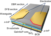
Figure 3. GaInAsP DR membrane lasers [23].
Download figure:
Standard image High-resolution image2.1.2. PhC structure
To realize ultra-low threshold current operation such as <10 µA, an introduction of PhC is effective. Air hole PhCs with few defects (no hole regions) give strong optical confinement with Q-factors of the order of 105 [26, 27]. In such PhC structures, the surface to volume ratio is much higher than conventional lasers. The optical mode also interacts with the surfaces more strongly. Therefore, a good surface passivation is crucial to the performance of the PhC lasers [27]. Unlike with DFB and DR lasers, the output waveguides cannot be connected by butt-coupling to the active region, since it loses optical confinement. Therefore, the output waveguides are formed at a displacement in a diagonal direction according to the photonic bandgap. Since this structure has a very strong optical confinement, the output power becomes as low as µW-level.
2.2. Vertical diode scheme
Constructing a PIN diode structure vertically is the most conventional approach, as the epitaxial layer stack is always grown vertically. One of the major advantages of a vertical diode for membranes, compared to the lateral diode structure, is the uniform distribution of carriers in the QW sheet layer by flowing perpendicularly through the QW surface. Another major advantage is its immediate integration with passives through the twin-guide layer stack, without the need for an extra regrowth. In addition, the mature multi-quantum well (MQW) core stacks from generic InP platforms can be directly used in membranes. However, the optical confinement in the vertical direction is weaker than that in the lateral diodes due to the p- and n- doped cap layers being stacked above and beneath the active core, leading to a slightly thicker membrane (1–2 µm). Using an inverted layer stack design, a much more compact semiconductor optical amplifier (SOA) diode can be achieved with a cross-section of only 700 × 700 N m2. These approaches are discussed in this section.
2.2.1. Twin-guide scheme.
A twin-guide active-passive integration scheme, based on a vertical diode structure, has been proposed and demonstrated on the InP membrane on silicon (IMOS) platform developed at the Eindhoven University of Technology (TU/e) [28, 29]. The schematic illustration of the twin-guide integration is shown in figure 4(a). The PIN junction for the SOA has a similar MQW gain medium and heterojunction as the one used in the generic InP platform [30]. The geometrical dimensions were re-optimized for optical loss, electrical resistance and passive integration in the case of a membrane. The passive waveguiding layer (300 nm n.i.d InP) is placed on top of the active core, with a 100 nm n-doped layers in between. To place the metal electrodes without affecting the optical characteristics, the p- and n-doped contact layers are stretched to the sides and form an S-shaped diode. The n-doped layer is chosen to be 100 nm thin, in order to enable strong evanescent coupling between active and passive waveguides. The additional sheet resistance caused by the n-doped sheet layers is negligible. The p-doped layers have a thickness of 700 nm, which is less than half of the one in the generic InP platforms (1.5–2 µm) [30, 31]. This significant reduction in dimension is attributed to the S-shaped geometry which allows the optically lossy metal electrode to be placed further away from the optical mode. The confinement factor in the MQW is about 1% per well. This is comparable to the MQW in the generic platform because the MQW and separate confinement heterostructure stacks forming the active core were adopted with minor changes. The SOA diode design results in an optical modal loss of 3 cm−1 and a series resistance of 7 Ω (for a length of 500 µm) [32].
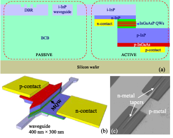
Figure 4. (a) Schematic illustration of the twin-guide active-passive integration scheme [32]. (b) 3D schematic and (c) SEM picture of the twin-guide SOA [28].
Download figure:
Standard image High-resolution imageThe active-passive integration is achieved with an adiabatic taper formed at the end of the SOA, as shown in figures 4(b) and (c). A double-taper structure is employed for high efficiency (98% according to 3D FDTD simulations) coupling in a short length (20 µm). The 300 nm thick waveguiding layer acts as the interconnection medium for all active and passive devices. The waveguide layer supports deep (300 nm complete etch) and shallow (120 nm partial etch) structures, e.g. for sharp bends and fiber grating couplers, respectively. The index contrast of such IMOS waveguides is very similar to that of SOI waveguides, therefore resulting in similar passive device dimensions and performances (see more details in section 7).
All active (such as an SOA) and passive (such as an arrayed waveguide grating (AWG)) devices, no matter their complexity or layer stack, always use the single-mode waveguide (400 nm × 300 nm) as the input/output interface. This common interface helps to transform the various active/passive devices into standardized building blocks (BBs), all of which can be interconnected by simple photonic wires (single-mode waveguides).
Based on this scheme, high-gain twin-guide SOAs with eight QWs have been experimentally demonstrated. With no heat sink present, the SOAs showed a net modal gain of up to 110 cm−1 at an injection current density of 4 kA cm−2 [28], which is comparable to those from conventional InP SOAs. Using this SOA and other passive BBs in the IMOS platform, various types of membrane lasers were successfully demonstrated at RT and CW operation, see section 4.1.
2.2.2. Ultra-compact twin-guide.
An even higher confined and more compact version of the twin-guide structure has also been investigated [33, 34]. The twin-guide scheme in figure 4 has shown that the p-cladding layer is the major limitation to the optical confinement. In order to enhance the optical confinement, the total thickness of the p-doped InP and InGaAs layers is designed to be only 400 nm, as shown in figure 5. This value is almost half of the previously discussed twin-guide scheme and 1/5 of the thickness used in the generic platforms. The resulting diode structure has an ultra-compact cross-section of 700 nm in width and in height. The small cross-section enabled ultra-short taper structures between active and passive cores. A transmission efficiency of 95% is achieved with only 8 µm taper length.

Figure 5. Cross-section of a fabricated ultra-compact twin-guide SOA [34].
Download figure:
Standard image High-resolution imageOn the other hand, such a compact diode puts more challenges on the optoelectronic performances. To achieve a top-contacted sheet-resistance-free p-contact, the p-doped layers were grown as the first layer on substrate. The p-dopant Zinc will diffuse much more into the active core and create non-radiative recombination centers, due to the reduced p-InP cladding thickness and much longer diffusion time in the metal-organic vapor phase epitaxy (MOVPE) reactor. A more detailed discussion can be found in section 3.2.1. Moreover the metal electrode is brought closer to the optical mode, resulting in an order of magnitude increase of the overall modal loss (50 cm−1 in this diode vs. 3 cm−1 in the larger-size twin-guide diode (section 2.2.1)). Pulsed operation of lasers built with this ultra-compact SOA has been demonstrated. Further optimization of the epitaxy and reduction of optical loss are needed to enable CW operation.
3. Membrane technologies
The InP membranes, with high similarities in index contrast and critical dimensions to silicon photonics, share some of the process challenges with the latter, for instance the need for a defect-free bonding process, wafer-scale precision patterning and etching uniformity, etc. On the other hand, in InP membranes, all photonic components are contained, allowing more complexed topologies as well as more creativities. In this section we discuss the process technologies of the InP membrane platforms. We identify the key challenges, the current status of solving them, as well as unique opportunities in the processing of InP membranes.
3.1. General process flow
In silicon photonics, the III–V materials are bonded (or epitaxially grown) and processed after the entire silicon photonic circuit process flow [11, 35–37]. The material and process chemistry of the silicon and III–V are incompatible, leading to a back-end-only process. In InP membranes, such constraints in the process flow are eliminated, since all epitaxies are for the lattice-matched III–V material system. This gives huge flexibility to the process technology development, leading to two major process strategies for the lateral and vertical diodes, respectively.
3.1.1. Top-side regrowth processing for lateral diode scheme.
As mentioned in section 2, the total thickness of the lateral diode membrane devices is only several 100 nm. In this section on the lateral diode scheme, we discuss the process flow based on a typical thickness of 270 nm.
The process flow has been summarized in figure 6. The initial wafer consists of GaInAsP/GaInAsP five QWs sandwiched by InP cap layers to supress the surface recombination. Under the bottom InP layer, p-GaInAs contact layer as well as InP and GaInAs etch stop layers are formed on InP substrate. Note that the p-GaInAs contact layer becomes the top side after bonding. A molecular beam epitaxy (MBE) system is used with Be as p-type dopant, which has less diffusion. The importance of this will be explained in section 3.2. Using the initial growth, three steps of selective regrowth by MOVPE are carried out for waveguide regrowth, n-InP side cladding regrowth, and p-InP side cladding regrowth. After the growth, wafer bonding to Si substrate is carried out. The bonding technologies will be explained in the section 3.3. After InP substrate removal by wet chemical etching, selective etching of unnecessary contact layer is carried out, followed by metal deposition. Finally, a surface grating is formed with electron beam (EB) lithography and wet chemical etching for the DR structure.

Figure 6. Fabrication process of lateral diode membrane DR lasers.
Download figure:
Standard image High-resolution image3.1.2. Double-sided processing for vertical diode scheme.
For the vertical diode scheme, the so-called double-sided processing technique [29, 38, 39], a combination of pre- and post-bonding processes and the creation of layers and structures from both sides of the membrane, has been employed. The process flow is depicted in figure 7. First the epitaxy wafer containing the twin-guide diode structure is grown by MOVPE. Deeply etched markers, half of the SOA structure and active-passive tapers are realized. Metal contacts are deposited on p- and n-contact layers, concluding the pre-bonding processes (see figure 7(a)). Next, wafer bonding is performed using the benzocyclobutene (BCB) polymer as the bonding interface. After the bonding, the InP substrate and etch stop layers are removed wet chemically, exposing the other side of the membrane (see figure 7(b)). The post-bonding processes include the second half of the SOA structure, deep and shallow passives and gratings (see figure 7(c)). Finally the metal electrodes buried in the bonding layer are opened for electrical contacting (see figure 7(d)).

Figure 7. Fabrication process of vertical diode twin-guide SOAs and passives [29].
Download figure:
Standard image High-resolution imageBCB polymer as the bonding interface. After the bonding, the InP substrate and etch stop layers are removed wet chemically, exposing the other side of the membrane (see figure 7(b)). The post-bonding processes include the second half of the SOA structure, deep and shallow passives and gratings (see figure 7(c)). Finally the metal electrodes buried in the bonding layer are opened for electrical contacting (see figure 7(d)).
This double-sided processing uniquely offers an extra degree of freedom in the design of membrane photonic devices. Structures realized on the backside of the membrane can significantly boost the optical and optoelectronic performances of the devices. One can find examples of using this technology for highly efficient surface gratings and ultrafast photodiodes in sections 7 and 5, respectively.
3.2. Epitaxy
3.2.1. Dopant control in thin membranes.
As shown in section 3.1, the epitaxy of the InP membranes uses typically MOVPE for growing the active-passive layer stacks. MOVPE is essential for the butt-joint regrowth process. In MOVPE processes, zinc diffusion in InP is a well-known phenomenon [40]. It will be more detrimental in the membranes as the distance between the heavily doped p-contacts and the active core is much less than in conventional diodes used in generic InP and hybrid III–V/Si platforms. In conventional SOAs the problem is not so obvious because of their much thicker intrinsic and lightly p-doped InP cladding layers in the order of 2 μm. In membrane SOAs, special attention must be paid to the diode design, as the high optical confinement brings not only the benefits, such as higher QW confinement and enhanced RF performance, but also the challenges to control the doping profile in layers of only a few hundreds of nanometers thick.
A detailed investigation on the zinc diffusion was carried out on the MOVPE grown layer stack of the ultra-compact twin-guide SOA (section 2.2.2). In this layer stack the heavily doped p-contacts are only about 400 nm from the non-intentionally doped (n.i.d.) active core. Figure 8 shows the secondary-ion mass spectroscopy (SIMS) result on the layers of interest, including the n.i.d. InP waveguide layer (a), n-contact layers (b), n.i.d. active core (c), p-doped InP cladding (d) and heavily doped p-contact layers (e). It can be seen that in the layers (c and g) adjacent to the p-doped layers (d, e and f), there is significant zinc diffusion. The zinc concentrations in iii and vii layers are around 6 × 10¹⁶–1 × 1017 cm−3 after the diffusion, which is 1–2 orders of magnitude higher than the non-intentional background doping of the reactor (<1016 cm−3). The diffused dopants are interstitial therefore forming non-radiative recombination centers [41]. The induced absorption loss can be as high as 10 dB cm−1 at 1550 nm wavelength, according to [42].

Figure 8. SIMS results on a compact membrane SOA layer stack, comparing between layers grown with zinc (MOVPE) and Beryllium (MBE). The layers shown are (a) InP waveguide layer, (b) n-doped InP and Q1.25 layers, (c) Q1.58 active layer, (d) p-doped InP layer, (e) p-doped InGaAs contact layer, (f) InP sacrificial layer, (g) InGaAs sacrificial layer. Note that for very thin layers (e.g. e and f) the true peak concentration may be underestimated due to profile broadening by SIMS.
Download figure:
Standard image High-resolution imageVarious solutions have been proposed to suppress the zinc diffusion, including using Al-containing compounds instead of InP to suppress zinc diffusion [43] as well as zinc kick-out by group III interstitials [44], use of other less diffusive p-dopants (such as carbon and beryllium) [45–47] and adding diffusion spacer layers [48]. Some of the methods can be highly tool dependent. The beryllium doping in MBE appears to be a promising alternative to the zinc. The measured BE concentration in an MBE-grown twin-guide SOA layer stack is also shown in figure 8. It is clear that the Beryllium dopants have negligible diffusion even across interfaces with very high doping step changes. This also potentially enables the p-side first growths, making double-sided membrane integration (different active functionalities, such as SOA and uni-travelling carrier (UTC) photodiode, integrated at either side of the membrane and without the need of regrowth, as envisaged in [34, 39]) possible. However MBE is regarded as less attractive to the industry as compared to MOVPE, due to the throughput bottleneck. A practical solution can be a hybrid growth, i.e. growing only the most critical layers in MBE and the rest in batches in MOVPE. This approach has been applied to the process flow of the lateral diodes (see section 3.1.1).
3.2.2. Regrowth and butt-joint integration.
For the membrane structure, especially for the lateral junction scheme, the BH structure and waveguides are formed by MOVPE regrowth technology. Two regrowth strategies have been investigated by Tokyo Institute of Technology (Tokyo Tech) and by Nippon Telegraph and Telephone, respectively. The former approach implies regrowth on an InP substrate and transfer of the membrane to silicon carrier with a bonding [49]. The latter approach first bonds a single-epi InP wafer to silicon and performs a regrowth process on the InP/Si hybrid wafer [50]. Both approaches regrow similar materials with similar dimensions.
The regrowth processes are not so different compared with the conventional regrowth for generic InP platforms. But there are a few special considerations when performing regrowth for membrane structures. The first consideration is the relatively small thickness which need to be regrown. In this case any thickness variation induced by the regrowth (for instance due to the growth enhancement effect [51]) will be significant to the optical performance of the membrane waveguides. Thus the etching process, which removes the original epi materials for regrowth, is of critical importance. This etching process must create an undercut as a reservoir for the excess atoms at the mask edges. Both the depth and the angle of the undercut are crucial. Optimization performed at Tokyo Tech has revealed that, when using a chemical solution of H2SO4:H2O2:H2O = 1:1:40 for 11 min for the etching, an undercut with a depth of 165 nm and mesa angle of 50° is achieved [52]. This condition results in a smooth regrown surface, as shown in figure 9.
Figure 9. SEM images of cross section of butt-joint regrowth [52].
Download figure:
Standard image High-resolution imageAnother consideration is the regrowth interface. This is especially critical for the lateral diodes, since the regrowth interface, such as the interface between side cladding layers and active layers, experiences current flow. Thus any non-radiative recombination layers created during etching and exposing the interface needs to be removed. Especially, this is critical in the case of AlGaInAs active layers, which can be easily oxidized. To overcome this, reducing the product of surface recombination velocity and carrier lifetime (S×τ) is important [53]. This S×τ product can be estimated by plotting the slope efficiency of spontaneous emission below threshold current. The values can be varied through different surface cleaning conditions (wet cleaning as well as in-situ chamber annealing). For example, in the Tokyo Tech's MOVPE chamber, the value of S×τ could be as low as 15 nm for in-situ chamber annealing under PH3, 650 °C for 45 min, although the value is about 1000 nm for in-situ chamber annealing under AsH3, 650 °C for 45 min [54].
3.3. Bonding
All types of InP membranes need to be bonded to a carrier wafer (typically silicon) with an optically transparent buffer layer in between. Two major bonding techniques have been used for the InP membrane, namely the BCB adhesive bonding [55, 56] and direct bonding [50, 57–59]. The exact process details of the used bonding process highly depend on the InP membrane structure, the possible need of interconnection to the silicon carrier and optical electrical thermal co-design. In the table 1 we aim to summarize the advantages and disadvantages of the two bonding techniques, which will help make the right choice for developing a specific platform.
Table 1. Comparison of adhesive bonding and direct bonding for InP membrane.
| Adhesive bonding | Direct bonding |
|---|---|
| ✓Full wafer scale | ✓Full wafer scale |
| ✓High topology tolerance (success up to 6 μm topology on each side [60]) | ✓Better heat sinking |
| ✓Accept wide range of material systems | ✓Better reliability of the bonding interface |
| ×Deformation due to thermal expansion mismatch and processing histories [61] | ×Surface flatness of 1 nm, otherwise chemical mechanical polishing process is needed |
| ×Relatively poor thermal conductivity of the BCB | ×Annealing process required |
| ×Thermal budget limited by BCB glass transition | ×Management of voids at interface [62] |
Thanks to research efforts, some disadvantages can now be solved. For example, recently, the authors at Tokyo Tech succeeded to realize room temperature direct bonding for membrane structure by Si-nano film assisted surface activated bonding [63]. Very thin (few nm) Si film deposited by spattering in the same chamber as where the bonding takes place enables surface activation to achieve room temperature direct bonding. Also, the authors at TU/e have developed a BCB bonding process to bond InP membrane wafers on CMOS electronics wafers ([64], see section 8). The process has been optimized such that all the high-temperature processes fall within the thermal budget of the CMOS electronic devices and the thermal expansion mismatch of the two wafers is compensated, resulting in a very accurate alignment (<4 µm) between the photonic and electronic devices.
3.4. Lithography
3.4.1. Enhanced EB lithography.
EB lithography is a major method for fabricating photonic nanostructures. For membrane photonic devices which have large index difference between core and cladding layers, high quality lithography is more important than that for conventional photonic devices. To realize this high quality lithography, thinner photoresist thickness is preferable to reduce line edge roughness of photoresist patterns, which gives smaller side-wall roughness of waveguides. However, we need enough thickness to act as a mask during the etching of waveguides under consideration of etching selectivity between photoresist and semiconductor. To reduce resist thickness and increase etching selectivity, simultaneously, introduction of C60 to resist is effective [65, 66]. Figure 10 shows SEM images of waveguides etched with ZEP-520 A photoresist as a mask. The image shown in figure 10(a) is the result with the resist contained C60. Compared with the etching result without C60, better etching verticality was achieved. The etching selectivity is as twice high as that for conventional photoresist.
Figure 10. SEM images of waveguides after dry etching with two different photoresists: (a) 0.1%wt-C60 in ZEP-520 A and (b) pure ZEP-520 A [66].
Download figure:
Standard image High-resolution imageImproved waveguide propagation loss in the membrane waveguides has been demonstrated by several groups using the enhanced C60/ZEP resist. Researchers at Tokyo Tech and TU/e have reported reduced losses in C60/ZEP resist patterned silicon nanowires [65], InGaAsP membrane [56] and InP membrane [67], with a record of 2.5 dB cm−1 in the electron-beam lithography (EBL) patterned InP membrane [68].
Moreover, the C60/ZEP resist also helps in maintaining the shape of the nanostructures. As observed in [67], the C60/ZEP resist has an improved thermal stability during the baking process, which helps to maintain the sub-100 nm critical dimensions of the gap in the micro-rings and the gratings in the distributed Bragg reflectors (DBRs).
3.4.2. Deep UV scanner lithography.
InP membrane photonics allows for devices with nano-scale features due to the tight optical confinement in the membrane. A PhC waveguide reflector with holes down to 110 nm radius, and DBRs with 120 nm linewidth are examples of such nano-scale devices. Currently EBL is used to pattern these small features [67]. However this process suffers from accuracy drift due to long exposure times and it is challenging to optimize very high-density circuits due to secondary electron scattering exposing resist up to 30 μm away from the exposed feature.
SOI has similarly tight optical confinement. One can therefore expect similar passive optical devices in SOI and InP membranes with comparable dimensions and performance. Nano-scale features in SOI also used to be made using EBL. Optical loss was significantly reduced by moving to 193 nm immersion lithography [69] and now benefit from the advanced lithographic capabilities of modern silicon foundries. Similar performance enhancement can be expected in InP photonics as the optical lithography processes for InP have moved from contact lithography and 245 nm lithography to a 193 nm scanner process. Recently the performance of AWGs in the generic InP platform was much improved by making use of an ASML 193 nm scanner lithography tool, which demonstrated patterning of lines down to 90 nm on an InP substrate [70].
Recently the 193 nm scanner process has been adapted for the IMOS platform. The process can efficiently print nanostructures at a full wafer scale. A picture of a 3 inch IMOS wafer, patterned with the scanner and being probed with two vertically placed optical fibers, is shown in figure 11. DBRs with dimensions down to 120 nm and PhC waveguide reflectors with holes down to 110 nm have been successfully patterned [71]. Record low-loss waveguides [71] and significant improvements on AWG key parameters [72] have been reported (see sections 7.1 and 7.2).
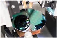
Figure 11. Picture of a 3 inch IMOS wafer patterned by the 193 nm DUV scanner [29].
Download figure:
Standard image High-resolution imageFurther improvement to the pattern profiles with the 193 nm scanner tool was demonstrated by reflowing the photoresist [71], a technique originally proposed by Kobayashi, et al [73]. After hard baking, the photoresist is exposed to an organic solvent atmosphere that softens the edge of the photoresist. When the photoresist is removed from the solvent atmosphere, the surface tension smoothens the photoresist pattern. Using this technique, the line edge roughness of typical IMOS features was reduced, especially for narrow gratings. This may lead to even lower propagation losses in the future.
3.5. Metallization
The enhanced optical confinement in the membrane-allowed for smaller diodes, which however makes the distance between the metal electrodes to the optical mode a very critical parameter. A typical example is the UTC-PD on IMOS (see section 5.2), where the position of the n-electrodes is a trade-off between optical loss and electrical bandwidth. Researchers at TU/e has developed a novel Ge/Ag ohmic contact for n-type electrodes with reduced optical loss [74, 75]. Compared to conventional Ni/Ge/Au based n-type electrodes, the Ge/Ag electrode showed an order of magnitude lower optical absorption loss at 1550 nm wavelength, while still maintain excellent contact resistance (10−7–10−8 Ωcm2) to InP and InGaAs(P) materials.
Metal stacks may spike deep into the semiconductor materials and form metallic alloys which are even closer to the optical mode. It is discovered also in [74] that the Ge/Ag metal stack shows much less spiking into the semiconductors during annealing, as compared to the Ni/Ge/Au stack. After an annealing at 400 °C for 15 s, the depths of spikes into the InP membrane are 25 nm and 300 nm for Ge/Ag and Ni/Ge/Au stacks, respectively. The much-reduced spiking depth in Ge/Ag offers a promising electrode solution with minimized influence on the optical mode.
An alternative technique to suppress the metal spiking is to precisely control the alloy formation. This can be achieved by using an ultra-thin (e.g. 20 nm of Ni) alloy formation layer on top of the semiconductor membrane during annealing [76]. A uniform alloy is formed, which can support further deposition of the full metal stack. The advantage of this technique is the uniform and controlled metal-semiconductor interface, which can prevent optical scattering at random spikes formed by an uncontrolled alloying process.
3.6. Nano opto-mechanics
When using the correct acids, there is an excellent etch selectivity between InP and its ternary and quaternary compounds. Therefore, it is possible to utilize (part of) the existing heterostructure layer stack in active devices and create wet-etched cantilever structures. Besides, doping III–V materials for the purpose of electrostatic actuation is easier than that in silicon devices. These factors create a unique opportunity for realizing nano-opto-electro-mechanical systems (NOEMS) integrated into the InP PICs.
Recently a novel NOEMS scheme has been demonstrated on the IMOS platform at TU/e. The compact SOA diode and the high optical confinement have enabled a vertically coupled waveguide system [77], as shown in figure 12. Based on this technology, highly efficient phase modulators and ultrawideband displacement sensors have been developed, see section 6.2 and 9.3, respectively.

Figure 12. (a) Schematic illustration of the vertically coupled waveguide NOEMS on IMOS. (b) Picture of a fabricated device [77].
Download figure:
Standard image High-resolution image4. InP membrane light sources
4.1. Lasers constructed with an independent SOA building block
The twin-guide SOA on IMOS offers seamless integration with submicron passive waveguides (see section 2.2). This allows the SOAs to be connected to a large variety of unique passive components such as micro-ring filters, PhC mirrors, ultra-sharp bends, etc, many of which are not available in conventional InP platforms due to the weak optical confinement of the latter. Using the single-mode membrane waveguide as the connecting interface, the SOAs and the passive components can be optimized individually and assembled to construct various types of laser cavities, as illustrated in figure 13. This shares the same philosophy with the generic InP photonic integration [4], and so far several lasers have been demonstrated on the IMOS platform. A summary of the performance details of the demonstrated lasers on IMOS can be found in [29].
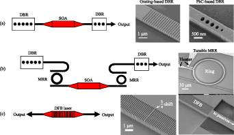
Figure 13. (a) Schematic illustration of the membrane DBR laser, with SEM pictures showing the grating-based and PhC-based DBR mirrors. (b) Schematic illustration of the membrane tunable laser, with SEM picture showing the thermally tunable micro-ring resonators. (c) Schematic illustration of the membrane DFB laser, with SEM pictures showing the quarter-wavelength shifted DFB grating and the active-passive interface.
Download figure:
Standard image High-resolution imageOne of the most straightforward laser design realized is the DBR laser [78]. The cavity is formed with two PhC-based DBR reflectors [79] in the passive areas of the circuit (see section 7.2). An alternative realization of the DBR is based on conventional gratings [80]. By simply adjusting the number of periods, the reflectivity can be flexibly tuned. For instance, on the front side these reflectors can have five periods which gives 60% reflectivity. On the back side the PhCs have eight periods which gives 99% reflectivity [79]. Such high reflectivity and the tuneability are not offered in the conventional InP platforms. The fabricated conventional DBR and PhC reflectors are shown in figure 13(a). Knowing the achievable optical gain from the amplifier and the reflectivity from the DBRs, the length of the laser can be determined to meet the desired laser specifications [81]. The realized PhC DBR laser device showed 20 mA threshold current (2 kA cm−2 threshold current density) with 1 mW power in the waveguide [82]. This basic DBR laser configuration can be used for designing more complex devices, such as mode-locked lasers with centimetre long cavity length, leveraging the ultra-sharp bends offered in the InP membrane platform.
As an extension to the simple DBR lasers, we demonstrated a Vernier tunable laser based on the PhC DBR cavity. The tunability is realized by two thermo-optically tunable micro-ring resonators with slightly different FSRs, acting as wavelength selective elements in the cavity, as shown in figure 13(b). The 3 dB bandwidth of the optical gain from the amplifier is over 50 nm [28], which is sufficient for tunable lasers. All the elements except the SOA are fabricated in a single passive etching step. Tunable lasers in the IMOS platform show tuning of the lasing wavelength up to 25 nm when exploiting the Vernier effect [83]. The tuning coefficient is 2.5 nm mW−1 and can be further improved by optimizing the design of the thermo-optic heaters. Furthermore, the SMSR of the device ranges from 31 dB to 44 dB within the tuning range, which makes the devices suitable for WDM systems. Measured lasing spectra of the tunable laser are depicted in figure 14(a) with a wavelength tuning interval of 5 nm.
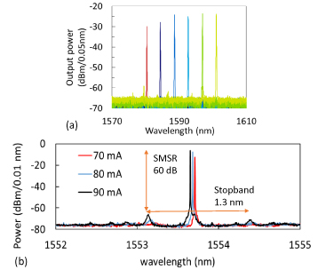
Figure 14. Lasing spectra of (a) the Vernier tunable laser and (b) DFB laser on IMOS [32].
Download figure:
Standard image High-resolution imageFurthermore, a membrane quarter-wavelength shifted DFB laser has been demonstrated with more than 60 dB SMSR [84]. The lasing spectra are plotted in figure 14(b) for three different pump currents. The DFB grating is defined on top of an SOA area using the same etch depth and processes as for the DBR reflectors, as shown in figure 13(c). Unlike the SOI platform where gratings are etched in silicon and have a bonding interface from the III–V gain structure, the grating etch in IMOS is performed above the SOA structure. Thus, the coupling strength is insensitive to the bonding process and can be controlled more precisely. The DFB laser showed 2.5 kA cm−2 threshold current density and 20 mW total output power in the waveguides [29]. The high SMSR values of 60 dB in the demonstrated laser is a good indicator of the low noise operation.
With the continuous expansion of the passive component portfolio in the IMOS platform, more types of lasers can be designed using the generic integration concept. The wafer-scale technology can enable future membrane-based multi-project wafer (MPW) runs [85] acting as a vehicle for application-oriented laser circuit designers.
4.2. DR lasers for low threshold, high efficiency and high speed
Whereas the IMOS platform aims at high flexibility in building a laser cavity, the DR lasers presented in this section have a focus on extreme speed and energy performance for the interconnect applications using a fixed laser cavity concept. The most important design considerations are discussed below.
For the purpose of on-chip optical interconnections, the energy cost (which is the energy to send 1 bit) of a light source should be less than 100 fJ bit−1 [86], which corresponds to an operation current of 1 mA, considering a voltage of 1 V and a speed of 10 Gbps. Also, for detection by PIN photodiodes, more than −13 dBm of received power is desired to achieve a low bit error rate [87]. Considering a 5 dB loss budget in the circuits, the output power of the lasers should be more than −8 dBm (0.16 mW). Therefore, an output power of 0.16 mW at the operating current of 1 mA, as well as >7.7 GHz bandwidth (for 10 Gbps), are needed. These are quite challenging values for conventional lasers.
To reduce the threshold current of lasers, of course, introduction of higher reflectivity (lower mirror loss) is effective. On the other hand, too high reflectivity makes the output efficiency too low. In case of DFB or DR lasers, the effective reflectivity depends on their cavity length. Figure 15(a) shows the DFB section length dependence of the threshold current and the external differential quantum efficiency of a membrane DR laser. The stripe width and the core thickness are 1 µm and 250 nm, respectively. The grating depth is 50 nm, which corresponds to a coupling coefficient κ of 1800 cm−1. The internal quantum efficiency and the waveguide loss are assumed to be 75% and 42 cm−1, respectively. The minimum threshold current reaches to 155 µA at a cavity length of 22 µm. Although the external differential quantum efficiency increases with shorter cavity lengths, the threshold current drastically increases as well. Actually, the value of the threshold current is not important for applications, but the operating current is. Figure 15(b) shows the DFB section length dependence of the required bias current to obtain an output power of 0.16 mW. Note that the coupling coefficient κ at each section length is adjusted to achieve minimum values at each length. We can see that the optimum section length in terms of operating current becomes much shorter than that in terms of minimum threshold current as shown in figure 15(a). We also need to consider the modulation bandwidth. In figure 15(b), the current for the output power of 0.16 mW cannot achieve enough bandwidth for DFB section length of >40 µm. Figure 15(c) shows the DFB section length dependence of the required bias current to obtain a modulation bandwidth of 7.7 GHz for 10 Gbps operation. The required bias current for the bandwidth of 7.7 GHz cannot produce at the same time enough output power for DFB section lengths of <50 µm.

Figure 15. DFB section length dependence of (a) the threshold current and the external differential quantum efficiency of a membrane DR laser with a core layer thickness of 250 nm; (b) the required bias current for a light output power of 0.16 mW; (c) the required bias current for a modulation speed of 10 Gb s−1; (d) total power consumption for the required light output power and that for 10 Gb s−1 operation [87].
Download figure:
Standard image High-resolution imageIn the above discussion, we do not consider power consumption, which is also important for real applications. To consider power consumption, we have to take into account the operating voltage, which is determined by electrical resistance. A very short section length gives a higher electrical resistance. Therefore, the electrical resistance is another trade-off factor. Figure 15(d) shows the total power consumption as a function of the DFB section length, in terms of output power and modulation speed. As we can see, the output power limits the power consumption for lengths <50 µm and the modulation speed limits it for longer sections. The power consumption reaches a minimum at the section length of 19 µm. At this length, 63% of the total power consumption is due to Joule heating. To reduce the total electrical resistance, reducing the electrical resistance of the p-type side cladding is a key. Mainly, we have two points to be optimized. One is the doping level. This has a trade-off with the waveguide loss. The other one is the distance between the edges of the electrodes and the active region. This has a trade-off with the waveguide loss, too, since a too small distance results in an optical field overlap with the electrode metals. By optimization of these points, the energy cost can be reduced to 63 fJ bit−1. In addition to this, if we can reduce the system loss budget to 1 dB, and increase the modulation speed to 20 Gbps, an energy cost of 21 fJ bit−1 can be achieved in theory.
The characteristics of a recently fabricated DR laser [25] are shown in figure 16. Figure 16(a) shows a SEM cross-sectional view of the fabricated DR laser. The threshold current and external differential quantum efficiency are 0.21 mA and 32%, respectively, under room temperature CW condition, as shown in figure 16(b). The stripe width, DFB section length and backside DBR section length are 0.8 µm, 32 µm, and 50 µm, respectively. Figure 16(c) shows the small signal modulation characteristics. At a bias current of 0.77 mA, the bandwidth f3dB reached 11.2 GHz, which is sufficient for 10 Gbps operation. From this small-signal modulation response, the relaxation oscillation frequency fr and the 3 dB bandwidth f3dB as a function of the square root of the bias current can be obtained. The slopes of fr (modulation current efficiency factor: MCEF) and f3dB were 12 GHz mA−1/2 and 15 GHz mA−1/2, respectively. These values are quite high compared to conventional DFB and DR lasers. With this device, eye opening at a bit rate of 20 Gbps could be observed with a bias current of 1.06 mA. Bit error rates as low as 6.4 × 10⁻¹⁰ are obtained and the energy cost of this condition reaches 93 fJ bit−1.
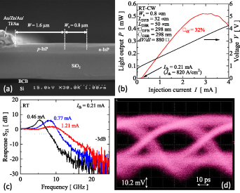
Figure 16. (a) SEM sectional view of the fabricated DR membrane laser. (b) The current-light and current–voltage characteristics. (c) Small signal modulation characteristics and (d) 20 Gbps Eye diagram at the bias current of 1.06 mA [25].
Download figure:
Standard image High-resolution image4.3. Nanopillar-cavity light sources
Nanoscale light sources with metal cavities have been investigated intensively for slightly more than one decade. In these devices, the metal cladding is employed to achieve a strong spatial confinement, while preserving a sufficiently high quality factor to achieve lasing. Furthermore, the metal cladding can efficiently remove the heat generated by the diode electrical resistance. Early work on metal cladding cavities exploited two configurations: nanopillars and metal–insulator-semiconductor-insulator-metal waveguides. Both configurations achieved sub-wavelength confinement in at least one dimension and allowed electrical injection which is fundamental for most of the practical applications [88, 89]. Later, some of these structures demonstrated CW operation at room temperature [90].
More recently, significant progress has been made in the field of metal cladding nanopillars in InP membrane platforms, which allowed the outcoupling of optical power into a single-mode InP waveguide channel [91, 92]. Such a waveguide integration is a significant advancement in this field, since the nanopillar light sources can be connected directly to the wide portfolio of active and passive BBs offered in the same InP membrane platform. This ranges from higher-power amplifiers and high-speed detectors to filters and switches. Highly integrated, fully functional nanophotonic circuitry then becomes feasible.
In [91], light coupling from the nanopillar to the low-loss waveguide was achieved through the evanescent field. An SEM picture of the fabricated nanopillar, integrated on top of an InP membrane waveguide and before being encapsulated by the metal cladding, is depicted in figure 17. The devices are characterized through grating couplers, which are standard BBs of the InP membrane platform. While these waveguide-coupled nanocavities have not reached lasing due to a detrimental combination of high non-radiative recombination and a dedicated waveguide (cavity loss channel), the devices operated as nanoLEDs with record on-chip external quantum efficiency [91] (10−4 and 10−2 for room-temperature and 9.5 K, respectively) and tens of nW optical power, far exceeding the previous nanoscale LEDs. Contrary to cavity-less nanoLEDs which could support a high number of confined and radiating modes, metal-cavity nanoLEDs support very few optical modes, therefore the radiation efficiency into the mode of interest can be drastically improved.
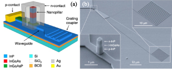
Figure 17. SEM picture of a fabricated nanopillar on InP membrane waveguide [91].
Download figure:
Standard image High-resolution imageCapsule-shaped nanopillar cavity with curved metallic facets has been first proposed in [93]. The enhanced confinement of the cavity modes can lead to an improved quality factor and a reduced threshold. This idea has been further elaborated in [92] with a similar evanescent-field based waveguide output. Preliminary results have shown spontaneous emission successfully generated under electrical pumping and coupled and collected from the InP waveguide [92].
Further technological improvements in order to achieve lasing in these devices include novel metal claddings and contacts (e.g. silver-based contacts which are able to provide low electrical and optical loss at the same time) [74]. Better passivation techniques can also result in much improved cavity performance in such nanopillars, which have exceptionally high surface-to-volume ratios. For example, colleagues at TU/e have demonstrated a surface recombination velocity as low as 260 cm s−1 in InGaAs, through a combined passivation process of ammonium sulphide and SiO2 sealing [94]. Finally, the atomic layer deposition technology can be used to significantly improve the optical quality and uniformity of the deposited metals [95, 96] as well as to reduce the interface damage and break the feature size bottleneck in conventional lift-off processes [97, 98].
5. Photodiodes
5.1. Photodiodes based on membrane laser stacks
Photodiodes are another important device in PICs. Structures similar to the membrane laser can be used. Figure 18(a) shows a microscope image of a fabricated membrane photodiode with a lateral diode scheme [99, 100]. The structure is basically as same as that of the DR membrane lasers, except for the introduction of a GaInAs bulk absorber instead of the QWs. The responsivity of 0.95 A W−1 was achieved with a stripe width of 0.7 µm and a device length of 30 µm. Using this device, a bit error rate measurement has been performed, as shown in figure 18(b). Clear open eye diagrams and error free operation are achieved up to 20 Gbps. For membrane photodiodes, the detection speed is limited by the carrier transition time, especially for holes, due to their low mobility, and by the capacitance. These parameters are determined by stripe width and device length. The carrier transition time and capacitance have trade-off relations in terms of the stripe width. At narrow stripe widths, the capacitance is the dominant factor. At wide stripe width, the carrier transition time is the dominant factor. A shorter device length is better in terms of capacitance. However, a shorter length gives a lower responsivity. To maintain enough responsivity, even with short device length, introductions of DBR and PhC structures were proposed and demonstrated [100, 101]. With these structure, fF-level capacitance can be realized. Such small capacitances may enable the realization of trans impedance amplifier-less operation for low power consumption detection.

Figure 18. (a) A microscope image of a fabricated membrane photodiode. (b) Bit error rate and eye diagrams of the device [99, 100].
Download figure:
Standard image High-resolution imageWith combinations of lasers, photodiodes and waveguides, a first fully integrated on-chip interconnect PIC has been demonstrated [102] as shown in figure 19. A DFB laser and a PIN-photodiode are connected by a 500 µm long GaInAsP membrane waveguide. A bit error rate of 6 × 10⁻⁷ was achieved with a bias current of 2.5 mA for the laser and a bias voltage of −3 V for the detector. At the moment the performance of each component in this PIC is not as high as that of discrete devices. Electrical isolation may be an important factor to improve the overall performance.

Figure 19. First on-chip interconnect PIC with membrane components [102].
Download figure:
Standard image High-resolution image5.2. Ultrafast UTC photodiodes
In PIN photodiodes, the photogenerated holes with their slow transit velocity will limit the highest achievable electrical bandwidth. UTC photodiodes were proposed to overcome this bottleneck [103]. Realizing UTC photodiodes on photonic membranes brings additional advantages regarding the optimization of efficiency and speed.
A substrate-free UTC photodiode on the IMOS platform has been developed [104]. The device uses the IMOS waveguide layer as the intrinsic layer, which is sandwiched between a p-doped InGaAs absorption layer and an n-doped InP collector layer. P- and n-metal electrodes are designed at opposite sides of the membrane, respectively, using the double-sided design and processing technique. The cross-section schematic is depicted in figure 20(a). The tight optical confinement in the InP membrane has led to a high responsivity (0.8 A W−1) due to strong overlap with the absorption layer, low RC contacts (junction capacitance < 10 fF) and taper-free butt-joint integration with nanophotonic waveguides. The double-sided metal electrodes significantly reduce the sheet resistance from the p-doped absorption layer. An electrical 3 dB bandwidth of beyond 67 GHz (instrument limit) for a 3 × 10 μm2 device has been measured (see figure 20(b)), with an extrapolated bandwidth reaching 100 GHz.
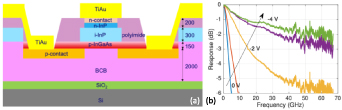
Figure 20. (a) Schematic of the membrane-based UTC photodiode and (b) measured electrical bandwidth [104].
Download figure:
Standard image High-resolution imageSuch UTC photodiodes, featuring high speed and integration with waveguides and gratings, are of high potential in optical communication (see section 9.2) and microwave to terahertz photonics applications [105].
6. Modulators
6.1. Electro-optic (EO) phase modulators
Phase control and modulation are essential in any photonic circuits. In this section we review EO phase modulators on InP membranes based on several different mechanisms. The carrier-induced effects are dominant in conventional InP/InGaAsP based phase modulators [4]. Their operation is based on a p-i-n diode structure without the active gain medium. This requires additional regrowth steps.
A promising alternative takes advantage of the high optical confinement in such membranes by creating slot waveguides filled in with EO polymers. The refractive index of the EO polymer will change under an electric field, resulting in a phase shift. Studies have been conducted intensively on silicon-based slot waveguides, leading to the so-called silicon organic hybrid (SOH) modulators [106]. The r33 coefficients in EO polymers that are used typically range from tens to several hundreds of pm V−1 [107], enabling record performances such as VπL values down to a fraction of one V mm [108], 100 Gbit s−1 data rates [106] and power consumption below 1 fJ bit−1 [109].
InP in comparison to Si features higher carrier mobility and lower optical loss at the same doping level. Therefore, InP based slot devices are capable to achieve lower optical loss with lower doping levels, while still maintaining high electrical conductivity and electrical bandwidth. Theoretical investigations on an InP membrane organic hybrid modulator has been reported in [110]. The study shows that, to achieve the same 100 GHz bandwidth, the InP membrane-based device only requires a 1/10 of the doping level that is used in SOH devices. This lowered doping level leads to a 30 times reduction in optical loss induced by free-carrier absorption (FCA).
Preliminary experiments have been carried out on a fabricated device, designed and realized on the IMOS platform [111]. The schematic cross section of the InP membrane slot modulator is shown in figure 21(a). The 300 nm thick InP membrane contains a 270 nm intrinsic waveguide core and a 30 nm n-doped (2 × 1018 cm−3) conductive layer for electrode contacting. The free carrier induced optical loss is calculated to be below 0.02 dB cm−1. The 200 nm slot width gives an optical confinement factor of 17% in the slot. After the fabrication of the slot waveguide, commercially available EO polymer with a moderate r33 value of 63 pm V−1 is applied on the device and poled. A cross-sectional picture of a fabricated device is shown in figure 21(b). A VπL value of 3 V mm has been obtained, which can be further improved by using EO polymers with higher r33.

Figure 21. (a) Schematic illustration of the slot waveguide hybrid modulator on InP membrane. (b) The SEM picture of the slot waveguide cross section, with the slot filled with EO polymer.
Download figure:
Standard image High-resolution imageAnother type of phase modulator on InP membranes is a carrier-injection phase modulators. There are also advantages of using InP-based materials for carrier injection modulators as compared with silicon. The carrier induced refractive index change in Q1.25/InP waveguides is about four times higher than that in silicon at a carrier concentration of 1017 cm−3 [112]. Therefore a much-reduced driving current for a carrier-injection phase modulator can be expected by using InGaAsP/InP membranes.
Ikku et al have proposed a lateral diode structure on a 350 nm thick Q1.25 InGaAsP membrane layer for the carrier injection modulator [112]. The p and n doping are realized by ion implantation, similar to that used in silicon devices. The first demonstration has shown good loss management (4 dB cm−1) even with dopants close to the optical waveguide and a low half-wave current-length product of 0.1 mA mm. This is lower than in silicon devices reported at the time.
This lateral current-injection phase modulator has been further developed for co-integration with an InGaAs-based MOSFET (see section 8.2). A few process steps for the modulator have been changed in the co-integration process flow. For instance, the p-doping step was changed from ion implantation of Be to Zinc diffusion by spin-on glass [57]. The co-integration has been successfully demonstrated with both the modulator and driver operating as expected [57]. However the reported current-length product is about 10 times higher than in the early work of [112], probably due to the high uncertainty of the Zinc profile. The electrical bandwidth is still yet to be demonstrated with a predicted value of over 10 Gbit s−1.
6.2. NOEMS phase modulator
Besides the conventional phase modulators which use the field and carrier effects within the semiconductor, another type of efficient phase modulator is based on a vertically coupled double waveguide system fabricated using the NOEMS technology on membrane (see section 3.6). The mechanically induced change of the coupled waveguide geometry will result in a great change of the effective refractive index.
An IMOS-based NOEMS phase modulator has been recently demonstrated [77]. The phase modulator is based on a compact twin-guide layer structure very similar to the one described in section 2.2.2. By selectively removing the active core layer, the p-doped layers form a top waveguide which evanescently couples with a bottom waveguide which is formed by the n-doped layers. A picture of the fabricated device is shown in figure 12(b). By applying a reverse bias, the electrostatic force created from the accumulated charges in the coupled waveguide system will result in a significant change of the effective index. A maximum of 4.8π phase shift has been recorded under a bias voltage of 6.5 V for a 140 µm long device [113]. An ultra-low VπL value of 0.056 Vmm can be obtained by pushing the device operation (with a 5.1 V pre-bias) close to the mechanical instability regime [77]. The electrical bandwidth of such a device is determined by the mechanical resonance frequency of the system. The reported device shows a bandwidth at the MHz level, which makes it more suited for low-energy optical switching applications [29].
6.3. Band-filling based EAM
Recently a novel operating principle for an InP membrane modulator based on the band filling effect was presented [114]. The schematic cross-section of the device is depicted in figure 22(a). By filling the conduction band, the apparent bandgap increases which can be used to modulate the optical transparency over a wide wavelength range. This is different from the quantum confined Stark effect where the absorption is modulated by changing the overlap between quantum states in a QW with an electric field, which is inherently narrow band.

Figure 22. (a) Schematic cross-section of the band-filling EAM. (b) Calculated optical absorption of the InGaAs core for different n-doping levels [114].
Download figure:
Standard image High-resolution imageFor efficient modulation of the apparent bandgap, a material with a small conduction band density of states is desirable. InGaAs fulfills this requirement for materials lattice matched to InP. For InGaAs to become transparent at 1550 nm, the electron concentration needs to be higher than 2 × 1018 cm−3. The electron concentration is modulated in a p–n junction by changing the applied reverse voltage. A reverse voltage of 1.5 V depletes 8 nm of the material. While the depletion is shallow, comparable to the dimension of a QW, the material absorption when depleted is very high. Still tight optical confinement of the mode to this thin layer is needed for sufficient extinction ratio. InP membranes are ideally suitable for integrating such a layer due to the high optical confinement.
The band-filling effect is inherently broadband (see figure 22(b)) because it is the apparent band edge that is being modulated. It is predicted that the modulator will operate on a CMOS compatible 1.5 V voltage swing, over a wavelength range of 100 nm with modulation speeds in excess of 50 Gbit s−1 and a power consumption of 53 fJ bit−1 at a length of only 80 μm [114].
7. Passive components
7.1. III–V membrane waveguide system
The high optical confinement in InP membranes leads to waveguide dimensions and bend radii comparable to those of the SOI platforms [29]. This created new opportunities for InP integrated photonics with reduced footprint, enhanced performance, as well as new functionalities.
The single mode waveguides on InP membranes have typical dimensions of 400–600 nm in width and 150–300 nm in height, when fully etched. The waveguide widths and membrane thicknesses are chosen to maintain single-mode condition with low optical loss. The materials used for the waveguide core can be either InP [67, 115], InGaAsP [56] or InGaP [116]. Typical linear propagation losses of the waveguides range from >10 dB cm−1 to below 2 dB cm−1, depending on the material for the core and the lithography process used. It has been observed that by using improved lithography processes (for instance improved EBL resist [67, 68] or DUV lithography [71], see section 3.4 for details), the linear propagation losses can be greatly reduced due to the reduction of sidewall roughness. The record low propagation loss demonstrated so far is 1.8 dB cm−1 on the InP-based IMOS platform [71], which is comparable to the typical loss value in fully etched SOI waveguides [117]. On the route to further reduction of the propagation loss, partially etched InP membrane waveguides can be considered, inspired by the 0.7 dB cm−1 achieved in partially etched SOI waveguides [117].
The high optical confinement in the InP-based membrane waveguides leads to a much-increased photon density and therefore to a reduced threshold for nonlinear processes. This makes them attractive for all-optical and quantum applications [118, 119]. However undesired two-photon absorption (TPA) and FCA co-exist in these waveguides and can be more pronounced due to the higher photon density as well as the material direct bandgap. A brief survey of the nonlinear properties in an InP membrane (IMOS platform) and a comparison with SOI can be found in [29].
A practical approach to suppress the TPA effect at telecom wavelengths is the bandgap engineering. One can increase the bandgap such that half of the bandgap is larger than the photon energy. This can be done by tuning the composition of the III–V compound [116, 120] or by replacing a large part of the passive circuits with high-bandgap dielectrics [121].
7.2. BBs portfolio
A wide range of passive BBs have been developed in the InP/GaInAsP membranes (mainly on the IMOS platform). The similar index contrast and propagation loss as in the SOI platforms lead to a similar device portfolio with comparable footprints and performances. The following list describes a number of important devices that have been demonstrated on the InP membranes.
Waveguide bends are essential for optical signal routing and building of complex devices and circuits. Conventional arc bends down to 3–5 μm radius [122] and special corner-mirror-based bends of 1 μm effective radius [123] have been reported in InP membranes. The corner mirror offers a low loss, high optical bandwidth (>100 nm) and fabrication tolerant solution for low-footprint redirecting and decoupling of the optical signals. For instance, when used in the directional couplers, the corner-mirror bends ensured smaller footprint as well as reduced parasitic coupling as compared to arc bends [124].
On-chip parasitic back-reflections can be significant in InP membrane waveguide systems due to the tight optical confinement. Back-reflections in optical couplers can be detrimental to high-precision interferometer circuits on the chip. A novel MMI coupler layout, originally proposed for the conventional InP waveguides [125], has been adapted and optimized for the IMOS platform [126]. More than 10 dB reduction of the back-reflection, as compared with the conventional MMI design, has been predicted by simulations.
In conventional InP platforms, creating controlled and broadband on-chip mirrors rely on either end facets or MMI-based reflectors [127]. The former restricts the location of the mirrors, while the latter gives a significant optical loss. On the InP membrane, a new type of on-chip mirrors based on 1D PhC has been developed [79], showing high reflectivity (>95%), broad optical bandwidth (>100 nm) and ultracompact footprint (4 μm in length).
Interfacing the InP membrane devices and circuits with the outside world, e.g. with an optical fiber or a free-space object, is facing the problem of a large mode mismatch, similar as the SOI platforms. Therefore, surface grating couplers (SGCs) are commonly used for the coupling of the light in and out of the circuits. Grating couplers on InP membranes with simple etched pitches in the waveguide show typical coupling loss of 5.5 dB [34] (using InP as the core material) and 4.2 dB [128] (using InGaAsP as the core material) to single-mode fibers. By incorporating the double-sided design and processing technique uniquely available in the InP membrane platforms, the efficiency of the grating couplers can be significantly boosted. For instance, backside metal mirrors can be deployed to harvest the light diffracted downwards, resulting in a record-low fiber coupling loss in InP membranes of 1.2 dB [129]. The grating structures can be even realized directly in a metal layer next to the InP waveguide core, using the double-sided technique [130]. An alternative way of optical interfacing is through spot-size converters (SSCs) with edge coupling. SSCs are intrinsically wavelength independent, and therefore suited for broadband coupling. Recent results demonstrated a SiOx -based SSC on InP membrane with 2.2 dB coupling loss to a fiber [131].
Wavelength multiplexing and demultiplexing devices are essential for WDM applications. AWGs have been developed on InP membranes. Such a device is highly sensitive to fabrication-induced phase errors in the arrayed waveguides and to additional losses at waveguide interfaces. It is reported that by using a DUV scanner lithography process, both insertion loss and crosstalk of the AWGs can be greatly improved (3.7 dB and −15.3 dB, respectively) as compared to those obtained with EBL (6–10 dB and −10 dB, respectively) [72, 132]. This brings the performance of the AWGs on an InP membrane close to those reported in the SOI platforms [133].
Work has also been done to reduce the footprint of the AWGs. Reflective-type AWGs have been developed on InP membrane, showing a 35% footprint reduction with no compromise on the device crosstalk and only a slight increase in the insertion loss [134]. It is worth mentioning that this device is designed by combining a standard AWG and a PhC reflector BB, and that it is realized in an internal MPW run of the IMOS platform.
Planar concave gratings (PCGs) are promising alternatives to AWGs with reduced phase-errors and better crosstalk. PCGs on an InP membrane, with DBR structures as broadband reflectors at the diffraction grating facets, have been proposed and demonstrated [135], showing −18 dB crosstalk. With improved EBL patterning on the DBR sections, a PCG with crosstalk as low as −25 dB has been reported [136].
The crystal structures in InP and its compound materials enables a new type of triangular waveguide for fabrication-tolerant polarization manipulation devices [137]. This concept has been adapted to the InP membrane (the IMOS platform) and resulted in a polarization converter with 99% polarization conversion efficiency with an ultracompact footprint (<10 μm in length) [138]. This device is now being further optimized for active-passive integration with lasers and modulators [139]. In this way, advanced functionality, such as Stokes vector modulation, can be enabled.
Plasmonic slot waveguides have also been proposed and demonstrated on the IMOS platform [140]. The metal–insulator-metal slot waveguide structure provides stronger optical interaction with the materials in the slot and requires less length as compared to conventional slot waveguides. A propagation loss of 0.43 dB μm−1 and a waveguide-to-slot coupling loss of 4.2 dB have been demonstrated from the first attempt. This BB can be valuable for high-speed optical interconnects and plasmonic sensing applications.
8. InP membrane on electronics
The substrate-free nature and high flexibility of the InP photonic membrane make it suitable for direct integration with electronics. Two main technology approaches have been investigated: heterogeneous vertical integration using wafer bonding developed at TU/e and monolithic integration of photonics and electronics in the same membrane developed at the University of Tokyo (UTokyo). In this section, we discuss in detail the latest developments in both approaches.
8.1. Heterogeneous integration on electronics
Standard techniques to combine optical and electrical functions are wire bonding and flip-chip bonding using stud bumps. These approaches however limit the electrical bandwidth, since for high frequencies the path lengths are on the order of the wavelength of the RF-signal. Furthermore, they take up a large footprint, which is at odds with the desire to reach high density integration. Monolithic integration of photonics and electronics has been also demonstrated [57]. This will be discussed in the next subsection. In that case, a compromised performance may be implied in order to realize these different functionalities in the same material stack and processing flow. The idea described here avoids these issues; based on the InP membrane technology, creating an intimate heterogeneous integration of separately realized electronic and photonic functions can be obtained.
A major advantage of using InP membrane photonics is the possible vertical combination with microelectronics at wafer-to-wafer level. The electronic circuits (e.g. CMOS) and the InP photonic circuits can be realized independently in separate fabrication processes. Therefore these processes can be kept in their optimized and standardized conditions. The hybrid integration of the two occurs in a backend process. An artist's impression on InP membrane integrated on, and interconnected to, a CMOS electronics wafer is depicted in figure 23(a) [34].

Figure 23. (a) Artist's impression of the InP membrane photonics vertically integrated with a CMOS electronics wafer [34]. (b) Photronic wafer (BiCMOS wafer with InP membrane) with SiO2 hard mask (dark blue) for etching windows into the InP membrane.
Download figure:
Standard image High-resolution imageThe integration is done by placing a photonic membrane circuit on top of an electronic circuit, which reduces the physical distance greatly. This enables a new design dimension for the hybrid devices. Short interconnects between the two circuits are a key requirement to increase the electrical bandwidth and reduce electrical power consumption. Within the European 'WIPE' project [141] researchers at TU/e have developed such a technology by integrating photonics with electronics on a wafer level. The technology uses an adhesive wafer bonding approach based on [60]. The starting point is the two wafers from the two different domains: photonics and electronics. The photonic wafer is based on InP and has a diameter of 3 inch. The electronic wafer is fabricated in a 0.25 μm SiGe:C BiCMOS process on a 200 mm (8 inch) wafer. Both wafers are made in mature foundry processes. At the end of the process the InP membrane, containing the photonic ICs, is bonded to a BiCMOS wafer (i.e. 3 inch wafers cut out from the original 8 inch wafer for size matching), containing the electrical circuits. They are electrically connected with interconnects through the adhesive bonding layer. The designs on the photonic and electronic wafers match each other, which is obtained by co-designing the InP wafer based on the layout of the BiCMOS wafer. Care needs to be taken to correct in this design for the different thermal expansion of InP and Si, since the bonding will take place at an elevated temperature.
A back-side alignment is performed before the bonding and the substrate removal. The thickness of the BCB-layer is 24 μm in total, which is essential to accommodate the topologies on the two wafers [60]. The alignment accuracy obtained with such a thick BCB layer thickness is better than 4 µm, which is sufficient for aligning the metal electrodes of the photonic and electronic devices.
Creation of interconnects and heat sinks is done after the bonding and substrate removal. Windows are etched through the InP membrane to expose the underlying InP contact pads. In figure 23(b) the bonded wafer is shown just before etching the windows into the InP membrane (covered with SiO2 hard mask patterns). The BiCMOS contact pads are opened next by etching a sloped via through the BCB. Finally, the via interconnect, connecting InP and BiCMOS contact pads, is formed by the electro-plating [142]. Figure 24 shows a photograph of a created co-integrated wafer, presenting the etched structures used to access the photonic (gold) and the electronic (aluminium) contact pads [64].

Figure 24. Picture of the InP-based photonic membrane layer with windows to access and interconnect the photonic (gold) and the electronic contact pads (aluminium). Picture credit to F Lemaitre.
Download figure:
Standard image High-resolution imageThis vertical integration concept can be further extended to a wide range of electronics, since the entire membrane-based photonic layer is completely independent from the carrier. An interesting development is the integration of an InP photonic membrane on an organic substrate [143], developed at Tokyo Tech. The feasibility study in [143] has shown that the InP membranes can be bent to a very short radius (up to 100 μm for a 200 nm thick membranes). Such a combination can enable a complete optical sensor circuit integrated on large-area, flexible and ultralow-cost electronics printed on organic and other flexible substrates [144, 145]. Potential applications include e.g. wearable smart sensors for sport and health monitoring.
8.2. Monolithic integration of electronics
Apart for the integrated photonics, the InP material system also excels at high-power and high-frequency electronics [146, 147]. Integrating InP photonics and electronics on the same InP substrate is challenging, because the large difference in dimensions and layer stacks. The InP membrane allows for more freedoms in diode structure design, which opens up a unique opportunity for a monolithic integration with electronics.
Takenaka et al from UTokyo has proposed a membrane-based monolithic integration scheme, named 'III–V CMOS platform' [57, 148, 149]. The key demonstration on this platform so far is the monolithic integration of a lateral PIN InGaAsP MZI optical switch (see section 6.1) with an InGaAs driver MOSFET in the same membrane [57, 149]. The InGaAsP membrane waveguide layer is reused as part of the MOSFET layer stack. The integration scheme has also been designed such that a significant part of the process steps is shared between the realizations of the PIN and MOSFET structures, including the dry etching, n-doping, metallization and passivation [57]. This can greatly reduce the complexity of the monolithic integration technology of completely different structures. The schematic illustration of the monolithic integration and a picture of a fabricated MZI with integrated MOSFET driver are shown in figure 25. Preliminary experiments on the monolithic MZI-driver circuit showed encouraging results, with a π phase shift under a gate voltage of 1 V [57].

Figure 25. (a) Schematic illustration of the monolithic integration platform. (b) Picture of a fabricated MZI optical switch with integrated MOSFET driver [149].
Download figure:
Standard image High-resolution imageThe single process flow on the other hand implies a compromise between photonics and electronics device performances. Relatively high optical losses in the MZI and low effective mobility in the MOSFET are observed, which suggests that further process optimization is necessary [57].
Other photonic functionalities have been demonstrated as well in this III–V CMOS platform, including waveguides and bends [122], grating couplers [128], AWGs [132] and photodetectors [150]. However, they have been fabricated so far with a photonics-only process flow. Realization using the full MOSFET process flow has not yet been shown, except for the MZI optical switch device mentioned above. Although a laser/amplifier function has not been demonstrated yet on this platform, it is suggested that the lateral laser diodes can be a feasible approach to create a complete platform [148].
9. Applications for InP photonic membranes
In this section we present several application domains in which the InP photonic membranes have a high potential.
9.1. Optical interconnects
Optical inteconnection is one of the promising applications for membrane PICs, to overcome the speed-energy bottleneck in current electrical wire connections in the electronic chips [86], which is the reason why the clock speed of commercial processors is limited to around 3–4 GHz. By replacing these electrical global wire layers with optical interconnections, such as the recent demonstration shown in figure 19, the performance of electronics improves in terms of clock speed. To realize this, ultra-low energy cost and ultra-small photonic devices are needed. Membrane PICs can be promising candidates for this, since they can achieve ultra-low energy cost, ultra-small device size and complete active-passive integration.
Extensive studies on the energy efficiency and direct modulation speed in lateral diode membrane lasers have been conducted by the researchers at Tokyo Tech. Details can be found in sections 4.2 and 5.1. The demonstrated data rate of 20 Gbps and energy efficiency of <100 fJ bit−1 make this technology already practically suited for optical interconnects.
Electronic chips could further benefit from the InP membranes with high density light sources, having extremely small footprint and energy consumption. Especially in applications like optical interconnects [151] and neuromorphic photonics [141] this can be expected. Recent theoretical work suggests that metal-cladding nanopillars of a few 100 nm diameter should be able to operate at <10 fJ s−1 with current densities below 100 kA cm−2, at data rates up to 40 Gb s−1 [152], which is very attractive for optical interconnects.
Regarding the links between the on-chip photonic components and their drivers, the WIPE approach (see section 8.1) provides a very low loss and low latency solution, using the vertical electrical connection which features ultra-short link lengths (of only few to several tens of microns).
9.2. Optical wireless communication (OWC)
OWC has been regarded as a promising free-space indoor communication technology, which can overcome the capacity bottleneck in today's WiFi technology [153]. Both visible and infrared light can be used for OWC. Instead of omnidirectional illumination in visible light OWC, the infrared light OWC uses a concentrated and steerable infrared pencil beam, which brings the benefits of higher data capacity, longer reach and enhanced security [154].
One key challenge of the OWC is its receivers, which are embedded in every end terminals. The receivers have to be compact and highly integrated to be suitable for in smartphones and smart house appliances. Their performance must also meet the tens of Gbit/s data rate from the transmitter. In this context, the photonic integration technology appears to be the most promising candidate. A detailed review of current photonic integration technologies for indoor OWC can be found in [155]. Among the technology choices, the InP membrane technology is considered to have several advantages for this application domain.
The InP membrane platform contains an active-passive InP photonic layer with high optical confinement and strongly reduced parasitics. Therefore one can create a compact receiver device which monolithically integrates flexible and high-efficiency surface grating antennas and broadband photodiodes [156]. A step further can be the addition of directly modulated laser diodes and on-chip amplifiers, to form end-terminal transceivers [157, 158], or wavelength multiplexers to enable WDM [155]. InP membrane technology can offer all of these BBs in a single material system, thereby greatly reducing the complexity and cost of processing and assembly.
A novel OWC receiver concept has been proposed on the IMOS platform by researchers at TU/e which breaks the speed-aperture barrier in conventional top-illuminated receivers [156]. The proposed device uses two apertures to decouple optical collection from optical detection, as shown in figure 26(a). The first aperture is the large-area SGC and it is designed with an optimal efficiency to collect optical power. Analysis also shows that apodization of the grating is beneficial for maintaining high efficiency when enlarging the aperture aperture [156]. The collected optical signal is guided by a waveguide to a compact waveguide coupled photodiode, whose responsivity and bandwidth are optimized and insensitive to the optical collection part. This is attractive for optimizing aperture and PD separately, without the trade-off seen in conventional top-illuminated receivers.
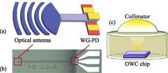
Figure 26. (a) Artist's impression of the IMOS-based OWC receiver. (b) Picture of the fabricated device. (c) Proposed receiver module with a micro-lens collimator assembled with the receiver chip [156].
Download figure:
Standard image High-resolution imageA first generation of the receiver has been fabricated, as depicted in figure 26(b). A uniform 10 × 10 µm2 SGC is utilized as the aperture for collecting light. The aperture size of the grating was chosen to match to the fiber-launched beam diameter used in a later system experiment. The >67 GHz UTC-PD (3 × 10 µm2) was employed as the light detection part. Details of the UTC-PD on IMOS can be found in section 5.2. The two parts are interconnected with a 400 nm wide single-mode InP waveguide. The receiver has been demonstrated in an OWC test bed with 2.4 km SMF and 2 m free pace propagation to simulate the indoor situation. Data transmission of 40 Gbit s−1 OOK signal at a single wavelength of around 1550 nm has been achieved, showing the high potential of this concept.
Since the device used an off-the-shelf grating coupler design, the field of view (FoV) was limited to about 7°–8°. Micro-lens collimators can be assembled into the receiver module to magnify the FoV, as illustrated in figure 26(c) [156]. The grating-based optical antennas are typically very flexible, thus can be engineered in the future work (e.g. by apodization [159] or controlled coupling [160]) to match to a specific far-field pattern determined by the OWC system. Metasurfaces have shown promising performances in terms of optical beam shaping, with much more compact form factors than conventional lenses [161, 162]. Recently Yulaev et al have reported the first on-chip metasurface integrated directly on top of waveguides and grating antennas, with simultaneous control over the emitting beam profile and the polarization [163]. This concept, so far demonstrated on Si, can be readily adapted to the InP membrane platforms due to their similarly high optical confinement and serves as a valuable BB for OWC antennas.
9.3. Light-based ranging and sensing
9.3.1. Non-contact ranging and sensing.
Light-based detection and ranging (LiDAR) has an enhanced resolution limit due to its shorter working wavelength compared to radio wave systems. There are several technological approaches for LiDAR, but the scanning LiDAR is widely believed to meet requirements of future self-driving cars. The core of a scanning LiDAR is an optical beam steerer, mainly by which the LiDAR resolution, refresh rate and detection range are determined. Due to the lack of a high-performance and low-cost optical beam steerer, commerical LiDAR nowadays are mostly bulky and expensive [164].
By leveraging the photonic integration technology, on-chip optical beam steerers can be realized, but their performance is still insufficient for real-life use. Beam steerers for automobile sensing should feature a detection distance of more than 200 m, a beam width of 0.1° or less, and a FoV of more than 90° [165]. To fufill these requirements, it is essential to have high optical output powers in the order of hundreds of mW and a large channel number in the order of 500. This results in a component count of more than 1000 on a single chip. Today's on-chip optical beam steerers are mainly made in InP-based [166] or Si-based material systems [165, 167–169]. However, neither Si nor conventional InP platforms provide out-of-the-box solutions for a fully-integrated high-performance optical beam steerer.
On one hand, with Si being a indirect bandgap material, it is still challenging to produce efficient gain on the native Si platform. Heterogeneous III–V integration does enables optical gain on Si, but efficient and compact active-passive coupling remains a challenge. The complex and hundreds-of-microns-long tapers [170, 171] will be a bottleneck for dense integration of actives. On the other hand, it is difficult for the conventional InP platform to integrate nearly 1000 components in one single chip, due to the large waveguide dimension and bend radii. Furthermore, considering the large component count, dense electrical interconnection for control circuits will be challenging on both platforms.
InP membrane technology can tackle these challenges by providing active-passive integration together with sub-micron highly confined waveguides. Both efficient gain and dense circuits can be realized in a single membrane layer. Dense electrical interconnects can be realized with through polymer vias (TPV, see section 8.1), which can potentially integrate the InP beam steerer with the control circuits in one chip.
Recently, Wang et al have demonstrated a grating antenna BB for beam steering on the IMOS platform [172], which exhibited a beam width of 0.05°, setting a record for InP-based beam steerers. The antenna features a fabrication insensitive design and utilizes the double-sided processing for performance boost. By tuning the wavelength of the input light, the beam can be steered in one dimension. The other dimension can be tuned by forming a 1D phased array. The characterization of a fabricated standalone antenna is shown in figure 27. The length of the grating is 2 mm. The measured angular beam width is 0.05°, which set a record for InP-based optical beam steerers. A FoV of 14°, which corresponds to a spatial resolution of 280, has been achieved by tuning the input wavelength over 110 nm. Integrated metalenses can be used to further increase the FoV. This BB contributes crucially towards a fully integrated high resolution beam steerer on InP membrane photonics.
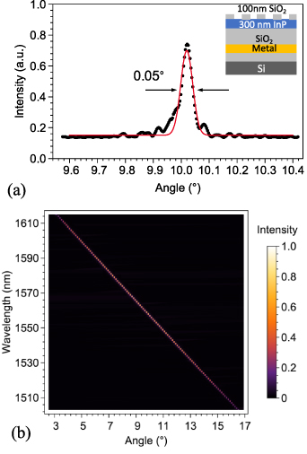
Figure 27. Measured far-field pattern of a 2 mm long grating antenna on IMOS [172]. (a) far-field beam profile (dotted) and gaussian fit (red line). Inset: schematic illustration of the grating antenna. (b) Steering map of the grating antenna by tuning the input wavelength.
Download figure:
Standard image High-resolution image9.3.2. Displacement sensing.
IMOS platform is also promising for contact sensing applications such as displacement sensing for atomic force microscopy, using the integrated NOEMS technology (see section 3.6). A four-core coupled waveguide scheme has been proposed and demonstrated [173] for the displacement sensing. Unlike conventional approaches using resonant structures, this scheme takes advantage of the high sensitivity of the propagation constants of the supermodes to the change of the coupling condition (e.g. a slight displacement of one of the waveguides). The fabricated device and it is working principle are shown in figure 28. The sensor has a state-of-the-art sensing accuracy at fm Hz−1/2 level and a record wide optical bandwidth of 80 nm, thanks to its non-resonant nature.
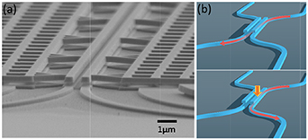
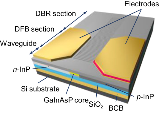
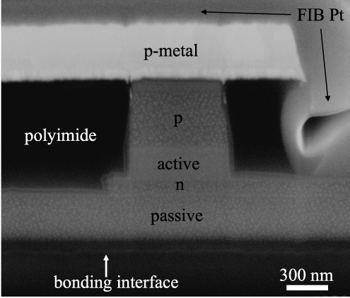
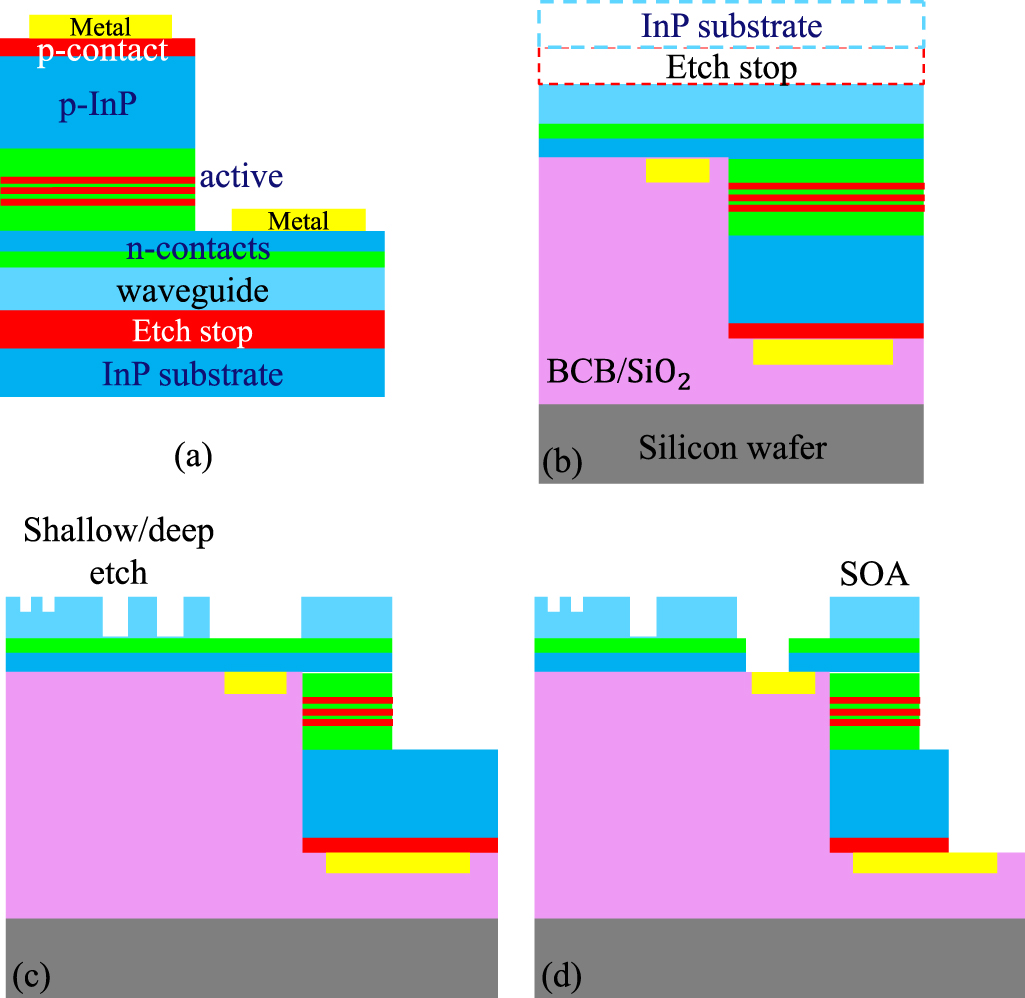
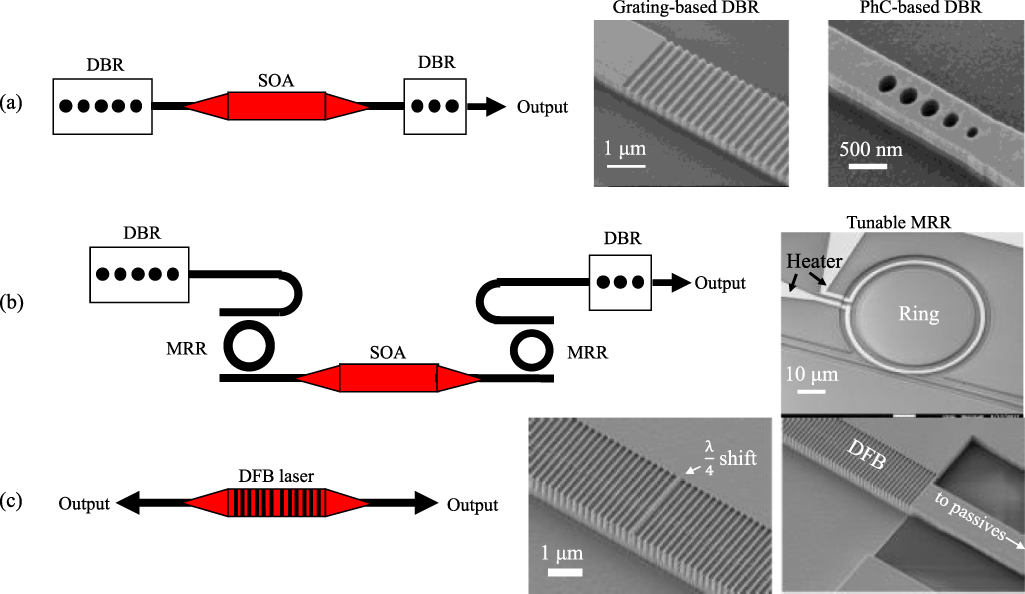
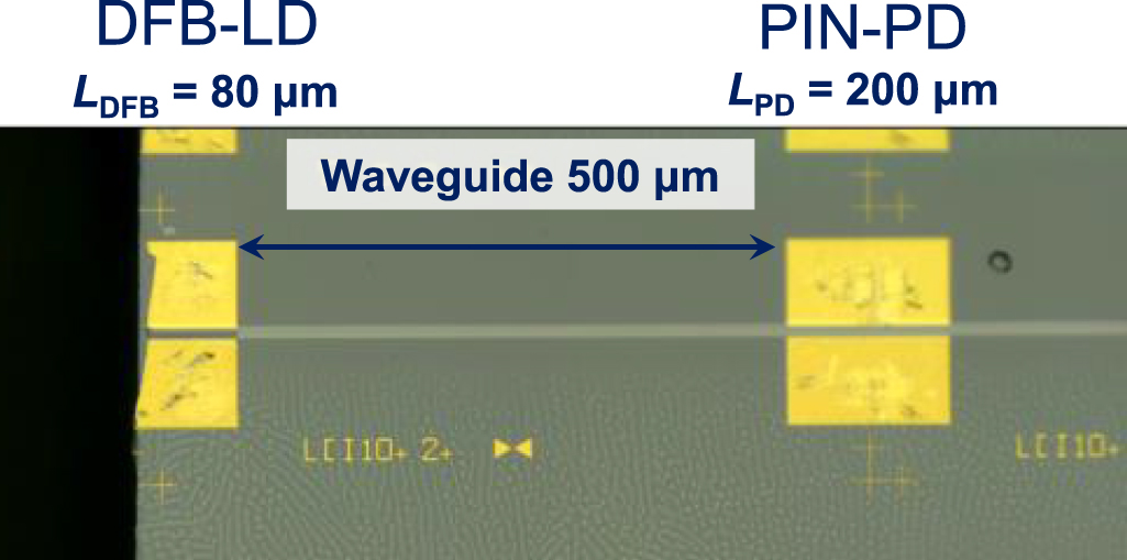
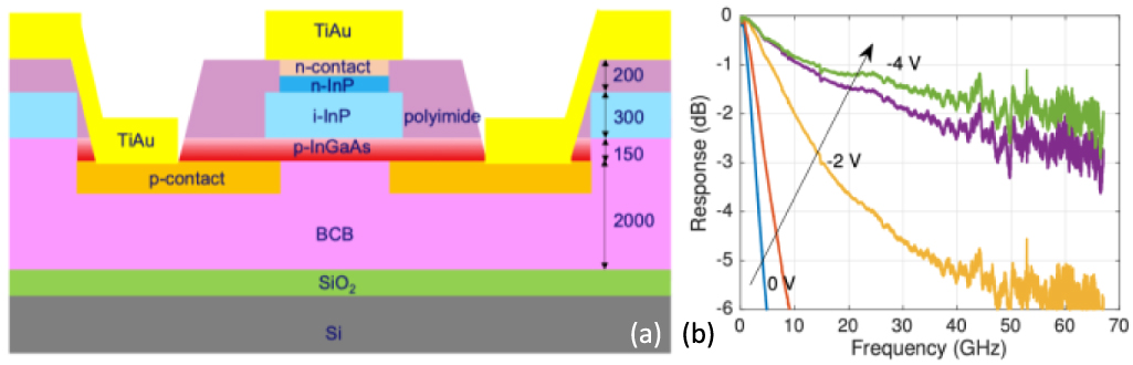
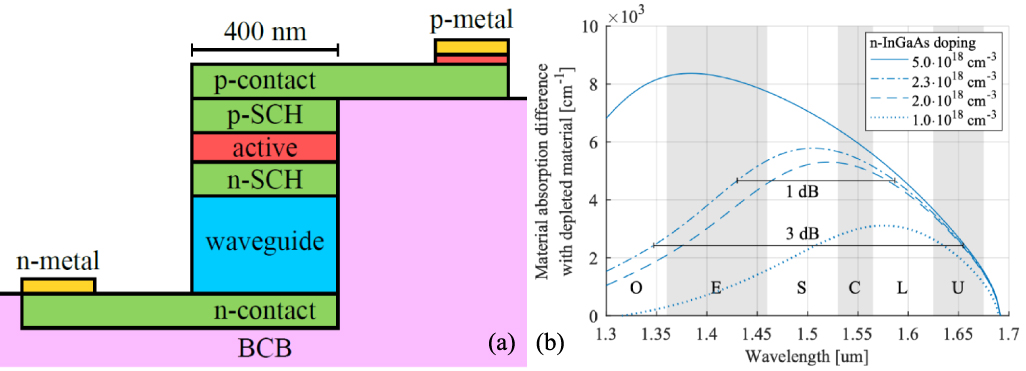
Figure 28. (a) Picture of the fabricated NEOMS displacement sensor on IMOS platform. (b) Schematic illustration of the working principle [173].
Download figure:
Standard image High-resolution image
More interestingly, the displacement sensor is equipped with on-chip photodiodes for direct readout. The photodiodes and the sensor share a membrane layer stack which is very similar to the compact twin-guide SOA described in section 2.2.2. This will enable future fully integrated optomechanical sensors, removing the need of bulky free-space sources and detectors.
10. Conclusion
The photonic integration on a thin membrane composed of InP and its III–V compounds is a relatively new research domain. It combines several features from different existing photonic integration platforms; on one hand it offers intrinsic active-passive integration; on the other hand it offers sub-micron sized nanophotonic circuitry. It has high potential to miniaturize active devices and break the bottleneck of integration density. This field, pursued by several research groups globally, has resulted in highly versatile technology platforms, which are reviewed in this paper.
The lateral diode scheme aims for the highest laser efficiency for the application domain of optical interconnects. The extremely thin (∼300 nm) and short (<50 µm) membrane lasers have achieved <100 fJ bit−1 energy efficiency at 20 Gbps, while at the same time they enable monolihtic integrated optical interconnect links with passive waveguides and photodiodes based on the butt-joint regrowth technology.
The vertical diode scheme focuses on generic integration using regrowth-free twin-guide integration for complete functionality. A wide variety of lasers can be constructed by combining the highly efficient amplifier BB with nanophotonic passive components. The double-sided processing technology also enables the integration of highly different layer stacks (e.g. for an ultrafast UTC photodiode or for a wideband band-filling modulators) in the membrane.
Co-integraiton with electronics will maximize the speed and energy advantages in InP membranes. The heterogeneous integration approach can combine mature foundry produced wafers and co-integrate them in a post-processing step. Least performance compromises in photonics and electronics can be achieved with coordinated co-designs. The monolithic approach, on the other hand, can achieve photonic and electronic components using a single combined process flow. The wafer size mismatch in the heterogeneous approach is thereby solved. However, it will be challenging to manage the impact of the combined flow on device performances.
Finally, similar to the path of the generic InP and silicon photonics platforms, the InP membrane (the IMOS platform) has now moved to wafer-scale processes and initiated the development of a process design kit, both of which will pave the way towards an open access of the fully integrated nanophotonic platform to a wide range of optical designers.
Acknowledgments
The authors from TU/e acknowledge the Dutch NWO Zwaartekracht Grant Research Center for Integrated Nanophotonics, the ERC Proof-of-Concept Grant IMOS4ALL and the EU H2020 projects WIPE and TWILIGHT. The use of the cleanroom facilities at the Nanolab@TU/e is acknowledged.
The works of the authors from Tokyo Tech are supported by Japan Society for the promotion of science (JSPS) KAKENHI.