

Abstract
In this work, a path to overcome the highest current efficiency on SnS thin-film solar cells by the Se incorporation is presented. We carried out a theoretical study of the effect of different Se/(S + Se) compositional ratios (CRs) (from 0.0 to 1.0) on the solar cell performance. In this sense, an improvement on power conversion efficiency (PCE) by decreasing the energy band gap (theoretical Se incorporation) from 1.35 to 1.08 eV was observed. All electrical output parameters (open-circuit voltage, short-circuit current density, fill factor and PCE) were increased by an augment of the CR from 0.25 to 0.75. A PCE of 10.23% was obtained for a CR of 0.75. Furthermore, a thickness optimization of the absorber was carried out, where the greatest PCE of 11.78% was obtained at 800 nm. On the other hand, a simulation at different work functions in back contact and different bulk defect density on the absorber were performed in order to achieve higher efficiencies.
Export citation and abstract BibTeX RIS
List of symbols
| Eg | Energy band gap (eV) |
| χ | Electron affinity (eV) |
| J | Current density (mA cm−2) |
| V | Voltage (V) |
| PCE | Power conversion efficiency (%) |
| Jsc | Short-circuit current density (mA cm−2) |
| Voc | Open-circuit voltage (V) |
| FF | Fill factor (%) |
| Ec | Conduction band energy |
| CB | Conduction band |
| VB | Valence band |
| ND | Donor density (cm−3) |
| NA | Acceptor density (cm−3) |

| Relative dielectric permittivity |
| Nt | Defect density (cm−3) |
| α | Absorption coefficient (cm−1) |
| CR | Compositional ratio |
| d | Thickness (nm) |

| Electron mobility (cm2 Vs−1) |

| Hole mobility (cm2 Vs−1) |
1. Introduction
Solar cells based on CIGS and CdTe technologies use absorber materials that have the disadvantage of containing scarce and toxic elements. For this reason, different types of materials for thin solar cells with adequate physical properties are investigated. Among the absorber materials are the kesterites. The power conversion efficiency (PCE) of the CZTS and CZTSe based thin film solar cells has been improved. Until now, a PCE of 9.2% and 11.6% for CZTS and CZTSe has been demonstrated, respectively [1, 2]. The highest PCE of 12.6% was achieved by Se-rich CZTSSe thin film solar cells with a S/(S + Se) compositional ratios (CR) of 0.24 [3]. Other materials of interest are binary sulfides, which have a simpler composition than kesterites. The SnS (Tin sulphide) has adequate properties for photovoltaic applications and could be the future of energy source due to its abundance and non-toxicity with optimal energy band gap of ≈1.35 eV [4]. This semiconductor material is in the group IV–VI compound with an orthorhombic crystal structure, with absorption coefficient of (104cm−1) and a high carrier concentration of (1015, 1018 cm−3). Moreover, a study has reported theoretical PCEs > 30% for solar cells with absorber with Eg of 1.1–1.4 eV [5], therefore, greater efficiencies can be expected for SnS solar cells. On the other hand, the S substitution by Se to obtain SnSe solar cells in order to achieve better efficiencies has been study. Several reports show a low band gap around 1.0 eV for SnSe because the Se influence, which is similar to the kesterite (CZTSe) [6]. Furthermore, both solar cells with SnS and SnSe are widely studied as an absorber material. However, the maximum efficiencies experimentally reported for these material based-devices are 4.36% and 6.44%, respectively [7, 8]. Several studies of solar cells with kesterite such CZTSSe have shown an improvement in morphological, structural, optical (tunable band gap from 1.5 eV to 1 eV) and electrical properties by the incorporation of Se [9–12]. This enhancement implied a significant efficiency performance in the solar device with a record as it was mentioned above with a band gap (CZTSSe) of 1.13 eV [3]. Nevertheless, some experimental studies have been reported on ternary materials of the SnS2(1-x)Se2x and 2D SnSe2(1-x)S2x type, for application in devices such as photodetectors and phototransistors [13, 14]; and there are few studies of the application of SnSxSe1-x in solar cells, which have too low efficiencies [15, 16]. On the other hand, there are no simulation and optimization studies of these devices, nor the device with the highest current efficiency [7]. In this paper, a numerical modeling was carried out by SCAPS, which is a solar cell simulator widely used for other materials such perovskite, CdTe, CIGS, kesterites, etc [12, 17–19]. Our work presents a theoretical study, which is reported for the first time, about the effect of Se incorporation in the performance of solar cells with SnS as absorber material in order to enhance the performance of the SnSSe solar cell.
2. Theoretical details
2.1. Device configuration
Researchers have currently shown great interest in numerical simulation to study and design materials of solar cell. In our proposed model, the p-type SnS is used as absorber layer in the solar cell simulation. The solar cell configuration was based on the current record device [7], where some of their results and material properties were taking into account as reference for our model. The band gap and electron affinity of this layer were varied in order to obtain SnSSe and evaluate the Se composition on the device performance. The schematic view of the proposed solar cell structure is shown in figure 1(a), where a multilayer planar structured solar cell with thickness values of ITO (300 nm), ZnO (10 nm), Zn(O,S):N (30 nm), SnO2 (1 nm), SnSSe (500 nm) and Mo (450 nm) was simulated numerically using SCAPS-1D device simulation software. Im et al reported that the CB can be modified by the Se incorporation, while the VB still constant [20]. In figure 1(b) is presented a band energy diagram of Zn(O,S) buffer layer, and the five absorber layers (SnSxSe1-x with different Se/(S+Se) CRs) that we used for our simulations (see references in section 2.3).

Figure 1. (a) Device configuration used in SCAPS for SnSSe solar cell simulation, (b) band energy diagram of Zn(O,S) buffer layer and SnSSe absorber layers with different Se/(S + Se) CRs.
Download figure:
Standard image High-resolution image2.2. Simulation model
Several works have demonstrated the importance of numerical modeling for enhancing the performance of thin-film solar cells, by solving the basic equations of semiconductors, as well as, helping to understand and predict the impacts for each material layer of a solar cell [21–23]. The simulations in this work were carried out by SCAPS-1D, under standard conditions; AM 1.5 solar spectrum at room temperature (300 K). This program resolves three differential equations for J-V characteristics (Poisson, continuity and drift diffusion) at each position throughout the solar cell by taking into account the boundary conditions [24]. Furthermore, the software simulates the device performance by considering the Shockley-Read-Hall recombination.
Poisson equation,
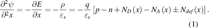
This equation relates the electric field  of p-n junction to the space charge density
  . Where,
  is the electrostatic potential,
  is the static material's permittivity,
  the elementary charge (1.6 × 10⁻¹⁹ C),
  the hole density and
  the electron density. Finally,
  and
and  are ionized donor and acceptor densities, respectively.
Electron and hole, carrier continuity equations at steady state,
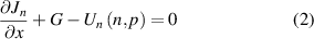
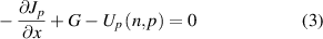
where  ,
,  are current density of electron and hole carriers,
  ,
,  are the net recombination rates and
  is the electron-hole generation rate.
Drift diffusion (total current density) equations,
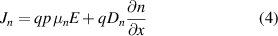
where  ,
,  are the electron and hole mobility carrier,
  is the elementary charge, and
  ,
,  are the diffusion coefficients of electron and hole, respectively.
2.3. Device parameters
Material properties are summarized for each layer in table 1. These data were obtained from the literature [4, 7, 21, 25–31]. In the present study, the device parameters such as thickness of active layer were optimized using the SCAPS-1D simulator. Work functions used were 4.4 eV for ITO as front contact and 5.0 eV for Mo as back contact [21] with surface recombination velocity of 1 × 105 cm−1 and 1 ×107cm−1 for electrons and holes, respectively. In the present work, it is assumed that there is no presence of secondary phases in SnSxSe1–x absorber, which has been experimentally demonstrated by deposit control [32]. It should be noted that by implementing a compositional change of the SnSxSe1–x absorber layer, not only the band gap ( , but almost all other materials properties including electron affinity (χ), optical absorption, doping density, transport properties and recombination properties are varied according with the Se contents in the absorber. Nevertheless, in this work, only the
  and χ values from the SnSxSe1-x layer was varied as function of the Se content (x), while the other properties are considered constant. This last assumption is due to the scarce of material properties in the literature about the SnSxSe1-x thin film. However, Walsh et al has demonstrated that in kesterite,
  decreases almost linear by the Se incorporation from 1.5 eV (CZTS) to 1 eV (CZTSe) [33]. Theoretical and experimental studies have been reported a non-linear behavior of Eg with the composition in SnS2(1-x)Se2x alloys [14, 34]. However, for the SnSxSe1-x material have been reported a linear behavior with the increasing of Se content, where the optical bowing parameter (b) is very small [35], and even can be considered as zero [36]. Hence, it can be assumed that for SnSSe as well as the kesterites, the band gap (
 ) decreases from 1.35 eV at
  to 1 eV at
  , with a small bowing parameter reported in equation (6) (Vegard´s law). In this work is considered b = 0 and as consequence, a linear dependence of the Eg. as function of
  . According to this behavior, the
  and χ of SnSxSe1-x at different Se concentration are determined by:


Table 1. Material layer parameters of the SnSSe solar cell.
| Parameters | ITO | ZnO | Zn(O,S):N | SnO2 | SnS (reference device) | SnSSe |
|---|---|---|---|---|---|---|
| d (nm) | 300 | 10 | 30 | 1 | 500 | 500 |
| Eg (eV) | 3.65 | 3.4 | 2.7 | 3.6 | 1.35 | Variable |
 (eV) (eV) | 4.8 | 4.6 | 4.3 | 4.5 | 3.9 | Variable |

| 8.9 | 9 | 10 | 9 | 12.5 | 12.5 |

| 10 | 100 | 4.7 | 100 | 100 | 100 |

| 10 | 25 | 1 | 25 | 4 | 4 |

| 2 × 10¹⁹ | 1017 | 9.3 × 10¹⁶ | 1020 | 0 | 0 |

| 0 | 0 | 0 | 0 | 5.7 × 10¹⁵ | 5.7 × 10¹⁵ |
| α (cm−1) | 106 | Data file | 105 | 105 | 104 | 104 |
| Nt (cm−3) | Data file | Data file | — | — | 1015 | 1015 |
As shown in figure 1(b), the Eg and χ change depending on the composition. These values are:
Eg = 1.35, 1.26, 1.17, 1.08 1.0 eV and  = 3.9, 3.98, 4.07, 4.15, 4.23 eV.
3. Results and discussion
3.1. Numerical simulation of reference SnS solar cell
As a starting point, the modeling of SnS solar cell (structure shown in figure 1(a)) was performed by SCAPS. Figures 2(a) (J-V curve) and (b) EQE shows the results of the theoretical simulation. A good approximation with the experimental parameters of record solar cell (Sinsermsuksakul et al) is observed.

Figure 2. Numerical simulation of the SnS solar cell. (a) Output parameters and (b) external quantum efficiency.
Download figure:
Standard image High-resolution image3.2.
SnSSe devices with different
 CRs
CRs

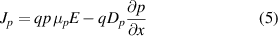
Within the scheme of figure 1(b), was observed that the energy band gap (Eg) and electron affinity (χ) of the SnS layer can be tailored by the Se incorporation. As the Eg and χ of window layer and SnS thin film have different values, there are discontinuity in conduction band and valence band of the window/SnS interfaces. The Se addition modifies the conduction band offset ΔEc and, as a consequence, the properties of the window layer/SnS heterojunction. Therefore, the effect of the incorporation of Se on the output parameters of the SnS solar cell is shown in figure 3. Furthermore, the output parameters are summarized in table 2.
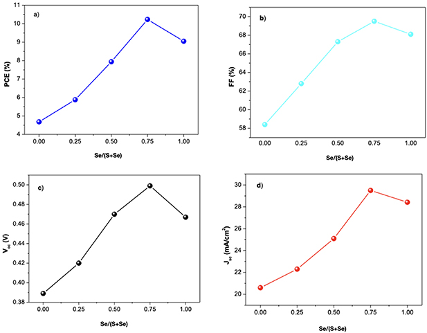
Figure 3. The effect of different Se/(S + Se) CRs on SnS solar cells: (a) PCE, (b) fill factor (FF), (c) open-circuit voltage (Voc) and (d) short-circuit current density (Jsc).
Download figure:
Standard image High-resolution imageTable 2. Theoretical output parameters of SnS solar cell at different Se/(S + Se) CRs.
| Se/(S + Se) | Eg (eV) | Voc (V) | Jsc (mA cm−2) | FF (%) | PCE (%) |
|---|---|---|---|---|---|
| 0.0 | 1.35 | 0.389 | 20.6 | 58.4 | 4.68 |
| 0.25 | 1.25 | 0.42 | 22.3 | 62.8 | 5.88 |
| 0.50 | 1.18 | 0.47 | 25.1 | 67.3 | 7.94 |
| 0.75 | 1.07 | 0.499 | 29.5 | 69.5 | 10.23 |
| 1.0 | 1.0 | 0.467 | 28.48 | 68.1 | 9.05 |
In figure 3 is observed that the SnS solar cell performance depends on the Se incorporation. All output parameters (Voc, Jsc, FF and PCE) increased by increasing the CR from 0.0 to 0.75 and decreased at a CR = 1. The figure 3(a) shows that the greatest PCE was achieved at 0.75 CR with a 10.23% value. This implies an increase of 2.35 times compared with the SnS solar cell without Se. Figure 3(b) presents the same behavior on the FF reaching a 69.5% for a CR of 0.75. The figure 3(c) presents as well an increase of Voc with the Se incorporation, where a 0.499 V was obtained at 0.75 CR. However, the Voc was reduced to 1.0 CR. The improvement of Voc indicates a greater separation of fermi quasi levels, which could be attributed to a greater radiation absorption and efficient transfer of electron photogenerated in the absorber. Moreover, the Jsc values are observed in figure 3(d). The greatest value was achieved at 0.75 CR with 29.5 mA cm−2. The increasement of Jsc by Se incorporation could be due to an absorption improvement by decreasing the Eg (from 1.35 to 1.08 eV), which extended the absorption range at greater wavelength as was observed in EQE (figure 4). The reduction of FF, Voc and Jsc at 1.0 CR could be attributed to a large barrier at the absorber/buffer layer interface, which affects the transfer of electrons from the absorber to the external circuit. A more detailed discussion of these issues is done below (see discussion of figure 5).
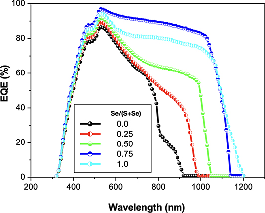
Figure 4. Theoretical external quantum efficiency of SnS solar cells at different Se/(S + Se) CRs.
Download figure:
Standard image High-resolution image
Figure 5. Energy band diagram of the heterojunctions: (a) Zn(O,S)/SnSe and (b) Zn(O,S)/SnS.
Download figure:
Standard image High-resolution imageIn figure 4 is presented the EQE for solar cells at different Se/(S + Se) CRs (0.0, 0.25, 0.50, 0.75 and 1.0). It is observed that when the CR increases, the EQE response expands towards greater wavelengths, which corresponds to the decrease of the band gap (from Eg = 1.35 eV (for CR = 0.0) to Eg = 1.0 eV (for CR = 1.0)). It is also observed that the EQE increases in the whole wavelength spectrum, when the CR is increased from 0.0 to 0.75, which could be owing to the fact a greater absorption of the incident radiation. However, the EQE of the solar cell with CR = 1.0 (SnSe) was slightly decreased, which could be because of resistive effects that affect the transport and collection of charge carrier. The results of figure 4 are in good correspondence with the behavior shown in figure 3(d).
The behavior shown in figures 3 and 4 could be explained, based on the understanding that changes in CR produces modifications in the band gap of materials and in the band alignment of heterojunctions. These modifications, impact on processes of radiation absorption, recombination, transport and collection of charge carriers. This scheme has been observed in Zn(O,S)/SnS [6, 37] and other heterojunctions [38–40]. In the present work, the increment of Se/(S + Se) CR produces a reduction of the minimum of the conduction band and the energy band gap of the absorber. The reduction of the minimum of the conduction band generates band alignment changes, which impacts on processes of recombination, transport and collection of charge carriers. The reduction of the energy band gap has an impact on the absorption. In figure 5 are presented the opposite CR cases, SnSe and SnS. Figure 5(a) shows the SnSe as absorber. In this case, the energy band gap is the lowest, which improves the absorption. However, the reduction of the minimum conduction band generates an increment on conduction band offset (ΔEc). This behavior, implies the presence of a large barrier at Zn(O,S)/SnSe interface that affects the output of electrons from the absorber to the Zn(O,S) buffer layer, and to external electrical circuit. Hence is reflected in a reduction of FF, Jsc and Voc. This corresponds to that reported by other authors [37], according to which the increase in the barrier at the SnS/Zn(O,S) interface (due to compositional changes in the Zn(O,S) buffer layer) affects the FF, Jsc and Voc of the cells. On the other hand, figure 5(b) presents the case of the solar cell with SnS as absorber. The SnS has the highest energy band gap and conduction band minimum. In this case, the conduction band offset (ΔEc) is positive but low, which implies the presence of a small barrier at Zn(O,S)/SnS interface. So, allows the output of electrons from the absorber to the external electrical circuit. Besides, the Jsc is affected by the relative wide energy band gap of the absorber. The opposite analyzed cases (SnSe and SnS) show that a wide energy band gap (SnS case). This implies a minimal barrier to the transport of photogenerated electrons in the absorber, but a poor absorption; while a narrow energy band gap (SnSe case) implies better absorption. Nevertheless, the presence of a high barrier affects the transport. The above explains why a SnSSe structure (with a CR = 0.75) has a better performance as were shown in results above.
3.3. Device optimization
3.3.1. Thickness optimization.
Is well known that the absorber thickness has an influence in the device performance. In this section, the influence of the SnSSe thickness (with CR = 0.75) on the solar cell has been studied. This effect is shown in figure 6 and in table 3 the output parameters are presented.
Figure 6. Theoretical effect of the absorber thickness on SnSSe solar cell performance.
Download figure:
Standard image High-resolution imageTable 3. Output parameters of SnSSe solar cell as function of absorber thickness.
| Thickness (nm) | Voc (V) | Jsc (mA cm−2) | FF (%) | PCE (%) |
|---|---|---|---|---|
| 100 | 0.359 | 18.37 | 56.1 | 3.69 |
| 200 | 0.42 | 21.2 | 62.5 | 5.56 |
| 300 | 0.486 | 26.8 | 66.3 | 8.63 |
| 400 | 0.495 | 28.9 | 68.7 | 9.82 |
| 500 | 0.499 | 29.5 | 69.5 | 10.23 |
| 600 | 0.52 | 29.99 | 70.43 | 10.98 |
| 700 | 0.528 | 30.36 | 70.81 | 11.35 |
| 800 | 0.537 | 30.797 | 71.28 | 11.78 |
| 900 | 0.537 | 30.54 | 71.05 | 11.65 |
| 1000 | 0.537 | 30.28 | 70.79 | 11.51 |
The thickness of the absorber was varied over a wide range (from 100 to 1000 nm). In figure 6 and table 3 it is observed that the Voc experiences a significant increase with increasing thickness of the absorber, going from 0.359 V (for 100 nm) to 0.537 V (for 800 nm). The Voc is kept constant for higher thicknesses. For its part, the Jsc increases by the increment of the absorber thickness (which could be due to a greater radiation absorption), reaches a maximum of 30.797 mA cm−2 for a thickness of 800 nm, and decreases slightly for greater thicknesses (which corresponds to the fact that an excessively thick absorber affects the carriers transport and collection). The FF shows a behavior similar to the Jsc. The PCE, on the other hand, increases with the increment of the absorber thickness, reaching a maximum for 800 nm, and decreases slightly for greater. With a thickness of 200 nm of the ternary absorber (CR = 0.75), an efficiency of 5.56% is obtained. This value is superior to the record efficiency of the SnS solar cell (4.36%), obtained with a thickness of 500 nm of the binary absorber material. It is observed, thus, that ternary material enhances the use of thinner films in solar cells. With 500 nm of ternary absorber (SnSSe) at CR = 0.75, an efficiency of 10.23% was obtained (which is more than double the record efficiency mentioned above). The greatest PCE is 11.78% and was achieved for an absorber thickness of 800 nm. This PCE means an increase of 2.7 times with respect to the record efficiency of the SnS solar cell. The previous results show that the use of SnSxSe1-x ternary type as an absorber material constitutes a very interesting way to increase the efficiency of solar cells with respect to binary type absorber (SnS).
3.3.2. Work function in back contact.
There are two types of metal-semiconductor contacts: the rectifying and the nonrectifying or ohmic types. In the contact rectifier, there is a potential barrier that affect the charge carrier collection. On contrary, an ohmic contact has a negligible contact resistance relative to the bulk or series resistance of the semiconductor, thus an enhancement on internal collection processes on the solar cell is produced. There are several reports about the work function (WF) of the contacts (back and front), which has an influence on these processes [17, 41, 42]. For SnS solar cell, the record efficiency was obtained by using Mo (5.0 eV) as back contact. In this work, we varied the WF of the back contact from 4.7 to 5.7 eV in order to study this influence on the output parameters of solar cell (with a CR = 0.75 and an absorber thickness of 800 nm). In figure 7 is shown the effect of different WF of back contact on SnSSe solar cell performance.
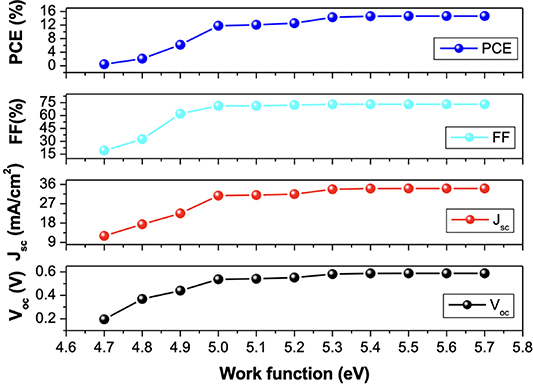
Figure 7. Theoretical study of the effect on different WF (back contact) on the SnSSe solar cell performance.
Download figure:
Standard image High-resolution imageIn figure 7 is observed that all electrical parameters increase with increasing the WF. This suggests the formation of a less resistive contact (a barrier reduction) and greater carrier collection. It is observed that the maximum PCE (14.65%) was obtained for a value of 5.4 eV and keeping constant for higher values. However, a decrease on the efficiency for lower WF values was perceived. The observed behavior reveals the importance of finding new materials with greater WFs than Mo for this type of device.
3.3.3. Bulk defect density on the absorber.
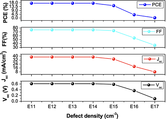
The defect in bulk material usually act as recombination (Shockley-Read-Hall non-radiative) centers for photo-generated carriers, resulting in the decrease of the FF, Jsc and Voc. In this sense, a simulation under different defect densities (1011–1017 cm−3) was carried out in order to evaluate the impact of the defect density on the SnSxSe1-x solar cell performance. For this study was employed the device with the greatest PCE (14.65%), which has a defect density of 1015 cm−3. This effect is presented in figure 8.
Figure 8. Theoretical effect of the absorber (CR = 0.75) defect density (Nt) on the solar cell performance.
Download figure:
Standard image High-resolution image
Figure 8 shows the effect of bulk absorber defect density on solar cell performance. It is observed that the Jsc, FF, Voc and PCE of the solar cells show a stable behavior, with relatively high values, for a defect density between 1011 and 1014 cm−3. The performance of the devices is observed to get worse for Nt ≥ 1015 cm−3. The greatest efficiency was 17.56% at 1014cm−3 of bulk defect density, while the lowest was of 0.26% for defect density of 1017 cm−3. The previous results indicate, on the one hand, that the performance of these devices has a certain tolerance to the defects of the absorber layer. On the other hand, in order to obtain high efficiencies, these defects must not exceed the critical value (∼1014 cm−3).
4. Conclusion
In the present study, a numerical simulation of a SnS-based solar cell was performed using SCAPS-1D. In order to promote strategies to overcome the best record SnS solar cell of 4.36%, a theoretical study of the effect of Se incorporation was carried out (using the same SnS solar cell structure). In this proposal, we varied some optical properties such Eg and χ of the SnS absorber layer, which mainly represent the effect of different Se/(S + Se) CRs to form the SnSSe solar cells. The greatest PCE (10.23%) was obtained for a CR of 0.75. Moreover, an optimization thickness of the SnSxSe1-x absorber was carried out, where the greatest efficiency (11.78%) was obtained for a thickness of 800 nm. In addition, the WF on back contact was evaluated. Here, we achieved in our theoretical modeling the greatest PCE of 14.65% for WF >5.4 eV. Furthermore, a study of the effect of bulk defect density (Nt) on the absorber was carried out. In this last study, a PCE of 17.56% was obtained at Nt of 1014 cm−3. Although, more efforts in new SnS solar cell structures need to be studied, the present work shows a considerable enhancement on efficiency by using SnSSe instead of SnS as an absorber layer.
Acknowledgments
Authors wish to thank Dr. Marc Burgelman from University of Gent for providing SCAPS software.