

Abstract
Metamorphic InAs/InGaAs quantum dots (QDs) have been proposed as active elements for optoelectronic light-emitting devices operating in the infrared range. However, advanced structure design to allow efficient and stable enhancement of quantum yield at room temperature are still needed. Here, we compare a metamorphic InAs/In0.15Ga0.85As QD heterostructure with and without GaAs confining barriers, to investigate the effect of introducing GaAs barriers on the photo- and thermo-electrical properties. GaAs confining barriers allow to enhance the QD photoluminescence intensity at 1.3 µm, i.e. second telecommunication window, by more than two orders of magnitude at room temperature and at 80 K. We also discuss the effect of GaAs barriers on the carrier transport and on defect-related levels detected by means of photocurrent and deep level thermally stimulated current spectroscopies. GaAs confining barriers decrease the thermal escape rate of electrons confined in QD and wetting layer, thereby highly increasing the radiative recombination and also quenching the photocurrent. At low temperatures, the barriers also reduce the capture of electrons generated in InGaAs by the QD layer and, on the other hand, prevent the trapping of electrons outside the QD layer, decreasing carrier lifetimes. The deep levels identified as point and extended defects have been detected in the InGaAs layers. There are no new types of defects introduced in the structure by the addition of the barriers, but this causes a weakly increased density of traps near QDs. Our results show that InAs/InGaAs QDs with GaAs confining barriers can be efficient light emitters with only a slight increase of defects in the structure. Hence, such advanced design for metamorphic QDs can be of relevant interest for applications in energy-efficient QD lasers, optical amplifiers and single-photon emitters operating at 1.3–1.55 µm.
Export citation and abstract BibTeX RIS
1. Introduction
Semiconductor In(Ga)As/(In)GaAs nanostructures are widely used in optoelectronics as infrared (IR) light detectors [1, 2], cameras [3, 4], and solar cells [5–7]. However, the most productive applications of these nanostructures are IR light-emitting devices, such as energy-efficient lasers [8, 9], single-photon emitters [10, 11], quantum dot (QD) optical amplifiers [1], etc. Metamorphic nanostructures with InAs QDs embedded in InGaAs metamorphic buffer (MB) are a development of standard InAs/GaAs structures that allow increase of the emission efficiency and enhance the range deeper into the IR range reaching the second and third telecommunication windows at 1.3 and 1.55 μm, respectively [12–14]. Such an improvement is due to less lattice mismatch between In(Ga)As QDs and InGaAs MB, leading to lower strains in the QDs. On the one hand, this causes narrower bandgap of the nanostructures, which, hence, reduces the emission energy [13, 15]. On the other hand, the lower strains in QDs and MB mean a lower amount of lattice defects in the environment of nanostructures and, in turn, lower non-radiative recombination [16]. We have recently shown that the efficiencies per one QD are similar for both conventional InAs/GaAs and InAs/In0.15Ga0.85As QD structures [17].
However, metamorphic InAs/InxGa1–xAs QD structures reveal some other types of defects compared to InAs/GaAs ones [18–20], and an increase in In content x, being necessary to redshift emission towards 1.55 μm, increases the amount of defect-related states in the structure, causing a reduction of luminescence efficiency [16]. Furthermore, the application of InGaAs containing layer instead of GaAs lowers the potential barrier for the charge carriers confined in QDs to escape, resulting in an enhanced emission quenching.
To achieve a better emission efficiency, additional layers of wider-gap materials were suggested to be grown on both sides of the InAs QD layer. The wide-gap barrier layers would improve the quantum confinement of charge carriers and limit their escape from the nanostructures [14, 21, 22]. The studies have shown that the use of thin GaAs and InAlAs confining barriers (CBs) indeed increases the photoluminescence (PL) yield significantly, shifting herewith the spectrum toward higher energies due to the better quantum confinement of charge carriers. Thus, the barrier-equipped metamorphic QD (QD-CB) structures are successfully approached to enhance efficiency of light-emitting devices.
However, the topic of lattice defects and related energy levels due to the addition of CBs remains still unexplored. Indeed, InGaAs/GaAs interface is known to be an origin of numerous extended defects (EDs), such as threading and misfit dislocations [20] propagating, respectively, across and along the interface in the structure grown by molecular beam epitaxy (MBE). Meanwhile, the understanding of defect spectrum and their influence on the structure properties is always desirable for device applications. As we have recently shown [18, 19], the defect traps can sufficiently affect PL and photoelectric properties of InAs/InGaAs QD structures.
In this work, an InAs/In0.15Ga0.85As QD heterostructure with 6 nm GaAs barriers confining the InAs QD layer from both sides is studied by luminescent and photoelectric spectroscopies in comparison with a similar structure without CBs. The barrier-free metamorphic structure grown at certain design does not demonstrate any detectable PL at room temperature. The addition of CBs allows to enable room temperature QD PL and to enhance the low-temperature emission by more than two orders of magnitude. Here we also focus on an in-detail investigation of carrier transport and defect-related deep levels by means of dc photocurrent (PC) and thermally stimulated current (TSC) transient spectroscopies.
2. Methods
2.1. Sample preparation and description
The studied undoped InAs/In0.15Ga0.85As QD structures were grown on semi-insulating GaAs (100) substrates with resistivity of 108 Ω × cm in an MBE chamber under UHV. Initially, a 100 nm thick GaAs buffer was deposited by MBE at 600 °C. The rest of the structure was grown by atomic layer MBE (an MBE variant where molecular fluxed imping alternatively on the growing surface), while GaAs CBs were grown by conventional MBE. An In0.15Ga0.85As MB layer was grown at 490 °C. Thereafter, a 21 MLs (monolayers) thick (about 6 nm) GaAs lower barrier (LB) was deposited by MBE at the same temperature and, then, covered by a 4 MLs (about 1 nm) thick In0.15Ga0.85As smoothing layer (SL) to avoid differences in surfaces overgrown by QDs. Indeed, it has been discussed how the chemical composition of the surface on which QDs grow has in impact on the critical thickness for three-dimensional growth of InAs islands [23]. Then, the temperature was lowered to 460 °C to deposit 3 MLs of InAs. After a growth interruption of 210 s for cooling the sample to 360 °C, the 21 MLs GaAs upper barrier (UB) followed by an In0.15Ga0.85As cap as the upper cladding layer were grown.
For comparison, a pristine InAs/In0.15Ga0.85As QD structure without GaAs CBs was grown under the same growth conditions. In any case, the thickness of the total lower cladding layer, including LB and SL in the structure with CBs, was 60 nm, whereas the upper cladding layer (together with UB in the respective sample) was 20 nm thick. The InAs/In0.15Ga0.85As QD structures without and with GaAs CBs are schematically depicted in figures 1(a) and (b), respectively.
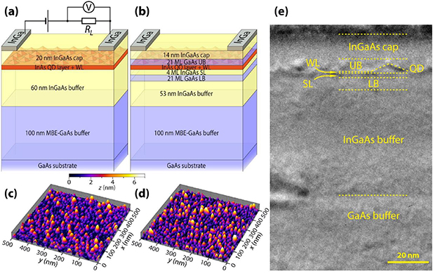
Figure 1. Schematics of the InAs/In0.15Ga0.85As QD structures without (a) and with GaAs CBs (b), together with representative AFM images of equivalent uncapped structures (c) and (d). The cross-section HRTEM image for the structure with CBs (e). The electrical contacts on the sample and connection for the photoelectric measurements are also shown in (a).
Download figure:
Standard image High-resolution imageThe morphology characterization of QDs in similar uncapped structures by atomic force microscopy (AFM) has shown that the QDs of both structures reveal similar sizes: 4 ± 1 nm height, 21 ± 4 nm diameter and surface density of 2.6 × 1011 cm–2 (figures 1(c) and (d)), where the data were collected from 1 × 1 µm images.
The cross-section high-resolution transmission electron microscopy (HRTEM) analysis confirmed the thicknesses of all the mentioned layers, as presented in figure 1(e) for the structure with both CBs. The images also show the pyramid-like QDs of different sizes averaging nearly 4 nm in height.
2.2. Photoelectric characterizations
PL spectra were acquired using a 532 nm laser as an excitation source with a power density of 5 W cm−2. For the in-plane dc photoelectric measurements, two bulk non-transparent InGa ohmic contacts were deposited onto both the samples, as shown in figures 1(a) and (b). In order to do this, InGa eutectic in a paste state was anointed onto the sample surface at room temperature. The current was measured as a voltage drop across a series load resistance of 1 MΩ, this value was much less than both the sample resistance and input resistance of the voltmeter. All the measurements were performed at a bias of 34 V. PC was excited by a 250 W halogen lamp light dispersed with a prism monochromator. The spectra were measured at 80 and 300 K and normalized to the lamp intensity. PC was measured twice per second, which allowed to register the long-term kinetics. All the optical excitation occurred under normal light incidence. To avoid an influence of possible defects caused by the contact deposition, the area near them was not illuminated.
2.3. TSC measurements
The deep level spectroscopy of TSC was performed at the same equipment and parameters as given in the previous Subsection, including the excitation energies and intensities, the technique is described in detail in our previous papers [18, 19]. First, a sample under the bias was cooled down in dark from 290 to 80 K, recording the dark current dependence on temperature. Then, the structures were excited by different energies, but the same quantum intensities, and various durations. The energies were QD PL spectrum peak positions and 1.4 eV, where InGaAs MB also absorbed. After the excitation, causing the trap filling by the generated carriers, the illumination was off, and the sample was kept for different times in dark till for the PC relaxation. After this delay, the heating with a constant rate of 10 K min−1 was on. As temperature increases, thermal escape of the captured carriers from the traps contributes to conductivity, herewith, the release temperature is determined by the trap depth. For the n-type semiconductor, the deep levels of electron and hole traps manifested as, respectively, the peaks and valleys on the background of temperature dependence of dark current. Since the dark conductivity shows exponential dependence on temperature, some TSC peaks related to deeper traps can be lost against the background. Therefore, we subtracted the dark current curve from TSC curves to obtain pure deep level TSC spectra.
2.4. Band calculations
Energy band profiles for QD structures (InGaAs layers, InAs wetting layer (WL), InAs QDs and GaAs CBs) were calculated using the Tibercad software [24], inclusive of strain effects and with realistic values of QD sizes, shape and composition [17, 25, 26]. A more detailed description of model calculations can be found in [27, 28].
3. Results and discussion
3.1. Photoluminescence characterization
PL spectra of the metamorphic InAs/In0.15Ga0.85As QD structures with and without GaAs CBs at different temperatures are shown in figures 2(a) and (b), respectively. PL of the structures is quenched with temperature due to the thermal escape of charge carriers from QDs to the continuum. The electrons and holes are known to escape as correlated pairs [29], however, the Mott formula fitting the temperature (T) quenching of PL intensity (IPL), shown in the insets of figure 2, contains two activation energies of non-radiative processes  1 and 2 [14, 21, 22]:


Figure 2. Temperature-dependent PL spectra of the InAs/In0.15Ga0.85As QDs in the structures without (a) and with GaAs CBs (b). Insets: the integrated PL intensities vs temperature (dots) and fitting by Mott formula (solid line).
Download figure:
Standard image High-resolution imagewhere k is the Boltzmann constant, I0 is the PL intensity at 0 K, and A, B are other fitting constants. The largest of activation energies corresponds to the direct escape of carriers from the ground quantum levels in QDs to the continuum, while the lowest one is usually attributed to defect-related nonradiative processes. The largest energies of the fitting are 0.19 and 0.32 eV for QDs without and with GaAs CBs, respectively, which are close to the values obtained in [14, 21, 22].
The pristine structure without CBs reveals the lower activation energy, and its PL is completely quenched at 300 K. In the following studies we assumed the QD PL spectrum position at 300 K to be similar to one in a recently studied InAs/In0.15Ga0.85As QD structure with thicker MB [16], i.e. peaked at 0.94 eV (∼1.32 µm) in the second telecommunication window. The growth of GaAs CBs improves the quantum confinement of charge carriers and limits their thermal escape from QDs, as indicated by the presence of a PL peak at room temperature from QDs near 1 eV (∼1.24 µm). The PL measured at 80 K (figure 3(b)) shows that the emission from the QD-CB structure, peaked at 1.08 eV (∼1.15 µm), is enhanced by about 200 times compared to the barrier-free PL at 1.02 eV (∼1.21 µm). Although the use of CBs hugely increases the PL yield, it blueshifts the spectrum by ∼ 60 meV due to increase of the confining potential for electrons (see band profile in figure 4). Nevertheless, the room temperature QD emission spectral range of the metamorphic structure with CBs, i.e. 1 eV (∼1.24 µm), still corresponds to the second telecom window. We have shown before that the QD emission can be technologically redshifted by varying the parameters of MB, such as higher In compositions [16, 30] or strain relaxation by increasing thickness [15, 31].

Figure 3. PC spectra of the InAs/In0.15Ga0.85As QD structures without (red) and with GaAs CBs (violet) at 300 (a) and 80 K (b). PL spectra of the structures without (orange) and with CBs (blue) are in arbitrary units.
Download figure:
Standard image High-resolution image
Figure 4. Band profiles across InAs QD in the structures without (a) or with GaAs CBs (b) at 300 (solid) and 80 K (dashed) calculated with Tibercad software [27, 28]. The point x = 0 corresponds to QD baseline.
Download figure:
Standard image High-resolution image3.2. Photocurrent spectroscopy and kinetics
The additional confining of QDs provides the enhancement of PL intensity, however, the alteration of QD properties may be substantial. We also focus our attention on an in-detail investigation of defect levels and their influence on the optical properties, characterizing the samples by means of dc PC and deep level TSC spectroscopies. PC spectra of the InAs/InGaAs QD structures at 300 and 80 K are given in figures 3(a) and (b), respectively. The spectrum shapes of both the samples are rather similar, as the onsets of the QD bands are not quite distinguishable. We can expect them to be close to those of the QD PL bands [18, 19, 30], i.e. QD response at 80 K should be above 0.95 eV and 1.03 eV, respectively, for the structures without and with CBs, while the barrier-confined QDs at 300 K are responsive above 0.96 eV. As for the pristine QDs, their PL is quenched, but the respective PL onset in similar structures with thicker MBs was found about 0.91 eV [19, 30]. These energies correspond to the QD interband transitions between the ground states in the largest QDs of main QD family.
The most prominent is that the QD response is suppressed for more than one order in the QD-CB structure. Definitely, in order to contribute to PC, charge carriers generated in QD should thermally escape out from the quantum confined levels into the respective bands of WL, which is the main conductivity channel in such lateral structures [18, 19, 30]. Electrons are the main charge carriers in such structures.
However, without CBs, the escape of electrons from QD levels into InGaAs layers or InAs WL levels seems to be much more probable [27]. It was shown [22] that the introduction of CBs into QD structure raises the level of WL for electrons, complicating their thermal escape from QDs to WL. Thus, the introduction of GaAs CBs should decrease their participation in conductivity, highly increasing the radiative recombination, and, conversely, cause a PC quenching. Naturally, the PC quenching appears more noticeable at 80 K, a temperature at which the thermal escape of electrons from QD to WL is much more reduced by CBs.
The PC component related to the In0.15Ga0.85As embedding layers also manifests in the spectra. The room temperature PC begins to decrease at 1.22 eV (figure 3(a)), where MB starts to absorb, presumably, through shallow levels below the conductivity band edge (Ec) [19, 30]. In0.15Ga0.85As bandgap (Eg) calculated within Varshni theory is 1.256 eV for 60 nm thick MB [27], and we can see an additional step at this energy in both the samples. The band-to-level and band-to-band transitions in In0.15Ga0.85As layers lead to the generation of free electrons and holes. Possibly, the generation of free holes results in a decrease of the total signal. According to the band profile calculation (figure 4), electrons generated in In0.15Ga0.85As are possibly affected by an increased potential field of the heterojunction around the QD layer. Meanwhile, the field formed near the QD layer can force holes towards the InAs nanostructure. As a result, holes can be directly captured by QDs or WL and recombine with free electrons generated there. This may cause a decrease of conductivity, resulting in the PC drop. Such a mechanism might be the same in both the samples, since GaAs CBs does not introduce significant energy barriers in the valence band. However, in contrast to the room-temperature spectra, no decrease in the 80 K PC signal is observed at the excitation above In0.15Ga0.85As Eg (1.31 eV). We assume that free holes generated in In0.15Ga0.85As cannot affect the WL conductivity channel at low temperatures due to an inferior mobility and high possibility to be captured by hole traps (determined by TSC below). On the contrary, we observe an increase in PC above 1.3 eV in the QD-CB structure in figure 3(b). Obviously, the In0.15Ga0.85As PC is just less suppressed by the CB occurrence than the QD band, for the reason that some charge carriers are able to directly come to the contacts.
The shapes of PC spectra for both the structures faintly change by varying excitation density (figure S1, supplementary materials) (available online at stacks.iop.org/SST/35/095022/mmedia). The PC dependences on excitation intensity (I), measured at energies of all the main PC and PL components, are typical for low-doped semiconductor and they are shown in figure 5. At low intensities, while equilibrium charge carriers dominate the non-equilibrium ones, the dependence is linear. At higher intensities, as nonequilibrium electrons become dominant, it transforms to PC(I) ∼ I0.5. This is more notable for the edge excitation of bulk GaAs (reference Eg of 1.435 and 1.51 eV at 300 and 80 K, respectively) and InGaAs MB (1.256 and 1.31 eV at 300 and 80 K, respectively), an absorption spectrum of a similar structure can be seen in [17]. In QDs (excitation at energies ≤ 1.2 eV), such transformation expectably occurs at higher energies due to much higher concentration of equilibrium electrons: this is illustrated by a specific band bending in figures 4(a) and (b). As the thermal escape of photogenerated carriers from the QDs in CBs is suppressed, the transformation of linear dependence to PC(I) ∼ I0.5 at the QD excitation (black and red dependences) is notable to start at lower intensities than in the pristine structure and occurs slower when the excitation increases. So, 2-fold deviation of the experimental values from the linear fitting is found above 2 mW cm−2 without CBs vs 0.1 mW cm−2 with CBs.

Figure 5. PC vs excitation intensity for the InAs/In0.15Ga0.85As QD structures without (a) and with GaAs CBs (b) at 300 K in different points of the spectra: the QD transitions at PL peak (black), the transitions in all the QD ensemble (red), as well as the effective band-to-band excitation of InGaAs MB (green) and GaAs (blue). The dashed lines are the fitting by functions PC(I) ∼ Iα.
Download figure:
Standard image High-resolution imageThe edge of PC signal at ∼ 0.7 eV is attributed to the response from the defects, firstly, to EL2 states present in the GaAs buffer and substrate of metamorphic structures and usually detected above 0.75 eV [18, 19, 30, 32]. The weak PL band peaked at 0.79 eV in figure 3(b) may be also related to the radiative transitions from Ec to EL2 levels.
EL2 defects also manifest themselves in the temperature dependencies of dark current (figure 6). Each of them shows two sections well fitted by functions  , where is the conductivity activation energy. In particular, the dependencies at higher temperatures reveal the values ∼ 0.75 eV, which is very close to the one characteristic for EL2 level known as a recombination center [33]. When heating from lower temperatures, the conductivity is activated by different ways in both the samples. The structure with CBs reveals a curve with ≈ 0.57 eV, which is close to the activation energy of GaAs-inherent point defect (PD) EL3 found also in QD structures based on GaAs, or extended defect ED1 found in metamorphic structures [18, 19]. As for the pristine structure, a notably higher energy of 0.69 eV is obtained. So, we can relate ED1 defect with the activation energy about 0.57 eV to threading dislocations known to propagate over In0.15Ga0.85As MB, originating from InGaAs/GaAs interface [16].

Figure 6. Temperature dependences of dark current for the InAs/In0.15Ga0.85As QD structures without (red) and with GaAs CBs (blue) and approximations of their parts by the functions  (black and green lines).
Download figure:
Standard image High-resolution imageThe structural defects affect the mechanism of carrier transport at low temperatures, that can be investigated by analyzing the time dependences of PC (figure 7). The PC kinetics after the start of illumination is complex: a monotonous decrement of PC under the constant illumination after the initial fast increase. Such a kinetics was recently reported by us for similar InAs/InxGa1–xAs QD structures without CBs, including x = 0.15 [19]. The effect was explained by a Coulomb screening of WL, as an in-plane conductivity channel, by the charged electron traps located near QDs. The induced electric potential inhibits the charge carriers incoming from outside, the detailed reasoning and assumptions are given in our previous study [19].
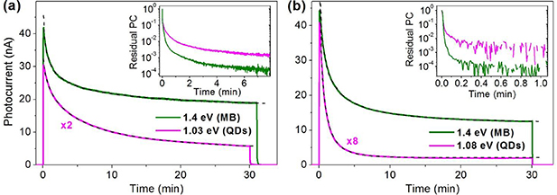
Figure 7. PC dependence on time of the InAs/In0.15Ga0.85As QD structures without (a) and with GaAs CBs (b) at 80 K under the continuous excitation at the energies of QD PL peak and MB resonant pumping, the dashed lines are fitting with allometric exponents. The point (0, 0) corresponds to the start of excitation. Insets: PC decay after the excitation off (point t = 0), where the curves are normalized to the values at t = 0.
Download figure:
Standard image High-resolution imageThe conductivity decrement under the constant illumination is well fitted by allometric exponents

where σ0 is the stationary conductivity at t → ∞, A is a decrement amplitude, τ is a time constant, and β < 1 is a dispersion factor. The allometric functions are usually observed in structurally disordered systems and originated from continuous sets of simple functions (exponents or hyperbolas) with different decay parameters [34].
The fitting time constants and dispersion factors are summarized in table 1. The barrier-free structure shows the fitting parameters τ = 3.82 min and β = 0.53 for the resonant QD excitation (1.03 eV), and τ = 2 s and β = 0.18 under 1.4 eV, involving photogeneration in QD, WL and the edge absorption in In0.15Ga0.85As MB (figure 7(a)). The values of time constants are slightly different from those observed for the InAs/In0.15Ga0.85As QD structure with a 500 nm thick MB studied in the previous paper [19]; however, τ for the low-energy excitation is much longer than that for 1.4 eV. Here, unlike the previous study, the dispersion factor β under 1.03 eV in our structure on a thinner MB is essentially higher, which causes the PC decrement to be no more prolonged than under 1.4 eV. Otherwise, the QD-CB structure reveals τ = 23 s and 25 s for 1.08 eV and 1.4 eV excitation, respectively, whereas corresponding values β = 0.54 and 0.36 (figure 7(b)). Thus, CBs lead to comparable time constants of the decrement for both the excitation energies and increase in the dispersion factor under 1.4 eV excitation, while β for resonant QD excitation remains unchanged.
Table 1. Fitting parameters for PC degradation in the studied QD structures under different excitation energies.
| Barrier-free structure | Structure with GaAs CBs | |||
|---|---|---|---|---|
| Fitting parameter | 1.03 eV (QD exc.) | 1.4 eV | 1.08 eV (QD exc.) | 1.4 eV |
| τ (s) | 229 | 2 | 23 | 25 |
| β | 0.53 | 0.18 | 0.54 | 0.36 |
Furthermore, the presence of CBs accelerates the PC relaxation after switching the illumination off (insets in figure 7). It is worth to note that the decay kinetics after the MB band-to-band excitation (1.4 eV) is faster than that after the resonant QD excitation in both the samples, unlike in the previous study [19], when the PC decay after the MB excitation was slower. This is reasonable since much thicker MB contributed to the PC in the previous study. The kinetics features could be also caused by diverse density of traps present in the structures.
3.3. Deep level TSC study
To study the deep levels in-detail, TSC measurements were carried out (figure 8). We have found a sequence of bands caused by the traps on the current dependence on increased temperature for the post-illuminated structures. As the bands are overlapped, the activation energies of traps were roughly estimated as ≈ 23 × kTm, where Tm is the temperature at the band peak.

Figure 8. Deep level TSC spectra of the InAs/In0.15Ga0.85As QD structures without (a), (b) and with GaAs CBs (c), (d) excited at QD PL peak (a), (c) and 1.4 eV (b), (d) for different times of light pumping/delay. The intensities above 265 K (a), (b) and 255 K (c), (d) are rescaled. The activation energies in eV of found traps are labeled in (a) for convenient analysis and comparison with data from table 2.
Download figure:
Standard image High-resolution image
Table 2. Trap levels detected in the studied metamorphic InAs/In0.15Ga0.85As QD structures.
| Activation energy (eV) | Designation | Origin |
|---|---|---|
| 0.17 | EL10 | PDs at InAs/InGaAs interface [18–20, 35–37] |
| 0.22 | EL9 | PDs at InAs/InGaAs interface [18, 19, 36, 37] |
| 0.27 | EL8 | PDs at InAs/InGaAs interface [19, 35] |
| 0.28 | EL7 | PDs at InAs/InGaAs interface [18–20] |
| 0.30 | ED4 | EDs or related PDs at dislocation line [18, 19] |
| 0.37 | EL6 | PDs at InAs/InGaAs interface [18, 19, 36, 37] |
| 0.43 | ED3, EL5 | EDs or related PDs in InGaAs MB [16, 18–20] |
| 0.47 | ED2, EL4 | EDs or related PDs at InAs/InGaAs interface and in MB [18, 19] |
| 0.53 | ED1, EL3 | EDs or related PDs at InAs/InGaAs interface and in MB [18–20] |
| 0.55 | HL3 | EDs originated at InGaAs/GaAs interface [35] |
Identification of most of the existing traps by their activation energies has been described earlier [18, 19]. Thus, GaAs-inherent PDs EL10 (Ec—0.17 eV), EL9 (0.22 eV) and EL7 (0.28 eV) are the shallowest levels found in all the spectra at ∼ 87, 111 and 140 K, respectively. A deeper PD, EL6 (0.37 eV), is observed near 183 K in both the structures only after the prolonged (30 min) resonant excitation of QDs, the shorter illumination (30 s) or that at 1.4 eV reveals no evidence of this defect. Otherwise, a weak band of EL8 PD near 135 K (0.27 eV) is observed in the sample without CBs only after the short-term (30 s) QD excitation (figure 8(a), blue curve). Amplitudes of all the mentioned traps are notably higher at the resonant QD excitation, hence, they are obviously located predominantly near the QD layer.
Beside PDs, signatures of EDs are found. An intense band peaked at 218 K is attributed to ED named as ED3 (0.43 eV) [18, 19], it is followed by the weaker band of ED2 (243 K, 0.47 eV). In turn, it should be followed by the next intense band of ED1 defect (0.52–0.54 eV) usually peaked near 265 K [18, 19], however, its shape is distorted by an intense feature at higher temperatures, discussed below. Furthermore, there is a band manifesting in all the spectra as a weak feature at the slope of EL7-related band. Its position near 153–155 K corresponds to the activation energy of 0.30–0.31 eV. Recently [19], such a feature was found in TSC spectra of metamorphic structures and assumed to be originated from Frenkel pairs VAs–Asi (EL7 PDs) accumulated at dislocation lines. Thus, we mark this defect as ED4.
Heating from 260 to 290 K, the current passes below the dark current temperature dependence, that means the release of positive charge carriers from a hole trap. The response of this trap results in a deep valley on the TSC curve and has the highest amplitude. Overlapping the ED1 band, it inhibits completely or weakens this band to a great extent; it is worth noticing that the ED1 band was the most intense in the InAs/In0.15Ga0.85As QD structures studied earlier [18, 19]. Its activation energy can be roughly estimated considering the band minimum in the QD-CB sample, where it is most intense and the effect of neighbor bands is negligible. The minimum near 276 K corresponds to the activation energy of ∼ 0.55 eV. This value is close to that of the known HL3 hole trap inherent in GaAs [38]. This trap was also observed in In(Ga)As/GaAs QD structures [35], but not detected to date in metamorphic QD ones. We should notice that the previously studied metamorphic QDs [18–20] were grown on thick MBs (500 nm), diminishing the effect of threading dislocations propagating form InGaAs/GaAs interface toward the surface. Hence, we may attribute the deep hole trap HL3 to the threading dislocations manifesting in TSC due to the closer InGaAs/GaAs interface. The relative signal from hole trap HL3 after 1.4 eV excitation is increased by more than 2 times in the QD-CB structure. Hence, this trap can be attributed to the InGaAs/GaAs interface of CBs. The found traps and their interpretation are given in table 2 together with data on possible relation to PDs or EDs and location of the trap levels in the nanostructures.
Comparing the composition of TSC spectra for both the structures, we can conclude that the introduction of GaAs CBs into InAs/InGaAs QD structure does not lead to the generation of new types of traps. Analyzing the amplitude of TSC peaks, it should be noted that the structure with GaAs CBs reveals less electron trap responses. While the strong effect for the MB excitation (1.4 eV) might be explained by a diminution of the released carriers to WL through the wide-gap barriers, but we also observe a notable reduction of TSC signal after the resonant QD excitation, when there are no obstacles for generated charge carriers to leak into WL. However, a conclusion about lower amount of defects in the structure with CBs could be premature, if one compares PC signals for both the samples. At 80 K, the pristine structure reveals a photoresponse 4-fold at 1.4 eV and one-two order higher at the PL peak, where the resonant QD pre-excitation was realized. PC is determined by the amount of non-equilibrium carriers, which, in turn, also affects directly the trap filling. Thus, the lower TSC signal in the QD-CB structure can be due to a lower population of the levels by the trapped carriers. Furthermore, the collection of released carriers into the WL conductivity channel should be considered. GaAs CBs prevent the motion of carriers generated in MB toward WL, thus increasing the probability of their back-capturing and recombination. This causes a lower TSC response in the QD-CB structure.
So, we can draw no definite conclusion about the change in the defect amount in the QD structures as a result of the GaAs CB introduction, if we consider only TSC results. However, there is an indirect evidence of an increase in the defect density. Analyzing the time dependences of PC in figure 7, one can see that the decrement of PC under the continuous resonant QD excitations is faster and more drastic in the QD-CB structure. This can indicate an increase in the electron trapping due to defect traps in vicinity of QDs grown with additional barriers. It is known that a large amount of PDs and EDs is concentrated near QD layers in InAs/InGaAs structures [18–20], and also in InAs/GaAs ones [16, 39]. Interfaces between materials with lattice mismatch can cause the generation of such defects related to strain relaxation.
Again, in metamorphic structures the mismatch between InAs QDs and InGaAs embedding layers is reduced in comparison with conventional InAs/GaAs QD structures. Thereby, the deposition of even thin GaAs layer on InAs/InGaAs QDs before the InGaAs cap can result in an increase of the strain and it might result in additional defects as the hole trap HL3, although the electron trap spectrum is the same. Also, the assumption about additional traps in the QD-CB structure can be confirmed by the temperature dependence of dark current, where a contribution of ED1 state at 0.57 eV to the conductivity is detected, unlike the case of the pristine structure without CBs.
These data lead us to conclude that the growth of GaAs CBs allows to enhance by more than two orders of magnitude the PL emission intensity from metamorphic InAs/InGaAs QDs in the second telecommunication window at 1.3 µm at room temperature and 80 K, at the cost of a blueshift of the emission peak. We have found that the presence of GaAs CBs also alters carrier transport. It increases the thermal activation energy of electrons confined in QD, causing PC quenching. At low temperatures, CBs may also block the capturing of electrons generated in InGaAs by QD and WL and, on the other hand, prevent the trapping of electrons outside the QD layer, decreasing carrier lifetimes. The deep levels, identified as PDs and EDs inherent in GaAs (or InGaAs), have been detected to be similar in both the structures. The difference is only in the relative contribution of various traps to the TSC spectra, with the total response being lower in the QD-CB structure. We conclude that there are no new types of defects introduced in the structure by adding CBs into the QD structure, but this change in design causes a slightly increased density of traps near QDs.
As a matter of fact, we have analyzed in depth the carrier transport mechanisms and we have clarified the origin of defects that influence the PC in both the structures. From these data and their interpretation based on other reports, some indications for the use of wide-bandgap CBs in InAs/InGaAs QDs for IR lasers may be highlighted:
(i) GaAs CBs allow for consistent enhancement of the PL emission intensity; however, extreme care must be payed to the growth of buffer and active layers to reduce the defect density, as they act as recombination and trap centers highly increasing non-radiative recombination and response time [18, 19];
(ii) thick MB of ≥ 500 nm should be employed to overcome strain-related defects like threading dislocations induced by the lattice mismatch near InGaAs MB/GaAs substrate interface [15–19, 40];
(iii) to shift the photoresponsivity towards third telecom window (1.55 µm) or achieve broad-band light sources, advanced multi-layer designs allowing strain-relaxation should be used, in particular, In-rich InGaAs MBs; this was done for the development of metamorphic InAs/InGaAs QDs [13, 30, 41, 42] and IR QD cameras [3, 4, 43];
(iv) the addition of GaAs CBs to low-density metamorphic InAs QDs should allow for an increase in the emission efficiency of single QD PL, that can foster the development of single-photon emitters operating in the IR range 1.3–1.55 µm [10, 11, 28];
(v) multi-layer stacks of QDs equipped with CBs (50–100 layers) are needed to obtain an efficient IR emission allowing application in ultra-large bit rate and energy-efficient QD lasers and optical amplifiers [1, 8, 9].
4. Conclusions
The metamorphic InAs/In0.15Ga0.85As QD structure with and without GaAs CBs grown on GaAs have been studied by PL, PC and TSC. The growth of CBs allows for room temperature PL emission at 1.3 µm and to enhance the low-temperature emission by more than two orders of magnitude, though the emission peak blueshifts. We also focus on an in-detail investigation of carrier transport and defect-related deep levels. GaAs CBs decrease the thermal activation rate of electrons confined in QD and WL, thereby highly increasing the radiative recombination, causing PC quenching. At low temperatures, CBs may also block the capturing of electrons generated in InGaAs by QD and WL and, on the other hand, prevent the trapping of electrons outside the QD layer, decreasing carrier lifetimes. The deep levels identified as PDs and EDs inherent in GaAs (or InGaAs) have been detected in both the structures. A new hole trap identified as HL3, undiscovered earlier in these nanostructures, has been detected in the structure with CBs. There are no new types of defects appeared in the structure by growing CBs into the QD structure, but this causes a slightly increased density of traps near the QDs in GaAs CBs as compared to the pristine structure without barriers.
We hope that these results and outcomes could be useful for the design of strain-relaxed InAs/InGaAs QDs aiming at IR light emitters and foster further development of energy-efficient QD lasers, optical amplifiers and single-photon emitters operating in the IR range 1.3–1.55 µm.
Acknowledgments
This work was supported in part by National Natural Science Foundation of China [61604098, 61525503, 61620106016]; Shenzhen Science and Technology Innovation Commission under Grant of China [JCYJ20170412110137562]; Shenzhen University Scientific Research Start-up Foundation of China [860-000002110207]; Ministry of Education and Science of Ukraine [0119U100308].
Notes
The authors declare no competing financial interest.