

Abstract
Graphene-on-semiconductor heterojunction solar cell is an emerging class of photovoltaics (PV) with potential for efficient and reliable energy conversion systems. The interface between graphene and a lightly doped semiconductor plays a key role in charge-carrier separation and recombination dynamics. Owing to the low Schottky barrier height (ϕSBH)-induced interfacial charge carrier recombination, graphene-on-silicon (Si) heterojunction solar cells suffer from instability in power conversion efficiency over time. Therefore, it is critical to engineer the interface to enhance the barrier height by interfacing a chemically stable, insulating, and atomically thin layer. Further, the temperature dependent photovoltaic characteristics of such stacked architectures are unknown, and temperature dependent behavior is critical to understand the metal-insulator-semiconductor (MIS) junction behavior and photovoltaic phenomenon. Here, we have introduced hexagonal boron nitride (h-BN) as a tunneling interlayer in graphene-on-Si heterojunction solar cells, which enables the passivation of the chemical dangling bonds on the Si surface. The effect of temperature on the performance of a graphene/h-BN/Si PV cell is examined. Thin films of h-BN are directly synthesized on a lightly doped Si surface via a bottom-up chemical-surface-adsorption strategy followed by the transfer of a graphene monolayer. The 2D layer-on-2D layer-on-3D bulk semiconductor nanoarchitecture of graphene/h-BN/Si forms a MIS-type junction, where the h-BN acts as an electron-blocking layer to avoid interfacial charge carrier recombination. A four-fold increase in open-circuit voltage (Voc) is found for the graphene/h-BN/Si heterojunction cell (0.52 V) in contrast to the graphene/Si cell (0.13 V), which is due to the increase in the ϕSBH and hence built-in electric potential. Interestingly, the Voc linearly decreases by only ~4% with every 10 K increase in temperature. This work will lead to the evolution of new 2D/2D/3D nanoarchitectures for mechanically robust, high performance, and durable optoelectronic functionalities.
Export citation and abstract BibTeX RIS
1. Introduction
Owing to its high optical transparency and ultra-high charge carrier mobility, sp2-hybridized graphene [1–3], which can function both as a transparent electrode and an active layer, is a potential candidate two-dimensional (2D) material for photonics, optoelectronics, and photovoltaics. A rectifying Schottky junction can be constructed by interfacing graphene with lightly doped silicon (Si), which can be employed as a photovoltaic cell [4] under the irradiation of light. The graphene-on-semiconductor heterostructure, which has the benefit of a cost-effective fabrication process, has shown a promising power conversion efficiency of over 10% at AM 1.5 G irradiation with functionalized or doped graphene [5–11] and with an anti-reflection layer [12–15]. However, the graphene/Si-based 2D layer-on-3D bulk semiconductor solar cell suffers from serious instability in photovoltaic performance [16]. This stems from the existence of an astronomically high dark current in the graphene/Si Schottky barrier junctions, which is caused by the thermionic-emission-based dark current [17]. What is more, mid-gap surface states can be formed by dangling bonds on the Si surface, which will provide an additional pathway for the charge carrier recombination [18].
To reduce the thermionic-emission-based dark current and charge-carrier recombination, a non-reactive and stable passivation layer is required to separate the metal and semiconductor by forming a metal-insulator-semiconductor (MIS) architecture [19]. Previously, thin film insulators like transferred hexagonal boron nitride (h-BN) [20], silicon dioxide (SiO2) [21], Al2O3 [22], and fluorographene (FG) [23] have been reported as an electron blocking layer in MIS structure for photovoltaic application. Unlike SiO2 and FG [21], the h-BN layer does not have trapcharges and surface states [24, 25]. h-BN is a sp2-hybridized 2D insulator with wide energy bandgap of 5.97 eV and ultra-smooth surface with no surface-dangling bonds [26–28]. Further, h-BN is isostructural and isoelectronic to graphene with a lattice mismatching of only 1.7%, thus enabling a compatible graphene/h-BN heterostructure [29]. A similar MIS structure has been built by transferring the h-BN layer [20] onto the Si surface, which can introduce heteroatom contamination during the chemical-transfer process [30]. Therefore, direct growth of h-BN on the Si surface is critical to avoid defects and for scalability. The temperature dependent diode and photovoltaic characteristics of the graphene/h-BN/n-Si heterojunction solar cell can be crucial to understand the charger carrier separation and recombination dynamics at the MIS structure interface. Previously, Kalita et al conducted a temperature dependent study on a metal-semiconductor (MS)-type graphene-GaN heterojunction and an MIS-type graphene/h-BN/GaN in the range of 298–373 K [31, 32]. The graphene-GaN heterojunction showed a photovoltaic effect and its open-circuit voltage (Voc) decreased nonlinearly with the temperature. The graphene/h-BN/GaN heterojunction showed an increased Schottky barrier height (ϕSBH). Temperature dependent studies of Si-based MIS solar cells have been explored in many previous studies [33]. However, no temperature dependent photovoltaic characteristic of graphene based MIS structure has been reported. It is therefore critical to investigate the temperature dependent photovoltaic characteristics of a graphene/h-BN/n-Si heterojunction device.
In this work, we directly nucleated an h-BN layer on an n-type silicon (n-Si) surface via a surface-chemical-interaction mechanism [25, 34]. A chemical-vapor deposited single-layer graphene was transferred to the top of the h-BN to construct a graphene/h-BN/n-Si MIS-type heterostructure. Temperature dependent photovoltaic characteristics are investigated. The Voc of a maximum of 0.52 V is achieved merely by introducing an h-BN interlayer, which is a four-fold increase in comparison to the graphene/n-Si heterojunction cell. An energy-band model is developed to determine the effective Schottky barrier height (ϕ'SBH) of the graphene/h-BN/n-Si heterostructure after incorporating the h-BN layer.
2. Experimental
The fabrication process of a graphene/h-BN/Si solar cell is schematically illustrated in figure 1 (a). h-BN thin films were directly synthesized on a 1 × 1 cm2 solar grade lightly doped n-Si by low-pressure chemical vapor deposition (LPCVD) as reported in the literature [25]. The process steps are presented in the Materials and methods section. Monolayer graphene was synthesized on copper foil (99.8%, Alfa-Aesar) using thermal LPCVD and transferred onto an h-BN/n-Si chip using the standard poly(methyl methacrylate) (PMMA) transfer method as reported previously [35]. The copper was removed by immersing the PMMA coated graphene/copper into an acid solution consisting of 1 part HNO3 and 1 part deionized (DI) water under ambient temperature for 10 min. The PMMA was removed by immersing the graphene-coated sample in the 60 °C heated-acetone bath for 10 min. Both the process of the synthesis of graphene on metal catalyst substrates and its chemical transfer are presented in the Materials and methods section. For the fabrication of the heterojunction device, a titanium (10 nm)/gold (50 nm) pattern was made by standard e-beam evaporation and the lift-off lithography strategy. A gallium-indium eutectic (99.99% Aldrich) was used as the back-contact metal electrode for the graphene/h-BN/n-Si cell. Raman spectra were acquired by a confocal Raman microscope (Raman-AFM, WITec alpha 300 RA, laser wavelength of 532 nm and beam size of 721 nm). Light and dark current density/voltage (J-V) characteristic profiles were acquired under AM1.5G illumination (100 mWcm−2) and a dark condition using a Keithley 2612 source measurement unit. The quantum efficiency measurement (wavelength range: 200–1100 nm) facility was created in-house with a monochromator provided by ORIEL Instruments. Temperature dependent studies were conducted with a Janis ST-100 setup.

Figure 1. (a) Schematic of the graphene/h-BN/n-Si solar cell development process steps. (b) Optical image of the cell with an effective area of 0.25 cm2.
Download figure:
Standard image High-resolution image3. Results and discussion
Raman vibrational spectroscopy is typically employed to identify chemical and electronic structures by observing vibrational, rotational, and other low-frequency modes in a material system [18]. Raman spectroscopy has been extensively utilized as an inelastic-scattering based fingerprint to characterize 2D nanomaterials [36–38]. Scanning Raman spectra and mapping results are presented in figure 2 to confirm the nucleation of h-BN on n-Si and the formation of a graphene/h-BN heterostructure. The presence of a weak peak at 1368.8 cm−1 in the h-BN/n-Si Raman spectrum (figure 2(a)) corresponds to the E2g in-plane vibration of boron and nitrogen atoms in the molecular building unit of h-BN as shown in the inset [39]. There are also no competing Raman peaks such as 1304 cm−1 and 1055 cm−1 which correspond to the longitudinal optical phonon and the transversal optical phonon of c-BN [38]. The color circles (black, green, blue, red, and purple) at different areas of figure 2(b) correspond to the Raman spectrum of the same color in figure 2(a). The homogeneous color contrast in figure 2(b) and the presence of 1368 cm−1 Raman peaks in all the Raman spectra in figure 2(a) clearly show a continuous and uniform h-BN film formation on solar grade light p-doped n-Si surfaces [34]. Further, for the graphene/h-BN/n-Si hybrid system, two characteristic Raman modes at 1583 cm−1 (G-peak) and 2687 cm−1 (2D peak) are found, which demonstrate the continuous interfacing of graphene on the h-BN surface. It is noted that the Raman shift of this graphene's G-peak is less than 1584.5 cm−1, which indicates a lightly doped graphene [40]. To further confirm the uniformity of the graphene/h-BN heterostructure, spatial Raman mapping for graphene's D peak (1344 cm−1), G peak (1583 cm−1), and 2D peak (2687 cm−1) are presented in figures 2(d), (e) and (f). The colored circles (blue, red, and black) at different areas of figures 2(d)–(f) correspond to the Raman spectra of the same color in figure 2(c). The homogeneous color contrast in figures 2(d)–(f) clearly shows a continuous and uniformly transferred graphene on the h-BN/n-Si surface.

Figure 2. Raman characterization of h-BN and the graphene/h-BN heterostructure: (a) Raman spectrum shows the E2g vibrational mode of h-BN produced directly on the n-Si surface with the in-plane atomic vibration in the inset, while the assorted color lines represent the assorted color dots in (b). (b) Spatial Raman mapping of h-BN's E2g peak. (c) Raman spectra for graphene on h-BN/Si, while the assorted color lines represent the assorted color dots in (d)–(f). Spatial Raman mapping of graphene's D peak (d), G peak (e), and 2D peak (f).
Download figure:
Standard image High-resolution imagePhoto-electrical measurements are essential to investigate the performance of photovoltaic cells. Figure 3(a) shows the photovoltaic profile of the graphene/h-BN/n-Si solar cell. As expected, the performance of the device with h-BN as an interlayer increased in comparison to the reference graphene/n-Si solar cell. The photovoltaic characteristics, such as the Voc, short-circuit current density (Jsc), and fill factor of the graphene/h-BN/n-Si device are 0.52 V, 0.57 mA cm−2, and 25%. The measured Voc for the graphene/n-Si solar cell is about 0.13 V as shown in the inset of figure 3(a). It is interesting to observe that the Voc is enhanced four-fold by inserting a thin film of h-BN layer between the graphene and n-Si. Further, it is critical to understand the recombination dynamics in the graphene/h-BN/n-Si photovoltaic cell. The external quantum efficiency (EQE) is a spectro-electronic tool and it is the ratio of the number of charge carriers collected by the solar cell to the number of incident photons of a given wavelength. As presented in figure 3(b), it is found that the cell exhibits a higher EQE (30%–50%) in the longer wavelength range of 600–800 nm. A lower EQE indicates a higher recombination in the short wavelength range: 300–600 nm. As illustrated in figure 3(c), the photo-excited charge carriers are separated by the built-in electric potential (Vbi), where the holes are pulled to the graphene electrode and the electrons toward n-Si. Here, the sum of Vbi and ΔE (ΔE = Ec–Ef) is known as the ϕSBH, which blocks the transport of electrons from the n-Si back to the graphene and the holes from the graphene back to the n-Si. However, the ϕSBH is relatively low for a graphene/Si heterojunction, so electrons may drift back to the graphene, and that may cause a current leakage. To reduce the current leakage, an h-BN layer is introduced between the graphene and the n-Si to increase the ϕSBH and thus create an extra barrier for electrons drifting back to the graphene/h-BN/n-Si interface. The ϕ'SBH in figure 3(d) is larger than the ϕSBH due to the insertion of an h-BN layer.

Figure 3. Photovoltaic measurement on the graphene/h-BN/n-silicon solar cell: (a) illuminated J-V characteristics of the graphene/h-BN/n-Si solar cell. The inset shows illuminated J-V characteristics of the graphene/Si cell. (b) Quantum efficiency of the graphene/h-BN/Si solar cell. Energy band structure diagram of the graphene/n-Si heterojunction without h-BN (c) and with h-BN (d) as an interlayer.
Download figure:
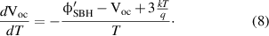
Standard image High-resolution imageThe J-V profile under a dark condition is critical for understanding the electrical performance of a diode. Figure 4(a) shows the dark J-V characteristics of the graphene/h-BN/n-Si MIS-type heterojunction cell with a variation in temperature (300–375 K). An increased forward current under forward bias, as well as an increased reverse current, were observed with the increased temperature for the applied voltage ranging from −0.2 to 0.6 V. Similar phenomenon has been reported for a Si-based MIS structure solar cell and a graphene-based MS structure heterojunction solar cell [41, 42]. As shown in equation (6), the Voc decreases as the dark saturation current (Js) increases. The intrinsic carrier concentration increases as the bandgap of the Si decreases with the increase in the temperature. The result is in accordance with realistic dark J-V characteristics [43]. Figure 4(b) shows the log(|J|)-V plot in the voltage range of −0.2 V to 0.6 V with the increase of temperature. The series resistance was derived from the dark J-V curve as shown in figure 4(c) [44]. Detailed Rs values under different temperatures are displayed in figure 4(c), and show that the series resistance of the graphene/h-BN/n-Si solar cell decreases as the temperature increases. For every 25 K increase in temperature, the series resistance decreases by approximately 45%. The ϕSBH can be calculated through combining equations (1) and (6). The ϕSBH versus temperature is plotted in figure 4(d), and the effect of heat on the ϕ'SBH is depicted in figure 3(d). The ϕSBH decreases with temperature and with the decrease of the ϕSBH, electrons can more easily diffuse back to the interface and recombine with the holes and thus the efficiency of the solar cell decreases due to a higher recombination.

Figure 4. Temperature dependency of the graphene/h-BN/n-Si solar cell without light illumination: (a) J-V characteristics, (b) log(|J|)–V plot under different temperatures. (c) Series resistance derived from dark J-V characteristics. (d) The effect of temperature on the ϕSBH and series resistance.
Download figure:
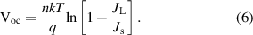
Standard image High-resolution imageThe photovoltaic characteristics of the graphene/h-BN/n-Si solar cell as a function of temperature are critical to understand the role of thermal energy in exciton carrier transport. A photovoltaic effect was obtained and is illustrated in figure 5(a) for all the temperatures studied. As shown by the gray arrow in figure 5(a), the Voc decreases as the temperature increases. The changes of Voc with temperature are plotted in figure 5(b) and a detailed calculation is presented in section 2 of the supporting information (stacks.iop.org/SST/35/075020/mmedia). A linear fit was performed on the data points of Voc versus temperature. The R2 is 0.999, which means the Voc is linear to temperature and the Voc decreases by 2.0 mV for every 1 K increase in temperature. This linear property of Voc versus temperature is exactly the same as that of the Si solar cell (2.0 mV) [41]. At the same time, Jsc remains almost the same (variance is 4.1x10⁻⁵) when the temperature increases from 300–375 K (figure 5(b)).

Figure 5. Temperature dependency of the graphene/h-BN/n-Si solar cell under AM 1.5 G light illumination: (a) illuminated J-V characteristics under different temperatures. (b) Voc and Jsc changes with temperature.
Download figure:
Standard image High-resolution image
In order to further analyze the effect of temperature on the MIS structure of the graphene/h-BN/n-Si solar cell and the effect of the h-BN layer, we analyzed their J-V relations as presented below [45]:
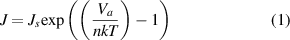
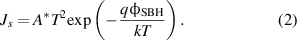
Here J and Jsare the current density and reverse saturation current density, respectively [17], A* is the effective Richardson constant, T is temperature, k is the Boltzmann constant, and ΦSBH is the Schottky barrier height.
The small red shift of the graphene G-peak indicates a lightly doped graphene, and the photovoltaic effect of the graphene/h-BN/n-silicon heterostructure further indicates a slightly p-doped graphene. Although graphene under an ambient environment is slightly p-doped, it still behaves as a metallic electrode [46]. Adding an h-BN tunneling layer will add a tunneling probability factor of  [47]. Now, the
  can be expressed as:
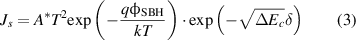
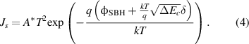
The new  by comparing equations (1) and (3) is:

According to equation (5), the  is increased by
  due to the insertion of the h-BN layer. The conduction band offset (ΔEc) represents the effective tunneling barrier height that the h-BN layer creates for the electrons in the conduction band of the n-Si. For the graphene/h-BN/n-Si heterostructure, the ΔEc is the work function of the n-Si, which is approximately 4.1 eV and
  is the thickness of the h-BN film. As is shown by equation (5), the ΔEc and thickness affect the Js exponentially.
The Voc of the solar cell can be expressed as [48]:
Here JL is the light generated current density, Js is the dark saturation current density, which is composed of Jms (thermionic emission dark current), Jrg (depletion layer recombination-generation current density), Jd (injection diffusion current density), and Jss (surface state current density due to the charge exchange between the metal and semiconductor band edges via surface states). We mainly focus on the effect of Jms on the Js since the large Jms is the main cause for the high dark current for the MS heterojunctions. According to equation (4), the Jms decreases with the increase of the  . Since JL remains the same for the same graphene/n-Si heterojunction, the Voc increases as the Js decreases with the insertion of the h-BN layer in the graphene/n-Si solar cell.
The relation of the saturation current density and diffusion length can be expressed as follows [49, 50]:
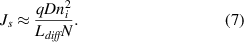
Here D is the diffusivity of the minority carrier, Ldiff is the minority carrier diffusion length, N is the doping, and ni is the intrinsic carrier concentration. According to equation (7), the dark saturation current density is positive dependent on ni, and ni increases with temperature. By combining equation (7) and the equation for the intrinsic carrier concentration, we get equation (8) (a detailed derivation is presented in the supporting information) in which Voc is linearly decreased with the temperature. The theoretical analysis is in accordance with the experiment results.
Conjointly, the interfacing of the h-BN layer on the n-Si passivates the surface dangling bonds. To reduce the saturation current density, a longer diffusion length for the minority carriers is critically required. The diffusion length is affected by the recombination-active defects, intrinsic mobility limitation, and absence of percolation pathways. Due to the passivation of the h-BN layer, the dangling bonds on the Si surface will not cause mid-gap surface states and thus recombination-active defects are reduced. Further, the MIS-type architecture is a minority carrier-based solar cell. The recombination is controlled by the number of minority carriers at the junction edge, how fast they move away from the junction, and how quickly they recombine. A high recombination rate increases the forward bias diffusion current, and hence increases the reverse dark-saturation current. Less reverse dark-saturation current represents a smaller number of electrons diffusing backwards and thus the chance of electrons recombining with holes gets minimized. So, a smaller reverse dark saturation current means less recombination.
4. Conclusion
In summary, we have demonstrated the development of a directly introduced h-BN film as a passivation and tunneling interlayer for a graphene-on-Si heterojunction photovoltaic cell via the chemical-surface-adsorption technique and investigated the temperature dependent photovoltaic characteristics of a graphene/h-BN/n-Si heterojunction device. This MIS-type heterojunction shows non-linear rectifying characteristics with an increased forward current and reverse current with the increase of temperature under a dark condition. Under an AM 1.5G light illumination, a four–fold increase in Voc is found for the graphene/h-BN/n-Si cell compared to the graphene/n-Si cell. This may be due to the h-BN interlayer-induced increase in the ϕSBH and the decrease in the surface mid-gap trap states. The Voc was found to decrease linearly by 2.0 mV K−1 and the Jsc was constant with the increase in temperature. Our findings revealed temperature dependent photovoltaic responses of the graphene/h-BN/n-Si MIS heterojunction. Further improvement can be achieved by tuning the Fermi level of the graphene by doping, functionalization with nano particles, and electrostatic gating. The nanoarchitecture and phenomena developed here may further provide a new avenue for designing stable, high-performance, and cost-effective tandem 2D-photovoltaic cells.
5. Materials and methods
5.1. Direct synthesis of the h-BN on a n-Si surface
The n-Si substrates were cleaned by DI water, acetone, and isopropyl alcohol (IPA). Then, they were loaded into a 1 inch quartz tube inside a furnace and heated up to 1100 °C in 25 min with the H2 flow at 30 sccm. When the furnace temperature reached 900 °C, the precursor chamber which held the crucible with ammonia borane complex inside was heated by thermal tape, whose setting temperature was 100 °C. After the substrate temperature reached 1098 °C, the valve connecting the precursor chamber to the furnace was open. Right after that, the tube pressure was adjusted to 5 Torr using a right angle valve near the mechanical pump. After an hour reaction, the thermal tape was turned off, the valve connecting precursor chamber to furnace was closed, and the furnace cover was opened for fast cooling. The H2 gas was turned off when the furnace temperature dropped to 60 °C and the vent valve was opened to unload the sample.
5.2. Synthesis of graphene
Pretreated copper foil was loaded in a 1 inch quartz tube. The reaction chamber was evacuated to 6 mTorr and flushed with 10 sccm of H2. Then the system was heated up to 1050 °C in 25 min and held for 40 min under the same H2 condition. Afterwards, the flow rate of the H2 was increased to 22 sccm, and 10 sccm CH4 was introduced for 20 s. Finally, the furnace was cooled down to room temperature in 35 min with 22 sccm H2.
5.3. Chemical transfer of graphene
Copper foil with graphene was put on the spin coater (Headway Research, Inc. Model: PWM32). After its surface was covered by a PMMA solution, the copper foil was rotated with a spinner at 4000 rpm for 60 s. Then, the copper foil was transferred to a nitric acid solution (1 part HNO3 and 1 part DI water) to etch the copper away. After 10 min, the graphene was picked up by a SiO2/Si chip (3 × 3 cm) and transferred to DI water. After cleaning in DI water for 5 min, the graphene was transferred to a second DI water and picked up by the h-BN/n-Si chips from the previous step. The chip was left in the hood for overnight drying. Then chip was put on a hotplate at 160 °C for 25 min. After that, chip was transferred to a 60 °C acetone solution for 10 min. Finally, the chip was cleaned by acetone and IPA to remove PMMA residue from the top.
Acknowledgments
S K B and V B thank Dimerond Technologies, LLC for the support to conduct renewable energy research at the University of Illinois at Chicago. All the authors thank the University of Illinois at Chicago for its support. V B thanks the funding support from the National Science Foundation (Grant No. 1054877) and the Office of Naval Research (Grant Nos. N000141110767 and N000141812583). The authors acknowledge Michael R Seacrist from SunEdison Semiconductor and Songwei Che for their help with the device fabrications.
Conflict of interest
The authors declare no competing financial interests.
Supporting information
Section 1: Calculation of Raman spot size and pixel size. Section 2: Effect of temperature on the open-circuit voltage of a graphene/h-BN/n-Si solar cell. Section 3: Derivation of Voc vs. the temperature relationship.