
Abstract
A 6-period GaAs/Al0.9Ga0.1As distributed Bragg reflector (DBR) has been grown and its optical properties have been both measured and simulated. Incremental improvements were made to the simulation, allowing it to account for internal consistency error, incorrect layer thicknesses, and absorption due to substrate doping to improve simulation accuracy. A compositional depth profile using secondary-ion mass spectrometry (SIMS) has been taken and shows that the Al fraction averages 88.0% ± 0.3%. It is found that the amplitude of the transmission is significantly affected by absorption in the n-doped GaAs substrate, even though the energy of the transmitted light is well below the GaAs band gap. The wavelength of the features in the transmission spectrum are mostly affected by DBR layer thicknesses. On the other hand, the transmission spectrum is found to be relatively tolerant to changes to Al fraction.
Export citation and abstract BibTeX RIS

Original content from this work may be used under the terms of the Creative Commons Attribution 4.0 licence. Any further distribution of this work must maintain attribution to the author(s) and the title of the work, journal citation and DOI.
1. Introduction
Distributed Bragg reflectors (DBRs) are a type of reflecting structure exploited in a broad array of optoelectronic devices such as vertical-cavity surface-emitting lasers (VCSELs) [1, 2], resonant-cavity single-photon sources [3, 4], resonant-cavity photodetectors [5] and resonant-cavity LEDs [6]. While the narrow stop-band and highly-tunable reflectivity of a DBR are extremely desirable, the behaviour of the reflector is sensitive to variations in the parameters of the system, such as layer thickness and material composition. This is often evidenced by the differences between the simulated optical properties of a reflector design, and the measured properties of the DBR itself. Here a 6-period DBR is studied to compare simulated and measured optical properties, while a process of elimination is used to provide a more accurate picture of how the system varies from the ideal case. Accurate simulations are vital to the design of optoelectronic devices, as comparing them with on-wafer optical measurement provides a fast method of determining the accuracy of a growth. This study aims to assist in the understanding of the factors that affect DBR behaviour, and to aid the calibration of growth techniques for more complicated devices.
2. Growth and optical measurement
The sample is a 6-period GaAs-Al0.9Ga0.1As telecoms-wavelength DBR, shown schematically in figure 1, grown via molecular beam epitaxy (MBE) on a Veeco GenXplor II. To reduce variation in the growth and the subsequent measurements the epitaxial layers are undoped. The n-GaAs substrate was provided by Wafer Technologies Ltd. and is stated to be 361 ± 9 μm thick with a carrier concentration of (1.21–3.69) × 1018 cm−3. Six periods were chosen for the DBR as this will generate a measurable stop-band, providing a wide array of features to match between measurement and simulation. A short-period such as this one would be applicable to the upper DBR of a single photon source, while more layers generates a more defined stop-band with greater reflectivity more suited to VCSEL designs. However, while more layers would increase the intensity of the measurable features, the cumulative errors would increase with the number of layers making comparison to simulation more challenging. The centre wavelength was chosen to be 1550 nm as this is in the telecoms C band, commonly used in fibre optic communication and is thus desirable for optoelectronic devices.

Figure 1. Schematic of the DBR structure used in this work. Layers A are GaAs with a target thickness of 115.0 nm and layers B nominally consist of Al0.9Ga0.1As with a target thickness of 130.7 nm.
Download figure:
Standard image High-resolution imageOptical modelling was carried out using TFCalc from Software Spectra Inc. and transfer matrix simulations. The refractive indices of undoped GaAs are well documented, and those of AlxGa1−xAs have been extensively modelled [7–9]. Values from Aspnes [7] and Adachi [8, 9] were used in the preliminary simulation. Optical measurements were performed using a Cary 5000 spectrophotometer at normal incidence to the sample wafer. The transmission was measured between 1 and 2 μm using a 1 mm aperture plate. Transmission measurements were used to analyse the sample as both GaAs and Al0.9Ga0.1As are optically transparent in the region of interest and thus true normal transmission can be obtained with ease. Reflection can be used to determine the optical properties of a system, but does require a much more elaborate and expensive arrangement such as an integrating sphere. Removing the need for the integrating sphere reduces cost and set-up time and, in this case, allows smaller pieces of sample to be used.
3. Characterisation
3.1. Idealized simulation
Figure 2(a) shows that the modelled transmission using the intended thickness values of the layers has the same overall shape as the measured transmission. However, a large shift in both wavelength and amplitude is clearly visible. This is potentially due to several reasons including: inaccurate layer thicknesses, errors in the compositional data for the AlxGa1−xAs, incorrect optical constants for both materials and the substrate, and errors in the simulation method or experiment itself. By individually removing each of these factors and assessing the effect they have, an increasingly accurate simulation can be produced.
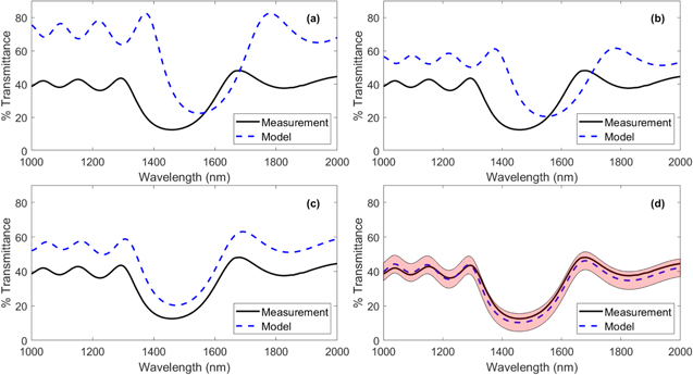
Figure 2. Comparison of simulated versus measured transmission over the course of the characterisation procedure. In each case, (a)–(d), the model is incrementally improved as follows: (a) light emerging from a DBR (into the substrate) with ideal parameters, i.e. grown exactly to design specifications. (b) The effect of including air as the exit medium and allowing multiple incoherent substrate reflections. (c) Individual layer thicknesses measured using BEXP+AFM taken into account. (d) The final result incorporating (b) and (c), plus the measured extinction coefficient of the n-GaAs substrate. The shaded area is the cumulative model error in each of the characterisation methods combined.
Download figure:
Standard image High-resolution image3.2. Finite substrate thickness
The simulation shown in figure 2(a) makes the assumption that incident light terminates inside the substrate and thus treats the substrate as infinite. The simulated 'transmission' in this case is the light that reaches the substrate. This assumption is often the case for optical materials as the substrate is thick enough to absorb the beam and allows for straightforward calculation of reflectance. As a transmission signal is being measured in this work, this assumption is clearly erroneous. Additionally, when allowing for light to emerge from the rear of the sample, one must also account for internal reflection from the sample-air interface at the back of the wafer. This is likely to affect the amplitude of the transmitted light rather than the overall shape of the spectra, as the substrate is thick enough to exclude coherence in multiple reflections.
Including air as an exit medium in the simulation gives the spectrum seen in figure 2(b). As expected, this reduces the inaccuracy in the transmission amplitude, but has little to no effect on the observed shift in wavelength, which indicates a difference between the intended and actual layer thicknesses.
3.3. Determining layer thicknesses
To assess the extent to which the layer thicknesses vary from the design, beam-exit cross-sectional polishing (BEXP), a variant Ar-ion-beam milling technique, was used to prepare a broadened cross-section that can be imaged using atomic force microscopy (AFM). Using this method, it is possible to measure the thickness of thin layers to a high degree of accuracy [10].
The system used was a Leica EM-TIC020 ion beam cutter. Milling was undertaken for 4 h at 7 kV, followed by a 1 kV step for 5 min to polish the surface. The sample was then cleaned with acetone and isopropyl alcohol (IPA) in an ultrasonic bath for ten minutes each. To ensure sample contrast using contact mode AFM, the sample was etched using a 4:1 citric acid (saturated):hydrogen peroxide (27%) mixture for 5 s, etch stopped with deionized water and cleaned in IPA for a subsequent 5 min in an ultrasonic bath. Layer measurements were taken using a Bruker MultiMode 8 AFM, with BudgetSensors Multi75Al-G probes in contact mode.
Figure 3 shows the cross-section obtained using BEXP and AFM. The thicknesses calculated from this measurement are given in table 1. Both the GaAs and Al0.9Ga0.1As layers have been grown thinner than intended, with the average GaAs thickness at 110 ± 2 nm (compared to the target of 115.0 nm) and the average Al0.9Ga0.1As thickness at 123 ± 2 nm (compared to the target of 130.7 nm). Other methods could also be used, such as transmission electron microscopy (TEM). It should be noted that the sample used here was grown in an unconditioned MBE chamber and had little in the way of calibration, so variation from specification is expected.
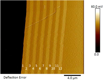
Figure 3. AFM image of the structure cross-sectioned using BEXP. Paler layers are AlxGa1−xAs and darker layers are GaAs.
Download figure:
Standard image High-resolution imageTable 1. Cross-sectional measurements of the DBR sample showing the target thicknesses, the measured thicknesses, and the differences between them. The layer numbers in column 1 correspond to those in figure 3.
| Target | BEXP | |||
|---|---|---|---|---|
| Layer | thickness | thickness | Difference | |
| No. | Material | (nm) | (nm) | (nm) |
| 1 | GaAs | 115 | 108 ± 4 | −7 |
| 2 | Al0.9Ga0.1As | 131 | 122 ± 5 | −9 |
| 3 | GaAs | 115 | 107 ± 4 | −8 |
| 4 | Al0.9Ga0.1As | 131 | 122 ± 5 | −9 |
| 5 | GaAs | 115 | 110 ± 4 | −5 |
| 6 | Al0.9Ga0.1As | 131 | 125 ± 5 | −6 |
| 7 | GaAs | 115 | 112 ± 4 | −3 |
| 8 | Al0.9Ga0.1As | 131 | 121 ± 5 | −10 |
| 9 | GaAs | 115 | 112 ± 4 | −3 |
| 10 | Al0.9Ga0.1As | 131 | 123 ± 5 | −8 |
| 11 | GaAs | 115 | 113 ± 4 | −2 |
| 12 | Al0.9Ga0.1As | 131 | 128 ± 5 | −3 |
| Substr. | GaAs | — | — | — |
Including the individual layer thicknesses in the simulation gives the spectrum shown in figure 2(c). The shift in wavelength has been almost fully corrected, and there is only a small (10%–15%) amplitude shift in the transmission. Such a uniform shift cannot be due to individual variations in the layers as this would have an effect on the shape of the spectrum as well as the amplitude. It is reasonable to infer that the shift is due to some characteristic of the substrate that has yet to be taken into account.
3.4. Substrate calibration
Another assumption of the system being modelled is that the n-GaAs substrate is completely transparent in our region of interest (1–2 μm). If the wafer was undoped then this assumption would be correct. However, the silicon doping of this batch of wafers has a specified carrier concentration of (1.21–3.69) × 1018 cm−3, and has the potential to absorb a significant amount of light in the substrate. The grown layers are undoped in this case to avoid the extra variation between layers. Assuming that the real components of the refractive indices of the materials are not affected far from the band-gap edge, it is possible to discern the absorption of an unused n-GaAs wafer from the same batch using the relation

where R is the reflectance, T is the transmittance, and A is the absorptance of the wafer. The reflectance is measured using the Cary 5000 spectrophotometer with an integrating sphere attachment, and the transmittance is measured using the standard transmission mode. The resulting absorptance is calculated using (1) and is shown in figure 4.
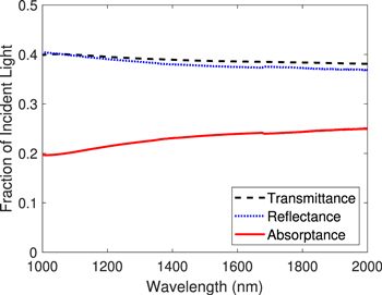
Figure 4. The transmittance, reflectance, and calculated absorptance of the Si doped n-GaAs substrate. The batch of wafers that the substrate is from are stated to be 361 ± 9 μm thick with a carrier concentration of (1.21–3.69) × 1018 cm−3.
Download figure:
Standard image High-resolution imageUsing the data shown in figure 4 it is possible to numerically calculate the extinction coefficient ks. Refractive index data is used to determine the reflection RI from the semiconductor-air and air-semiconductor interfaces with the expression

where ns and na are the refractive indices of the semiconductor and air respectively. The intensity It of propagating light with wavelength λ after travelling through a wafer with thickness t is given as

where ks is the extinction coefficient of the material and I is the incident light intensity. Both (2) and (3) use the assumption that the real part of the refractive index does not vary significantly with doping far from the band gap edge.
Figure 5 shows the simulated optical path used in calculating the total reflectivity of the GaAs wafer to compare to the measurement in figure 4. Reflection and transmission at each boundary is calculated using (2), and the downwards and upwards propagation losses are calculated using (3). The total reflectivity RT is given as

where the number of internal reflections, N, is high enough that the contribution RN to the total reflectivity becomes negligible. This process is repeated with incrementally increasing values of ks until the magnitude of the reflection is in agreement with the measured data, and is replicated for each wavelength. Figure 6 shows the result of the ks calculation for the n-doped GaAs wafer.
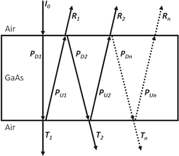
Figure 5. Components of the simulated light path incident on the GaAs wafer. I0 is the incident intensity, Ri are the components of the total reflection, Ti are the components of the total transmission and PD(i) and PU(i) are the downwards and upwards propagating components respectively. The angled paths are for clarity, all components are normal to the sample surface.
Download figure:
Standard image High-resolution image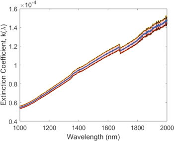
Figure 6. Calculated extinction coefficient of the Si doped GaAs wafer used as a substrate. The shaded area denotes the error in ks due to the uncertainty in the thickness of the wafer.
Download figure:
Standard image High-resolution imageWhile the values of ks in figure 6 are small (of the order of 10−4) they have a measurable effect on the overall optical properties of the wafer. The step between 1360 nm and 1680 nm is a known detector artefact that has been viewed on multiple different samples and is currently under investigation. Incorporating this absorption into the DBR transmittance simulation gives the spectrum shown in figure 2(d). This adjustment to the simulation means that the model is in good agreement with the measurement. The shaded area is the cumulative error in the various parameters used to improve the calculation, such as uncertainty in epitaxial layer thickness and the extinction coefficient. Since the measurement is well within the error region it would be difficult to improve this further. However, one characteristic that has yet to be analysed is the alloy composition of the AlxGa1−xAs layers. Since the refractive index of these layers is dependent on the ratio of aluminium to gallium, it is logical to check that composition matches the intended specifications (Al0.9Ga0.1As).
3.5. Determining AlxGa1−xAs composition
There are several available methods to assess the composition of an AlxGa1−xAs crystal such as high-resolution x-ray diffraction (HRXRD) [11–14], TEM [11], photoluminescence (PL) [11, 12, 14], Raman spectroscopy [12, 13], secondary ion mass spectroscopy (SIMS) [15, 16], and x-ray photoelectron spectroscopy [17]. The main limitation with HRXRD, PL and Raman is that they work well on bulk samples, or with single layers on or near the surface, but cannot analyse many-layered structures; especially if the structure has multiple layers with similar compositions. Most also require complex fitting analyses, and there are often discrepancies between techniques [14]. Devices that use DBRs are usually relatively thick, with many thinner layers. For example, a typical VCSEL can have ∼100 layers, each of the order of 100 nm, making compositional analysis of individual layers with these techniques very difficult or even impossible.
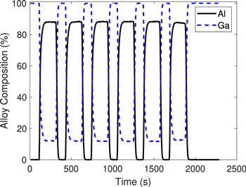
Magnetic-sector SIMS depth profiling was carried out using a CAMECA IMS 4f secondary-ion mass spectrometer. The analysis conditions used a Cs+ primary ion beam with an impact energy of 5.5 keV and beam current of 30 nA. The beam was rastered across the sample surface with an area of 125 μm × 125 μm and positive secondary ions collected from an analysis area of approximately 80 μm2. The CsAl+, CsGa+ and CsAs+ polyatomic species were detected as these are reported to be relatively free of SIMS matrix effects and the relative levels of gallium and aluminium were then calculated using a correlation plot of the CsAl+/CsAs+ and CsGa+/CsAs+ signals [18].
The depth profile in figure 7 shows that the sample has good uniformity throughout its 12 layers. Table 2 lists the measured composition for each layer of the sample. The average Al content is 88.0% ± 0.3%, which is lower than intended, but still within a reasonable margin of the specification. A simulation was performed using these values but the difference to the result in figure 2(d) is marginal. By varying the Al content in the simulation it was found that the content could be reduced by ∼10% before a significant portion of the data is outside the error bars of the simulation implying the design is tolerant to small variations in composition.
Figure 7. Depth profile performed using magnetic-sector SIMS with the top layer on the left and the substrate on the right. Alloy composition is calculated from Al and Ga only, i.e. Al0.9Ga0.1As corresponds to 90% aluminium and 10% gallium.
Download figure:
Standard image High-resolution image
Table 2. Average compositional data from each layer of the structure.
| Layer No. | Aluminium (%) | Gallium (%) |
|---|---|---|
| 1 | 0.00 | 100.00 |
| 2 | 87.94 | 12.06 |
| 3 | 0.01 | 99.99 |
| 4 | 88.08 | 11.92 |
| 5 | 0.01 | 99.99 |
| 6 | 88.20 | 11.80 |
| 7 | 0.01 | 99.99 |
| 8 | 88.26 | 11.74 |
| 9 | 0.01 | 99.99 |
| 10 | 88.24 | 11.76 |
| 11 | 0.01 | 99.99 |
| 12 | 87.45 | 12.55 |
| Substrate | — | — |
4. Conclusions
We have studied the material properties of a GaAs/Al0.9Ga0.1As distributed Bragg reflector to improve the consistency between simulated and measured optical properties. Internal reflections from the backside of the wafer were included in the simulation to account for the sample-air interface. Layer thicknesses measured using BEXP and AFM were found to be thinner than expected, with an average variation of 6 ± 3 nm from the target thickness. The extinction coefficient of a nominally identical substrate was measured using combined reflectance and transmittance data from 1 to 2 μm, and included in the simulation. The composition of the AlxGa1−xAs layers was measured using SIMS and were found to be lower than the target value, with an average value of 88.0% ± 0.3%.
From figure 3 it can be ascertained that the layer interfaces are of a high quality, as such the roughness was not included in the simulation. Any irregularity present in the interface will produce a distribution in the thicknesses, thus broadening the measurement. While doping was not included in the epitaxial layers, a doped DBR with many layers has the potential to absorb, and as such the data from the calibration in this work could potentially be used in further layer modelling, if the dopant type and carrier concentration were consistent between calibration and growth.
We have found that accurate layer thicknesses are critical to simulating the features of the sample correctly. Substrate corrections (internal reflections and absorption) only affected the transmission amplitude and not the overall shape of the spectrum but are still important for matching the data with the model. While the Al content of the AlxGa1−xAs was slightly lower than expected, the effect on the transmission was minimal, implying a reasonable tolerance to composition.
Acknowledgments
This work was partly supported by a CASE award EP/N509504/1 from the Engineering and Physical Sciences Research Council, UK, by IQE plc and Innovate UK project no. 103 444. We would also like to thank Dr Lefteris Danos for kindly allowing us the use of his equipment.
Data availability
The datasets used in generating the figures are available at https://doi.org/10.17635/lancaster/researchdata/343.